

Page 1

INTEGRATED CIRCUITS
TDF5140A
Brushless DC motor drive circuit
Product specification 1999 March 15
Page 2

Philips Semiconductors Product specification
Brushless DC motor drive circuit TDF5140A
FEATURES
• Full-wave commutation (using push/pull drivers at the
output stages) without position sensors
• Built-in start-up circuitry
• Three push-pull outputs:
– 0.8 A output current (typ.)
APPLICATIONS
• VCR
• Laser beam printer
• Fax machine
• Blower
• Automotive.
– low saturation voltage
– built-in current limiter
• Thermal protection
• Flyback diodes
• Tacho output without extra sensor
• Position pulse stage for phase-locked-loop control
GENERAL DESCRIPTION
The TDF5140A is a bipolar integrated circuit used to drive
3-phase brushless DC motors in full-wave mode. The
device is sensorless (saving of 3 hall-sensors) using the
back-EMF sensing technique to sense the rotor position.
• Transconductance amplifier for an external control
transistor.
QUICK REFERENCE DATA Measured over full voltage and temperature range.
SYMBOL PARAMETER CONDITIONS MIN. TYP. MAX. UNIT
V
V
P
VMOT
supply voltage note 1 4 − 18 V
input voltage to the output
note 2 1.7 − 20 V
driver stages
V
I
DO
LIM
drop-out output voltage IO = 100 mA − 0.93 1.05 V
current limiting V
= 10 V; RO= 3.9 Ω 0.7 0.8 1 A
VMOT
Notes
1. An unstabilized supply can be used.
2. V
= VP; +AMP IN = −AMP IN = 0 V; all outputs IO = 0 mA.
VMOT
ORDERING INFORMATION
PACKAGE
EXTENDED TYPE NUMBER
PINS PIN POSITION MATERIAL CODE
TDF5140A 18 DIL plastic SOT102
1999 March 15 2
Page 3
Philips Semiconductors Product specification
Brushless DC motor drive circuit TDF5140A
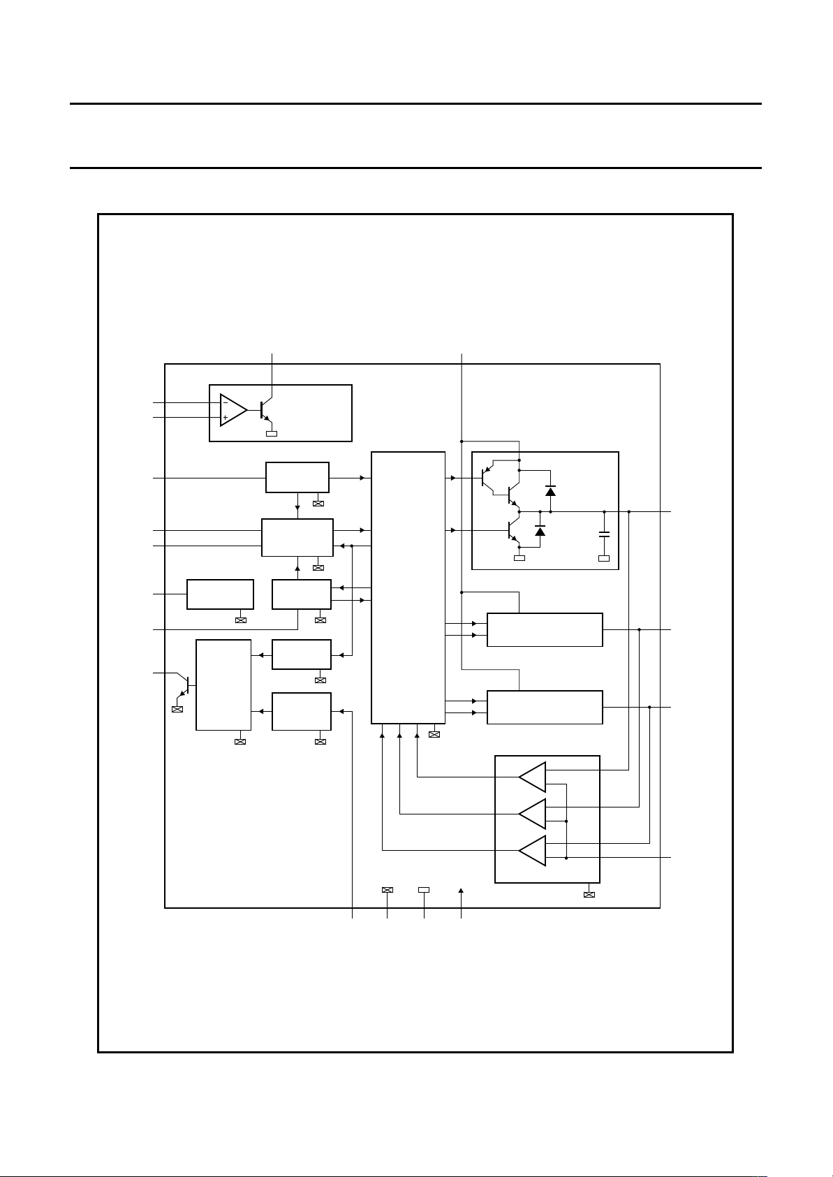
BLOCK DIAGRAM
−AMP IN
+AMP IN
CAP-ST
CAP-DC
CAP-CD
TEST
CAP-TI
PG/FG
13
14
11
10
9
2
PROTECTION
12
6
THERMAL
ROTATION
POSITION
SPEED
&
DETECTOR
OUTPUT
STAGE
AMP OUT
15
CONDUCTANCE
AMPLIFIER
START-UP
OSCILLATOR
ADAPTIVE
COMMUTATION
DELAY
TIMING
DIVIDE
POSITION
DETECTOR
STAGE
TRANS-
BY 2
COMMUTATION
LOGIC
VMOT
4
PUSH/PULL
FLYBACK
D
H
OUTPUT
D
L
DRIVER
STAGE 1
OUTPUT DRIVER
STAGE 2
OUTPUT DRIVER
STAGE 3
1
MOT1
3
MOT2
16
MOT3
TDF5140A
57 8
PGIN GND218GND1 V
Fig.1 Block diagram
1999 March 15 3
P
EMF COMPARATORS
17
MGH313
MOT0
Page 4

Philips Semiconductors Product specification
Brushless DC motor drive circuit TDF5140A
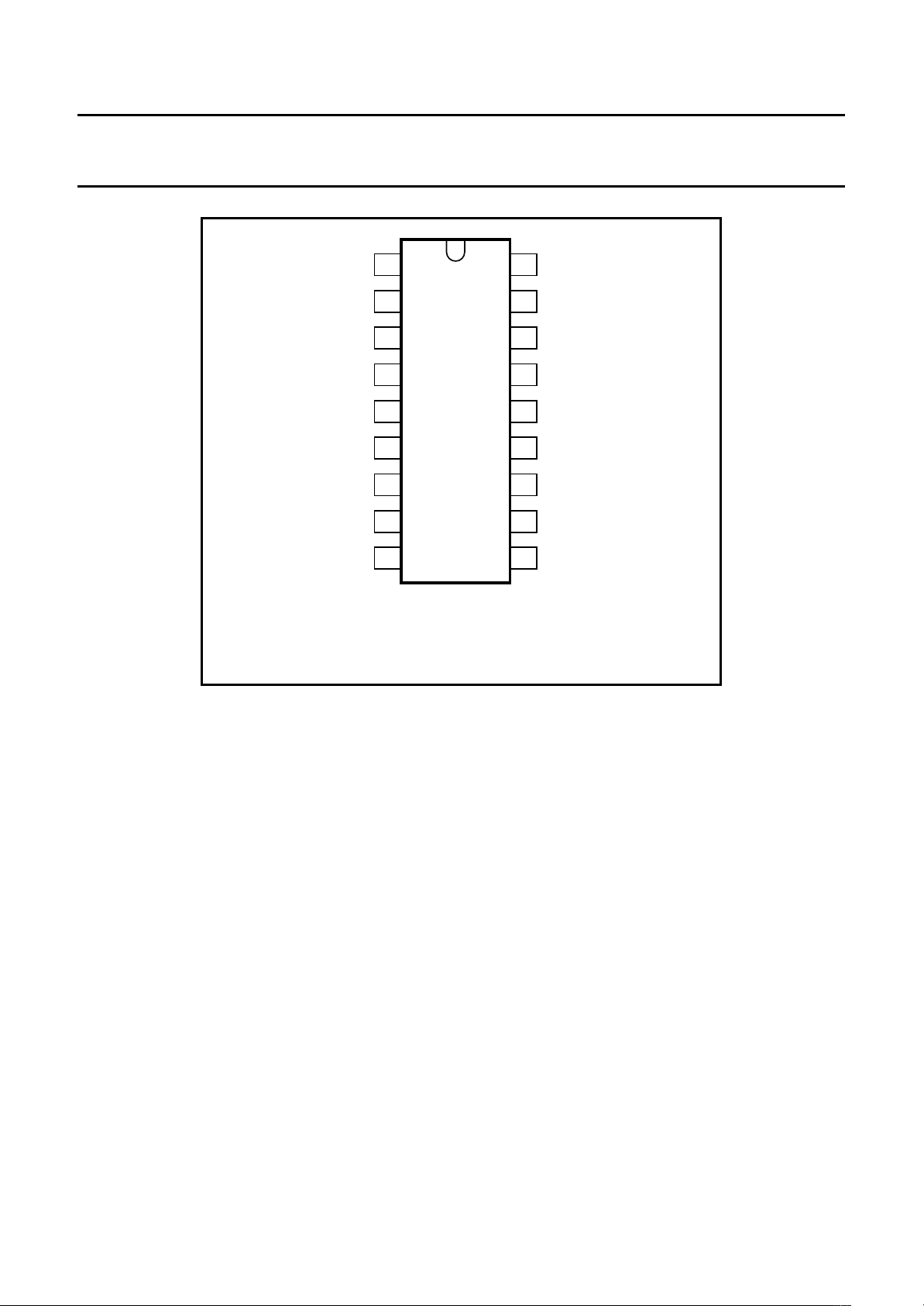
PINNING
SYMBOL
MOT1 1 driver output 1
TEST 2 test input/output
MOT2 3 driver output 2
VMOT 4 input voltage for the output driver stages
PG IN 5 position generator: input from the position detector sensor to the position
PG/FG 6 position generator/frequency generator: output of the rotation speed and position
GND2 7 ground supply return for control circuits
V
P
CAP-CD 9 external capacitor connection for adaptive communication delay timing
CAP-DC 10 external capacitor connection for adaptive communication delay timing copy
CAP-ST 11 external capacitor connection for start-up oscillator
CAP-TI 12 external capacitor connection for timing
+AMP IN 13 non-inverting input of the transconductance amplifier
−AMP IN 14 inverting input of the transconductance amplifier
AMP OUT 15 transconductance amplifier output (open collector)
MOT3 16 driver output 3
MOT0 17 input from the star point of the motor coils
GND1 18 ground (0 V) motor supply return for output stages
PIN
DIL18
detector stage (optional); only if an external position coil is used
detector stages (open collector digital output, negative-going edge is valid)
8 positive supply voltage
DESCRIPTION
1999 March 15 4
Page 5
Philips Semiconductors Product specification
Brushless DC motor drive circuit TDF5140A
MOT1
TEST
MOT2
VMOT
PG IN
PG/FG
GND2
Vp
CAP-CD
1
2
3
4
5
TDF5140A
6
7
8
9
MGH311
Fig.2 Pin configuration
18
17
16
15
14
13
12
11
10
+AMP IN
CAP-TI
GND1
MOT0
MOT3
AMP OUT
-AMP IN
CAP-ST
CAP-DC
FUNCTIONAL DESCRIPTION
The TDF5140A offers a sensorless three phase motor drive function. It is unique in its combination of sensorless motor
drive and full-wave drive. The TDF5140A offers protected outputs capable of handling high currents and can be used
with star or delta connected motors. It can easily be adapted for different motors and applications. The TDF5140A offers
the following features:
• Sensorless commutation by using the motor EMF.
• Built-in start-up circuit.
• Optimum commutation, independent of motor type or motor loading.
• Built-in flyback diodes.
• Three phase full-wave drive.
• High output current (0.8 A).
• Outputs protected by current limiting and thermal protection of each output transistor.
• Low current consumption by adaptive base-drive.
• Accurate frequency generator (FG) by using the motor EMF.
• Amplifier for external position generator (PG) signal.
• Suitable for use with a wide tolerance, external PG sensor.
• Built-in multiplexer that combines the internal FG and external PG signals on one pin for easy use with a controlling
microprocessor.
• Uncommitted operational transconductance amplifier (OTA), with a high output current, for use as a control amplifier.
1999 March 15 5
Page 6
Philips Semiconductors Product specification
Brushless DC motor drive circuit TDF5140A
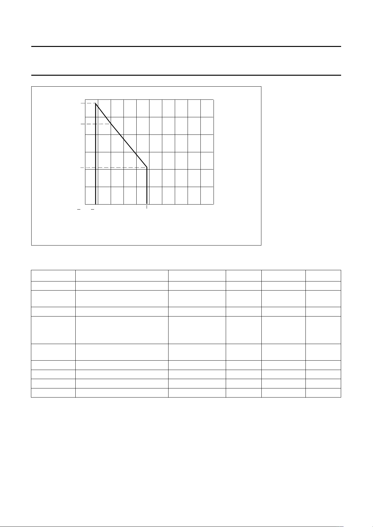
amb
MBD535
o
2.80
P
(W)
tot
2.28
1.05
3
2
0
50
0 200
30
50 100 150
70
T ( C)
Fig.3 Power derating curve (SOT102; DIL18).
LIMITING VALUES
In accordance with the Absolute Maximum Rating System (IEC 134).
SYMBOL PARAMETER CONDITIONS MIN. MAX. UNIT
V
P
V
I
supply voltage − 18 V
input voltage; all pins except
VI< 18 V −0.3 VP + 0.5 V
VMOT
V
V
V
VMOT
O
I
VMOT input voltage −0.5 20 V
output voltage
AMP OUT and PG/FG GND V
MOT1, MOT2 and MOT3 −1V
input voltage CAP-ST, CAP-TI,
− 2.5 V
P
VMOT
+ V
DHF
CAP-CD and CAP-DC
T
stg
T
amb
P
tot
V
es
storage temperature −55 +150 °C
operating ambient temperature −30 +70 °C
total power dissipation see Fig. 3 −− W
electrostatic handling see “Handling” − 500 V
V
V
HANDLING
Every pin withstands the ESD test in accordance with
“MIL-STD-883C class 2”
3 pulses + and 3 pulses − on each pin referenced to ground.
1999 March 15 6
. Method 3015 (HBM 1500 Ω, 100 pF)
Page 7

Philips Semiconductors Product specification
Brushless DC motor drive circuit TDF5140A
CHARACTERISTICS
= 14.5 V; T
V
P
=25°C; unless otherwise specified.
amb
SYMBOL PARAMETER CONDITIONS MIN. TYP. MAX. UNIT
Supply
V
I
P
V
P
VMOT
supply voltage note 1 4 − 18 V
supply current note 2 − 3.7 5 mA
input voltage to the output driver
see Fig.1 1.7 − 20 V
stages
Thermal protection
T
SD
local temperature at
130 140 150 °C
temperature sensor causing
shut-down
∆T reduction in temperature before
after shut-down − T
− 30 − K
SD
switch-on
MOT0; centre tap
V
I
I
V
∆V
I
CSW
CSW
input voltage −0.5 − V
input bias current 0.5 V < VI< V
− 1.5 V −10 − 0 µA
VMOT
VMOT
comparator switching level note 3 ±20 ±30 ±40 mV
variation in comparator
−3 0 +3 mV
switching levels
V
hys
comparator input hysteresis − 75 −µV
MOT1, MOT2 and MOT3
V
∆V
DO
OL
drop-out output voltage IO = 100 mA − 0.93 1.05 V
= 500 mA − 1.65 1.80 V
I
O
variation in saturation voltage
IO = 100 mA −− 180 mV
between lower transistors
∆V
OH
variation in saturation voltage
IO = −100 mA −− 180 mV
between upper transistors
I
V
LIM
DHF
current limiting V
diode forward voltage (diode DH)IO = −500 mA; notes 4
= 10 V; RO= 6.8 Ω 0.7 0.8 1 A
VMOT
−− 1.5 V
and 5; see Fig.1
V
DLF
diode forward voltage (diode DL)IO = 500 mA; notes 4 and
−1.5 −−V
5; see Fig.1
I
DM
peak diode current note 5 −− 1A
+AMP IN and −AMP IN
V
I
input voltage −0.3 − VP− 1.7 V
differential mode voltage without
−− ±V
P
'latch-up'
I
b
C
I
V
offset
input bias current −− 650 nA
input capacitance − 4 − pF
input offset voltage −− 10 mV
V
V
1999 March 15 7
Page 8

Philips Semiconductors Product specification
Brushless DC motor drive circuit TDF5140A
SYMBOL PARAMETER CONDITIONS MIN. TYP. MAX. UNIT
AMP OUT (open collector)
I
I
V
sat
V
O
SR slew rate R
G
tr
PG IN
V
I
I
b
R
I
V
CWS
V
hys
PG/FG (open collector)
V
OL
V
OH(max)
t
THL
δ duty factor − 50 − %
t
PL
CAP-ST
I
sink
I
source
V
SWL
V
SWH
CAP-TI
I
sink
I
source
V
SWL
V
SWM
V
SWH
output sink current 40 −−mA
saturation voltage II = 40 mA − 1.5 2.1 V
output voltage −0.5 − +18 V
= 330 Ω; CL = 50 pF − 60 − mA/µs
L
transfer gain 0.3 −−S
input voltage −0.3 − +5 V
input bias current −− 650 nA
input resistance 5 − 30 kΩ
comparator switching level 86 − 107 mV
comparator input hysteresis −±8− mV
LOW level output voltage IO = 1.6 mA −− 0.4 V
maximum HIGH level output
V
P
−−V
voltage
HIGH-to-LOW transition time CL = 50 pF; RL = 10 kΩ− 0.5 −µs
ratio of PG/FG frequency and
− 1 : 2 −
commutation frequency
pulse width LOW after a PG IN pulse 5 7 18 µs
output sink current 1.5 2.0 2.5 µA
output source current −2.5 −2.0 −1.5 µA
LOW level switching voltage − 0.20 − V
HIGH level switching voltage − 2.20 − V
output sink current − 28 −µA
output source current 0.05 V < V
0.3 V < V
CAP-TI
< 0.3 V −−57 −µA
CAP-TI
< 2.2 V −−5−µA
LOW level switching voltage − 50 − mV
MIDDLE level switching voltage − 0.30 − V
HIGH level switching voltage − 2.20 − V
1999 March 15 8
Page 9

Philips Semiconductors Product specification
Brushless DC motor drive circuit TDF5140A
SYMBOL PARAMETER CONDITIONS MIN. TYP. MAX. UNIT
CAP-CD
I
sink
I
source
I
sink/Isource
V
IL
V
IH
CAP-DC
I
sink
I
source
I
sink/Isource
V
IL
V
IH
Notes
1. An unstabilized supply can be used.
2. V
VMOT
3. Switching levels with respect to MOT1, MOT2 and MOT3.
4. Drivers are in the high-impedance OFF-state.
5. The outputs are short-circuit protected by limiting the current and the IC temperature.
output sink current 10.6 16.2 22 µA
output source current −5.3 −8.1 −11 µA
ratio of sink to source current 1.85 2.05 2.25
LOW level input voltage 850 875 900 mV
HIGH level input voltage 2.3 2.4 2.55 V
output sink current 10.1 15.5 20.9 µA
output source current −20.9 −15.5 −10.1 µA
ratio of sink to source current 0.9 1.025 1.15
LOW level input voltage 850 875 900 mV
HIGH level input voltage 2.3 2.4 2.55 V
= VP, all other inputs at 0 V; all outputs at VP; IO = 0 mA.
APPLICATION INFORMATION
full pagewidth
GND1
(1) Value selected for 3 Hz
start-up oscillator frequency
(1) Value selected for 3 Hz start-up oscillator frequency.
Fig.4 Application diagram without use of the operational transconductance amplifier (OTA).
(1)
220
10
nF
nF
18 17 16 15 14 13 12 1011
TDF5140A
1234567 98
PGIN
VMOT
10 µF
PG/FG
18 nF
18 nF
V
P
MBK985
1999 March 15 9
Page 10

Philips Semiconductors Product specification
Brushless DC motor drive circuit TDF5140A
Introduction (see Fig.5)
Full-wave driving of a three phase motor requires three
push-pull output stages. In each of the six possible states
two outputs are active, one sourcing (H) and one sinking
(L). The third output presents a high impedance (Z) to the
motor which enables measurement of the motor
back-EMF in the corresponding motor coil by the EMF
comparator at each output. The commutation logic is
responsible for control of the output transistors and
selection of the correct EMF comparator. In Table 1 the
sequence of the six possible states of the outputs has
been depicted.
Table 1 Output states.
STATE MOT1
(1)
MOT2
(1)
MOT3
(1)
1ZLH
2HLZ
3HZL
4ZHL
5LHZ
6LZH
Note
1. H = HIGH state;
L = LOW state;
Z = high impedance OFF-state.
Because of high inductive loading the output stages
contain flyback diodes. The output stages are also
protected by a current limiting circuit and by thermal
protection of the six output transistors.
The detected zero-crossings are used to provide speed
information. The information has been made available on
the PG/FG output pin. This is an open collector output and
provides an output signal with a frequency that is half the
commutation frequency. A VCR scanner also requires a
PG phase sensor. This circuit has an interface for a simple
pick-up coil. A multiplexer circuit is also provided to
combine the FG and PG signals in time.
The system will only function when the EMF voltage from
the motor is present. Therefore, a start oscillator is
provided that will generate commutation pulses when no
zero-crossings in the motor voltage are available.
A timing function is incorporated into the device for internal
timing and for timing of the reverse rotation detection.
The TDF5140A also contains an uncommitted
transconductance amplifier (OTA) that can be used as a
control amplifier. The output is capable of directly driving
an external power transistor.
The TDF5140A is designed for systems with low current
consumption: use of I2L logic, adaptive base drive for the
output transistors (patented), possibility of using a pick-up
coil without bias current.
The zero-crossing in the motor EMF (detected by the
comparator selected by the commutation logic) is used to
calculate the correct moment for the next commutation,
that is, the change to the next output state. The delay is
calculated (depending on the motor loading) by the
adaptive commutation delay block.
1999 March 15 10
Page 11

Philips Semiconductors Product specification
Brushless DC motor drive circuit TDF5140A
handbook, full pagewidth
47 kΩ
from
DAC
220 nF
18 nF
18 nF
TEST
10 nF
FG to
micro-
processor
+5 V
4.7
39 kΩ
BY 2
10 kΩ
47 nF
13
1 µF
COMMUTATION
LOGIC
TP
D
TN
D
TN
TP
D
TN
D
TN
TP
D
TN
D
TN
1
3
16
SCANNER
MOTOR
POSITION
COIL
BD434
+14 V
14
11
10
9
2
12
6
kΩ
680 Ω
47 nF
THERMAL
PROTECTION
ROTATION
SPEED/
DETECTOR
OUTPUT
STAGE
470 Ω
120 Ω
15 4 18
START-UP
OSCILLATOR
ADAPTIVE
COMMUTATION
DELAY
TIMING
DIVIDE
POSITION
DETECTOR
STAGE
8
V
P
GND2
GND1
TDF5140A
75
Fig.5 Typical application of the TDF5140A as a scanner driver, with use of OTA.
1999 March 15 11
17
EMF COMPARATORS
MBK986
Page 12

Philips Semiconductors Product specification
Brushless DC motor drive circuit TDF5140A
Adjustments
The system has been designed in such a way that the
tolerances of the application components are not critical.
However, the approximate values of the following
components must still be determined:
• The start capacitor; this determines the frequency of the
start oscillator.
• The two capacitors in the adaptive commutation delay
circuit; these are important in determining the optimum
moment for commutation, depending on the type and
loading of the motor.
• The timing capacitor; this provides the system with its
timing signals.
HE START CAPACITOR (CAP-ST)
T
This capacitor determines the frequency of the start
oscillator. It is charged and discharged, with a current of
2 µA, from 0.05 to 2.2 V and back to 0.05 V. The time
taken to complete one cycle is given by:
t
= (2.15 × C) s (with C in µF)
start
The start oscillator is reset by a commutation pulse and so
is only active when the system is in the start-up mode. A
pulse from the start oscillator will cause the outputs to
change to the next state (torque in the motor). If the
movement of the motor generates enough EMF the
TDF5140A will run the motor. If the amount of EMF
generated is insufficient, then the motor will move one step
only and will oscillate in its new position. The amplitude of
the oscillation must decrease sufficiently before the arrival
of the next start pulse, to prevent the pulse arriving during
the wrong phase of the oscillation. The oscillation of the
motor is given by:
f
osc
=
1
---------------------------------- K
I× p×
t
2π
---------------------- -
J
where:
= torque constant (N.m/A)
K
t
I = current (A)
p = number of magnetic pole-pairs
J = inertia J (kg.m2)
Example: J = 72 × 10-6kg.m2, K = 25 × 10-3N.m/A, p = 6
and I = 0.5 A; this gives f
= 5 Hz. If the damping is high
osc
then a start frequency of 2 Hz can be chosen or t = 500 ms,
thus C = 0.5/2 = 0.25 µF, (choose 220 nF).
HE ADAPTIVE COMMUTATION DELAY (CAP-CD AND
T
CAP-DC)
In this circuit capacitor CAP-CD is charged during one
commutation period, with an interruption of the charging
current during the diode pulse. During the next
commutation period this capacitor (CAP-CD) is discharged
at twice the charging current. The charging current is
8.1 µA and the discharging current 16.2 µA; the voltage
range is from 0.9 to 2.2 V. The voltage must stay within this
range at the lowest commutation frequency of interest, f
6–
×
8.1 10
==
C
-------------------------f1.3×
6231
------------ f
c1
(C in nF)
C1
If the frequency is lower, then a constant commutation
delay after the zero-crossing is generated by the discharge
from 2.2 to 0.9 V at 16.2 µA.
maximum delay = (0.076 × C) ms (with C in nF)
Example: nominal commutation frequency = 900 Hz and
the lowest usable frequency = 400 Hz, so:
CAP-CD
6231
------------ 400
15.6==
(choose 18 nF)
The other capacitor, CAP-DC, is used to repeat the same
delay by charging and discharging with 15.5 µA. The same
value can be chosen as for CAP-CD. Fig.6 illustrates
typical voltage waveforms.
:
1999 March 15 12
Page 13

Philips Semiconductors Product specification
Brushless DC motor drive circuit TDF5140A
handbook, full pagewidth
voltage
on CAP-CD
voltage
on CAP-DC
Fig.6 CAP-CD and CAP-DC typical voltage waveforms in normal running mode.
THE TIMING CAPACITOR (CAP-TI)
Capacitor CAP-TI is used for timing the successive steps
within one commutation period; these steps include some
internal delays.
The most important function is the watchdog time in which
the motor EMF has to recover from a negative diode-pulse
back to a positive EMF voltage (or vice versa). A watchdog
timer is a guarding function that only becomes active when
the expected event does not occur within a predetermined
time.
The EMF usually recovers within a short time if the motor
is running normally (<<ms). However, if the motor is
motionless or rotating in the reverse direction, then the
time can be longer (>>ms).
A watchdog time must be chosen so that it is long enough
for a motor without EMF (still) and eddy currents that may
stretch the voltage in a motor winding; however, it must be
short enough to detect reverse rotation. If the watchdog
t
MGH317
time is made too long, then the motor may run in the wrong
direction (with little torque).
The capacitor is charged, with a current of 57 µA, from
0.2 to 0.3 V. Above this level it is charged, with a current of
5 µA, up to 2.2 V only if the selected motor EMF remains
in the wrong polarity (watchdog function). At the end, or, if
the motor voltage becomes positive, the capacitor is
discharged with a current of 28 µA. The watchdog time is
the time taken to charge the capacitor, with a current of
5 µA, from 0.3 to 2.2 V.
To ensure that the internal delays are covered CAP-TI
must have a minimum value of 2 nF. For the watchdog
function a value for CAP-TI of 10 nF is recommended.
To ensure a good start-up and commutation, care must be
taken that no oscillations occur at the trailing edge of the
flyback pulse. Snubber networks at the outputs should be
critically damped.
Typical voltage waveforms are illustrated by Fig.7.
1999 March 15 13
Page 14

Philips Semiconductors Product specification
Brushless DC motor drive circuit TDF5140A
k, full pagewidth
V
MOT 1
voltage
on CAP-TI
MGH318
If the chosen value of CAP-TI is too small oscillations can occur in certain positions of a blocked rotor. If the chosen value is too large, then it
is possible that the motor may run in the reverse direction (synchronously with little torque).
Fig.7 Typical CAP-TI and V
voltage waveforms in normal running mode.
MOT1
Other design aspects
There are other design aspects concerning the application
of the TDF5140A besides the commutation function. They
are:
• Generation of the tacho signal FG
• A built-in interface for a PG sensor
• General purpose operational transconductance
amplifier (OTA)
• Possibilities of motor control
• Reliability.
SIGNAL
FG
The FG signal is generated in the TDF5140A by using the
zero-crossing of the motor EMF from the three motor
windings. Every zero-crossing in a (star connected) motor
winding is used to toggle the FG output signal. The FG
frequency is therefore half the commutation frequency.
All transitions indicate the detection of a zero-crossing
(except for PG). The negative-going edges are called FG
pulses because they generate an interrupt in a controlling
microprocessor.
The accuracy of the FG output signal (jitter) is very good.
This accuracy depends on the symmetry of the motor's
electromagnetic construction, which also effects the
satisfactory functioning of the motor itself.
Example: A 3-phase motor with 6 magnetic pole-pairs at
1500 rpm and with a full-wave drive has a commutation
frequency of 25 × 6 × 6 = 900 Hz, and generates a tacho
signal of 450 Hz.
PG
SIGNAL
The accuracy of the PG signal in applications such as VCR
must be high (phase information). This accuracy is
obtained by combining the accurate FG signal with the PG
signal by using a wide tolerance external PG sensor. The
external PG signal (PG IN) is only used as an indicator to
select a particular FG pulse. This pulse differs from the
other FG pulses in that it has a short LOW-time of 18 µs
after a HIGH-to-LOW transition. All other FG pulses have
a 50% duty factor (see Fig.8).
For more information also see
EIE/AN 93014”
.
“application note
1999 March 15 14
Page 15

Philips Semiconductors Product specification
Brushless DC motor drive circuit TDF5140A
dbook, full pagewidth
PG IN
MOT3
PG/FG
tolerance on PG IN
Fig.8 Timing and the FG and PG IN signals.
The special PG pulse is derived from the negative-going
zero-crossing from the MOT3 output (pin 16). The external
PG signal (PG IN on pin 5) must sense a positive-going
voltage (>80 mV) within 1.5 to 7.5 commutation periods
before the negative-going zero-crossing in MOT3
(see Fig.8).
The voltage requirements of the PG IN input are such that
an inexpensive pick-up coil can be used as a sensor
(see Fig.9).
Example: If p = 6, then one revolution contains 6 × 6=36
commutations. The tolerance is 6 periods, that is 60
degrees (mechanically) or 6.67 ms at 1500 rpm.
2.2 kΩ
22 nF
MBD696
MGH319
PG IN
GND2
If a PG sensor is not used, the PG IN input must be
grounded, this will result in a 50% duty factor FG signal.
1999 March 15 15
Fig.9 Pick-up coil as PG sensor.
Page 16

Philips Semiconductors Product specification
Brushless DC motor drive circuit TDF5140A
THE OPERATIONAL TRANSCONDUCTANCE AMPLIFIER (OTA)
The OTA is an uncommitted amplifier with a high output
current (40 mA) that can be used as a control amplifier.
The common mode input range includes ground (GND)
and rises to VP− 1.7 V. The high sink current enables the
OTA to drive a power transistor directly in an analog
control amplifier.
Although the gain is not extremely high (0.3 S), care must
be taken with the stability of the circuit if the OTA is used
as a linear amplifier as no frequency compensation has
been provided.
The convention for the inputs (inverting or not) is the same
as for a normal operational amplifier: with a resistor (as
load) connected from the output (AMP OUT) to the positive
supply, a positive-going voltage is found when the
non-inverting input (+AMP IN) is positive with respect to
the inverting input (−AMP IN). Confusion is possible
because a 'plus' input causes less current, and so a
positive voltage.
M
OTOR CONTROL
DC motors can be controlled in an analog manner using
the OTA.
R
ELIABILITY
It is necessary to protect high current circuits and the
output stages are protected in two ways:
• Current limiting of the 'lower' output transistors. The
'upper' output transistors use the same base current as
the conducting 'lower' transistor (+15%). This means
that the current to and from the output stages is limited.
• Thermal protection of the six output transistors is
achieved by each transistor having a thermal sensor
that is active when the transistor is switched on. The
transistors are switched off when the local temperature
becomes too high.
It is possible, that when braking, the motor voltage (via the
flyback diodes and the impedance on VMOT) may cause
higher currents than allowed (>0.6 A). These currents
must be limited externally.
For the control an external transistor is required. The OTA
can supply the base current for this transistor and act as a
control amplifier.
1999 March 15 16
Page 17

Philips Semiconductors Product specification
Brushless DC motor drive circuit TDF5140A
PACKAGE OUTLINES
seating plane
3.9
3.4
0.85
max
22.00
21.35
3.7
4.7
max
max
0.51
min
2.54
(8x)
1.4 max
18
1
0.53
max
10
9
0.254 M
6.48
6.14
0.32 max
8.25
7.80
7.62
9.5
8.3
MSA259
Dimensions in mm.
Fig.10 18-pin dual in-line; plastic (SOT102).
1999 March 15 17
Page 18

Philips Semiconductors Product specification
Brushless DC motor drive circuit TDF5140A
SOLDERING
Plastic dual in-line packages
Y DIP OR WAVE
B
The maximum permissible temperature of the solder is 260 °C; this temperature must not be in contact with the joint for
more than 5 s. The total contact time of successive solder waves must not exceed 5 s.
The device may be mounted up to the seating plane, but the temperature of the plastic body must not exceed the
specified storage maximum. If the printed-circuit board has been pre-heated, forced cooling may be necessary
immediately after soldering to keep the temperature within the permissible limit.
EPAIRING SOLDERED JOINTS
R
Apply the soldering iron below the seating plane (or not more than 2 mm above it). If its temperature is below 300 °C, it
must not be in contact for more than 10 s; if between 300 and 400 °C, for not more than 5 s.
1999 March 15 18
Page 19

Philips Semiconductors Product specification
TDF5140ABrushless DC motor drive circuit
Data sheet status
Product
Data sheet status
Objective
specification
Preliminary
specification
Product
specification
[1] Please consult the most recently issued data sheet before initiating or completing a design.
[2] The product status of the device(s) described in this data sheet may have changed since this data sheet was published. The latest information is available on the Internet at URL
http://www.semiconductors.philips.com.
[1]
status
Development
Qualification
Production
[2]
Definitions
Short-form specification — The data in a short-form specification is extracted from a full data sheet with the same type number and title. For
detailed information see the relevant data sheet or data handbook.
Limiting values definition — Limiting values given are in accordance with the Absolute Maximum Rating System (IEC 60134). Stress above one
or more of the limiting values may cause permanent damage to the device. These are stress ratings only and operation of the device at these or
at any other conditions above those given in the Characteristics sections of the specification is not implied. Exposure to limiting values for extended
periods may affect device reliability.
Application information — Applications that are described herein for any of these products are for illustrative purposes only. Philips
Semiconductors make no representation or warranty that such applications will be suitable for the specified use without further testing or
modification.
Disclaimers
Life support — These products are not designed for use in life support appliances, devices or systems where malfunction of these products can
reasonably be expected to result in personal injury . Philips Semiconductors customers using or selling these products for use in such applications
do so at their own risk and agree to fully indemnify Philips Semiconductors for any damages resulting from such application.
Right to make changes — Philips Semiconductors reserves the right to make changes, without notice, in the products, including circuits, standard
cells, and/or software, described or contained herein in order to improve design and/or performance. Philips Semiconductors assumes no
responsibility or liability for the use of any of these products, conveys no license or title under any patent, copyright, or mask work right to these
products, and makes no representations or warranties that these products are free from patent, copyright, or mask work right infringement, unless
otherwise specified.
Contact information
For additional information please visit
http://www.semiconductors.philips.com . Fax: +31 40 27 24825
For sales offices addresses send e-mail to:
sales.addresses@www.semiconductors.philips.com.
Definitions
This data sheet contains data from the objective specification for product development.
Philips Semiconductors reserves the right to change the specification in any manner without notice.
This data sheet contains data from the preliminary specification. Supplementary data will be
published at a later date. Philips Semiconductors reserves the right to change the specification
without notice, in order to improve the design and supply the best possible product.
This data sheet contains data from the product specification. Philips Semiconductors reserves the
right to make changes at any time in order to improve the design, manufacturing and supply.
Changes will be communicated according to the Customer Product/Process Change Notification
(CPCN) procedure SNW-SQ-650A.
Koninklijke Philips Electronics N.V. 1999
All rights reserved. Printed in U.S.A.
Date of release: 03-99
Document order number: 9397 750 08754
yyyy mmm dd
1
 Loading...