

Page 1
.OUTPUT CURRENT UP TO2.5A
.WIDE RANGE OF SUPPLY VOLTAGE : + 8 V
TO + 26 V
.CAN WITHSTAND OVERVOLTAGES OF AS
HIGHAS 60 VBETWEEN V
ANDGROUND
CC
.OUTPUT VOLTAGECAN SWING TO LOWER
THAN GROUND
.”SENSE” AND”ALARM”OUTPUTSAREOPEN
COLLECTOROUTPUTS
DESCRIPTION
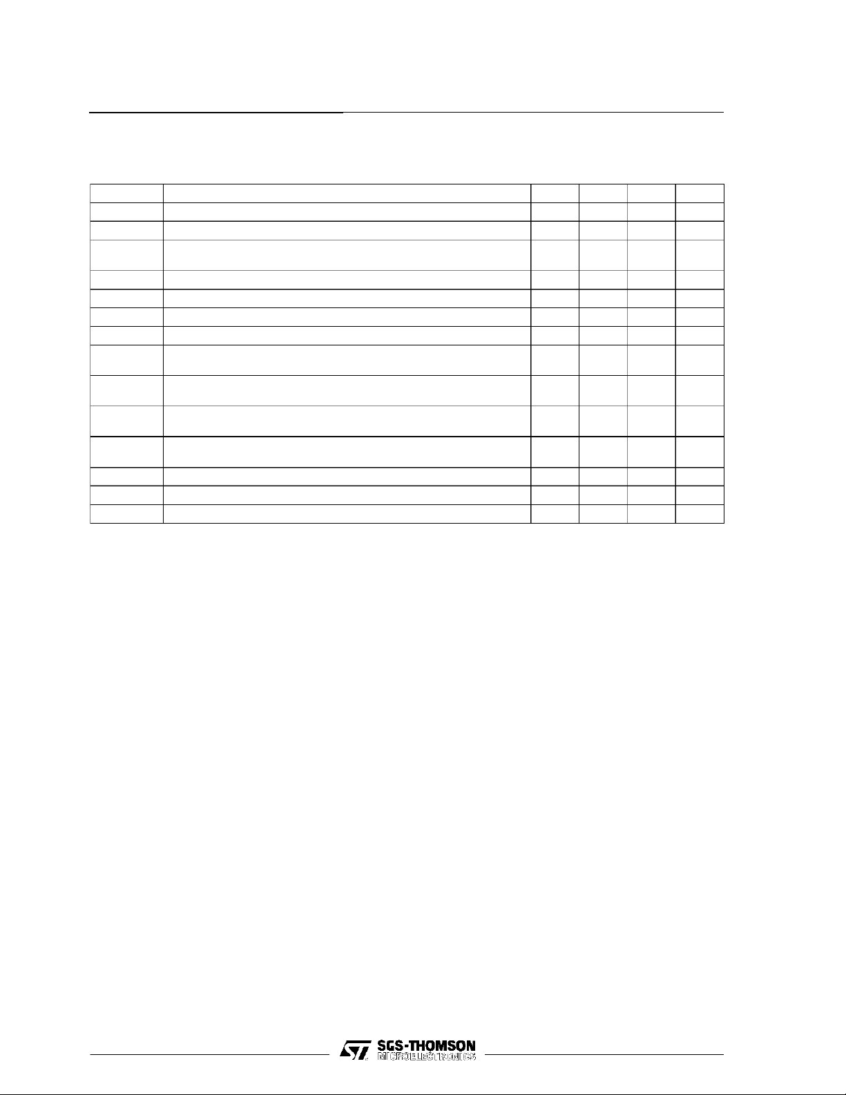
The TDF1779A is a dual source driver delivering
hihgoutputcurrentsandthecapabilitytodrivehighly
inductive loads (Electrovalves, contractors, relays...).
This deviceis essentiallyblow-outproof,each output isprotectedagainstshort-circuits.Ifinternaldissipationbecomestoohigh,driverswillshutdownto
prevent excessive heating. An ”ALARM” output is
providedto indicatetheactionofthethermalprotection.Toreactivatethepoweroutputs,theresetinput
mustbe forcedtolow state.
”SENSE” information of both power outputs are
ORedtogetherand thenprocessedinternally.
A ”STROBE”input isalsoprovidedtoofferthepossibilityof disablingthe power outputs.
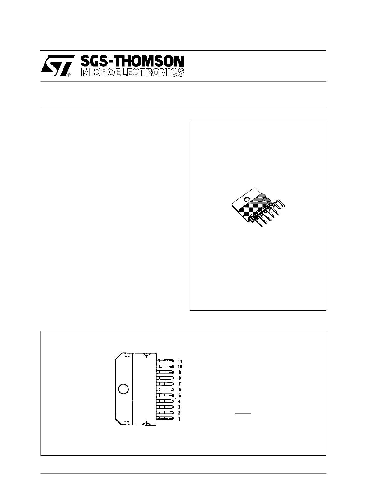
TDF1779A
DUAL 2-A SOURCE DRIVER
MULTIWATT-11
ORDERINGNUMBER : TDE 1779ASP
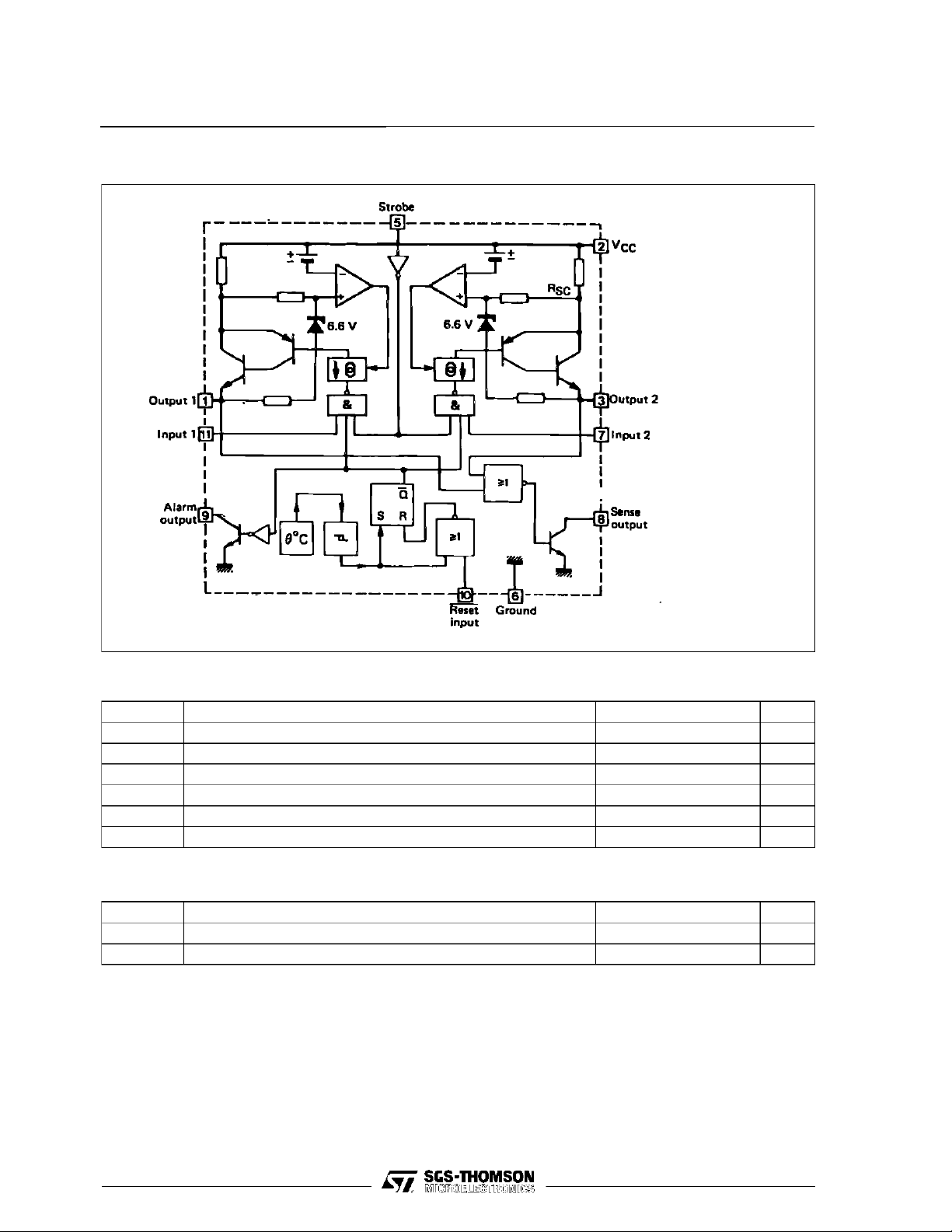
PIN CONNE CTION
April1993
Tab isconnected to pin 6
1 - Output 1
2-V
CC
3 - Output 2
4 - N.C.
5 - Strobe
6 - Ground
7 - Input2
8 - Senseoutput
9 - Alarm output
10 - Resetinput
11 - Input1
1/9
Page 2
TDF1779A
BLOCK DIAGRAM
MAXIMUM RATINGS
Symbol arameter Value Unit
V
CC
V
I,Vreset
V
strobe
I
O
P
T
oper
tot
Supply Voltage 35 V (60 V/10 ms) V
Input Voltage (Pins 7, 10 and 11) – 30 to + 50 V
Strobe Input Voltage – 0.5 to V
CC
Output Current Internally Limited A
Power Dissipation Internally Limited W
Operating Ambient temperature Range – 40 to + 85 °C
THERMAL CHARACTERISTICS
Symbol Parameter Value Uni
R
R
th (j-c)
th (j-a)
Junction-case Thermal Resistance Max. 3 °C/W
Junction-ambient Thermal Resistance Max. 40 °C/W
V
2/9
Page 3
TDF1779A
ELECTRICAL OPERATING CHARACTERISTICS
= + 24V, –40oC<Tj<+85oC, unless otherwise specified)
(V
CC
Symbol Parameter Min. Typ. Max. Unit
V
CC
I
CC
V
IL
V
IH
V
I
I
IH
I
IL
- Off State Output Voltage (pins 8,9) |(8) = |(9) = 2 mA - - 0.4 V
V
CC–V01
VCC–V
I
OL
V
CC–V01
VCC–V
I
1, I
O
I
O Alarme
I
O Sense
I
IH Sense
Note1 : Anexternal discharge circuit isrequiredfor inductive loads
Power Supply Voltage 8 - 26 V
Power Supply Current (pin 6), IO1=IO2=2A - - 20 mA
Logic Input Voltage (pin 7,10,11) -
2
-
Logic Input Threshold (pin 5) - 0.8 - V
High Level Input Current (pins 7,10,11) VI= + 2V - 20 50 µA
Low Level Input Current (pins 7,10,11) VI= + 0.8V – 5 0 + 5 µA
Output Saturation Voltage (V(7) high, V(11) High, IO= 2A) - 1.5 1.8 V
02
Low Level Output Current pins 1,3)
V(7) Low, V(11) Low, V
O
=0V
- 400 1000 µA
Switch-off Output Voltage (inductive load) Note 1 - - 45 V
02
Available Ouptut Current (pins 1,3), V(7) high, V(11p) high,
O2
V
CC–VO
= 26V, Tj=25°C
10 - - mA
Available ”Alarme” Output Current, V(9) = + 4V 4 8 - mA
Available ”Sense Ouptut Current, V(8) = + 4V 4 8 - mA
Output Sensing high Level Input Current (pins 1,3) VI= +2V - 1 2 mA
0.8
-
V
3/9
Page 4

TDF1779A
AVAILABLE OUTPUT CURRENT OUTPUT SATURATIO N VOL TAG E
AVAILABLE ALARM O R SENSE OUTPUT
CURRENTS
POWER SUP PLY CURRENT
4/9
Page 5

TDF1779A
5/9
Page 6

TDF1779A
TYPICAL APPLICATION WITH TDF1779A TWO LOADS 1 2 V - 2 A
Load: RC=6 Ω
The externalZener diodemust dissipate thepowerstored in the inductance L
min = VCC/4 mA,R2min=VCC/4 mA,Rmax = VCC/1 mA.
R
1
MAIN FEATU RES
Thisapplicationis protectedagainst forshort circuitand overload.
Theloaddisconnectionis detectedwheninputs E
andE2arelow and the senseoutput is high.
1
Whenthermal protectionis activedthepin9 is low. Inputsare TTL compatible.
Senseoutput,Alarm outputareopen collector.
6/9
.
C
Page 7

TDF1779A HIGHT CURRENT APPLICATION WITH LOAD 12 V - 4 A
TDF1779A
Load: RC=3Ω
The externalZener diodemust dissipate thepowerstored in the inductance Lc.
min = VCC/4 mA,R2min=VCC/4 mA,Rmax = VCC/2 mA.
R
1
MAIN FEATU RES
Thisapplicationhas thesamefeaturesas thedual 2 A - 12 V application.
7/9
Page 8

TDF1779A
MULTIWATT11 PACKAGE MECHANICAL DATA
DIM. mm inch
MIN. TYP. MAX. MIN. TYP. MAX.
A 5 0.197
B 2.65 0.104
C 1.6 0.063
D 1 0.039
E 0.49 0.55 0.019 0.022
F 0.88 0.95 0.035 0.037
G 1.45 1.7 1.95 0.057 0.067 0.077
G1 16.75 17 17.25 0.659 0.669 0.679
H1 19.6 0.772
H2 20.2 0.795
L 21.9 22.2 22.5 0.862 0.874 0.886
L1 21.7 22.1 22.5 0.854 0.87 0.886
L2 17.4 18.1 0.685 0.713
L3 17.25 17.5 17.75 0.679 0.689 0.699
L4 10.3 10.7 10.9 0.406 0.421 0.429
L7 2.65 2.9 0.104 0.114
M 4.25 4.55 4.85 0.167 0.179 0.191
M1 4.73 5.08 5.43 0.186 0.200 0.214
S 1.9 2.6 0.075 0.102
S1 1.9 2.6 0.075 0.102
Dia1 3.65 3.85 0.144 0.152
8/9
Page 9

TDF1779A
Information furnished is believed to be accurate and reliable. However, SGS-THOMSON Microelectronics assumes no responsibility for
the consequences of use of such information nor for any infringement of patents or other rights of third parties which may result from its
use. No license is granted by implication or otherwise under any patent or patent rights of SGS-THOMSON Microelectronics. Specifications mentioned in this publication are subject to change without notice. This publication supersedes and replaces all information previously supplied. SGS-THOMSON Microelectronics products are not authorized for use as critical components in life support devices or
systems without express written approval of SGS-THOMSON Microelectronics.
MULTIWATT11 is a Registered Trademark of the SGS-THOMSON Microelectronics
Australia - Brazil - France- Germany - Hong Kong - Italy - Japan - Korea - Malaysia - Malta - Morocco - The Netherlands - Singapore -
1994 SGS-THOMSON Microelectronics - All Rights Reserved
SGS-THOMSON Microelectronics GROUP OF COMPANIES
Spain - Sweden - Switzerland - Taiwan - Thaliand - United Kingdom - U.S.A.
9/9
 Loading...