

Page 1
INTERFACECIRCUIT – RELAY AND LAMP – DRIVER
OPENGROUNDPROTECTION
HIGHOUTPUTCURRENT
ADJUSTABLE SHORT-CIRCUIT PROTEC-
TION TO GROUND
THERMAL PROTECTION WITH HYSTERE-
SIS TO AVOID THE INTERMEDIATE OUTPUTLEVELS
LARGE SUPPLY VOLTAGE RANGE : + 10 V
TO + 45 V
SHORT-CIRCUIT PROTECTION TO V
DESCRIPTION
The TDE/TDF1747is a monolithiccomparatordesigned for high current and high voltage applications, specifically to drive lamps, relays, stepping
motors.
These device is essentially blow-out proof. Current limiting is available to limit the peak output
current to safe values, the adjustment only requires one external resistor. In addition, thermal
shut down is provided to keep the I.C.from overheating. If internals dissipation becomes too
great, the driver will shut down to prevent excessive heating. TDE1747 has an open ground protection. The output is also protected from shortcircuitswith the positivepower supply.
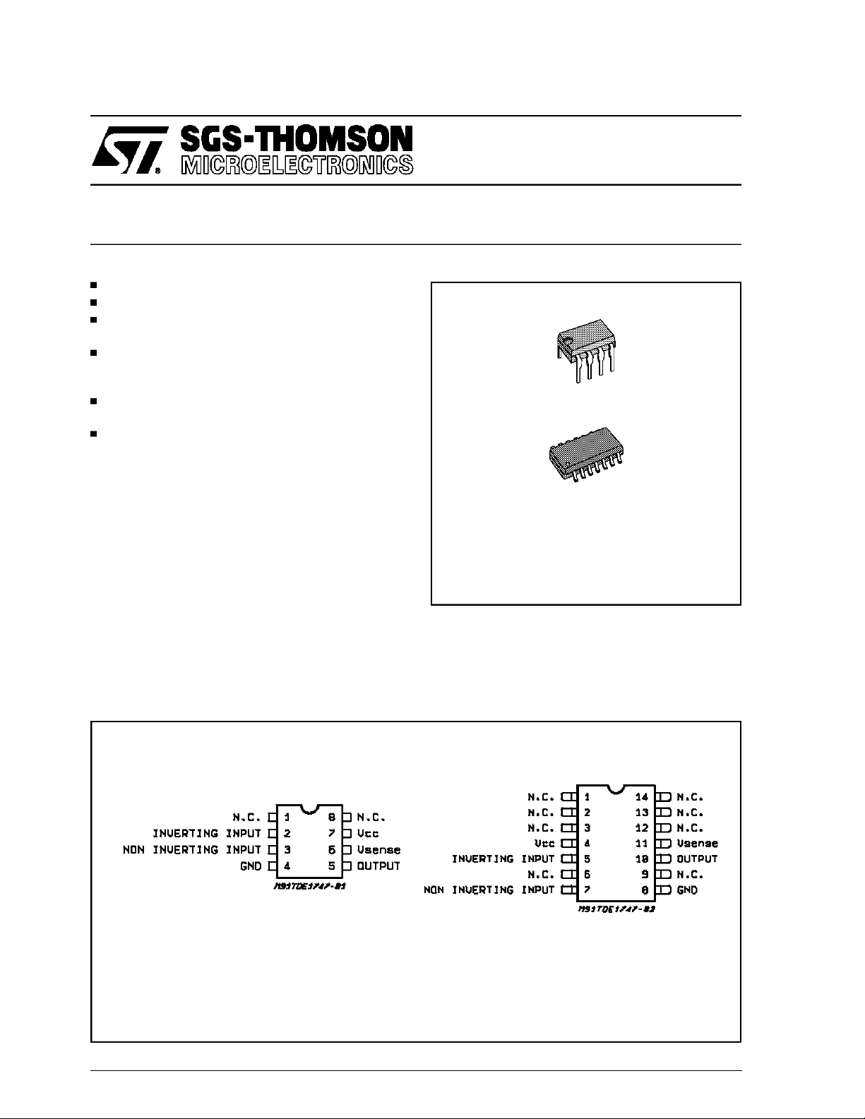
PIN CONNECTIONS (Topview)
CC
TDE1747
TDF1747
Minidip (DP)
SO14 (FP)
ORDERING NUMBERS:
TDE1747DP
TDE1747FP
TDF1747DP
The device operates over a wide range of supply
voltages from standard ± 15 V operationalamplifier supplies down to the single + 12 V or + 24
usedfor industrial electronicsystems.
Minidip
November 1991
This is advanced information on anew product now in development or undergoing evaluation. Details are subject tochange without notice.
SO14
1/11
Page 2
TDE1747 - TDF1747
ABSOLUTE MAXIMUM RATINGS
Symbol Parameter Value Unit
V
CC
V
ID
V
I
I
O
P
tot
T
stg
T
oper
(*) 60V, tâ 10ms
THERMAL CHARACTERISTICS
Symbol Parameter Value Unit
R
th(j-c)
R
th(j-a)
R
th
R
th
Supply Voltage 50 * V
Differantial Input Voltage 50 V
Input Voltage 50 V
Output Current 1 A
Power Dissipation (T
=+25°C) Internally Limited W
amb
Storage Temperature Range – 65 to + 150 °C
Operating Ambient Temperature Range
TDE1747
TDF1747
–25to+85
–40to+85
Maximum Junction-caseThermal Resistance 50 °C/W
Maximum Junction-ambient Thermal Resistance 120 °C/W
Junction-ceramic Substrate (case glued to substrate) SO14 90 °C/W
Junction-ceramic Substrate (case glued to substrate, substrate temperature
maintened constant)
65 °C/W
SO14
°C
°C
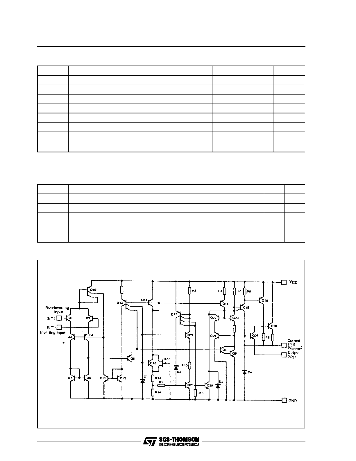
SCHEMATIC DIAGRAM
2/11
Page 3
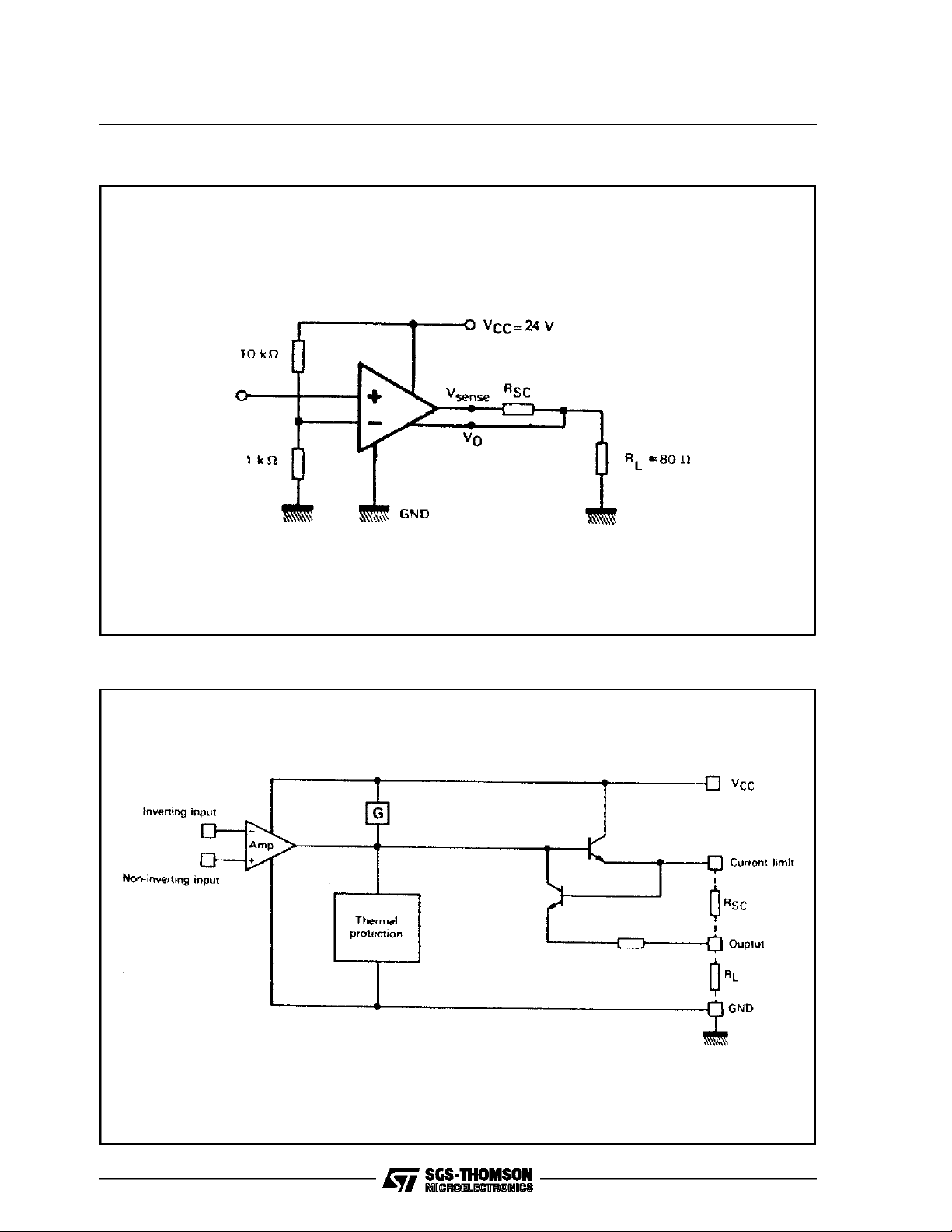
TEST CIRCUIT
TDE1747 - TDF1747
SIMPLIFIEDCIRCUIT
3/11
Page 4
TDE1747 - TDF1747
ELECTRICAL CHARACTERISTICS Tj= – 25 to +85 °C, VCC= 8 to 45 V, unless otherwise specified
(note 1).
Symbol Parameter Min. Typ. Max. Unit
V
IO
I
IB
I
CC
Input Offset Voltage - (note 2) – 2 50 mV
Input Bias Current – 0.1 1.5 mA
Supply Current (VCC= + 24 V, IO=0)
High Level
Low Level
–
–
4
2
6
4
mA
mA
V
I(max)
I
SC
V
CC–VO
I
OL
Notes :
1) For operating at high temperature, the TDE/TDF1747, must be derated based on a + 150 C maximum junction temperature and a
junction-ambient thermal resistance of 120 °C/W for Minidip and 100 °C/W for the SO14.
2) The offsetvoltage given isthe maximum value of input voltage required to drive the output voltage within 2 V of the ground or the supply
voltage.
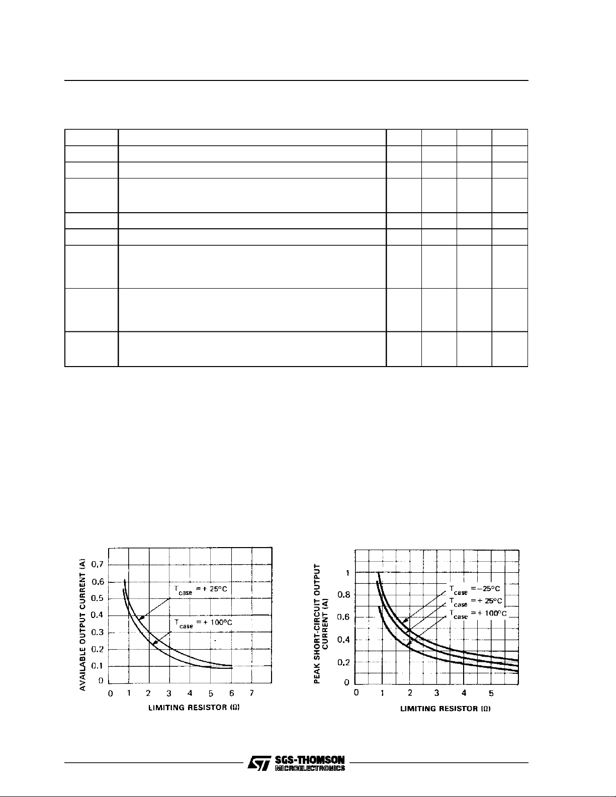
Figure1: Available Output Current vs. Limiting
Common-mode Input Voltage Range 2 – VCC–2 V
Short-circuit Current Limit
=+25°C, VCC= + 24)
(T
amb
= 1.5 Ω TDE1747
R
SC
= ∞
R
SC
–
–
480
35
–
50
Output Saturation Voltage(output high)
(R
=0, VI+–VI– ≥ 50 mV)
SC
= 300 mA, Tj=+25°C
I
O
= + 150 °C
T
j
–
1.15
–
1.05
1.4
1.3
Low Level Output Current
=0, VCC=+24V)
(V
O
=+25°C – 0.01 10 µA
T
j
Figure2: Peak Short-circuit Output Current vs.
Resistor
LimitingResistor
mA
mA
V
V
4/11
Page 5

TDE1747 - TDF1747
Figure3: Short-circuitCurrent vs. Case
Temperature
Figure5: Output Current vs. Output Saturation
Voltage
Figure4: MinimumLimiting Resistor Value vs.
Supply Voltage
Figure6: SupplyCurrent vs. Supply Voltage
Figure7: SupplyCurrent vs. Junction
Temperature
Figure8: Safe OperatingArea (non repetitive
surge)
5/11
Page 6

TDE1747 - TDF1747
Figure9: Response Time
TYPICALAPPLICATIONS
Figure10: BaseCircuit
6/11
Page 7

Figure11: OutputCurrent Extension (5A)
TDE1747 - TDF1747
Figure12: Driving Low ImpedanceRelays (I
The device in theabove applicationoperates at: VCC= +45V, IO=300mA with aheatsink such thatR
an outputvoltage of V
supply voltage.
duringthecurrent cut off time, which is decreased by the zener diode.Thisvoltage must be≤ to the maximum
CC=VZ
=300mA)
O
≤ 80°C/W. The device supports
th(j-a)
7/11
Page 8

TDE1747 - TDF1747
Figure13: Waveforms
(FIGURE13a)
8/11
(FIGURE 13b)
Page 9

SO14PACKAGE MECHANICAL DATA
TDE1747 - TDF1747
DIM.
MIN. TYP. MAX. MIN. TYP. MAX.
A 1.75 0.069
a1 0.1 0.25 0.004 0.009
a2 1.6 0.063
b 0.35 0.46 0.014 0.018
b1 0.19 0.25 0.007 0.010
C 0.5 0.020
c1 45 (typ.)
D 8.55 8.75 0.336 0.344
E 5.8 6.2 0.228 0.244
e 1.27 0.050
e3 7.62 0.300
F 3.8 4.0 0.15 0.157
L 0.4 1.27 0.016 0.050
M 0.68 0.027
S 8 (max.)
mm inch
9/11
Page 10

TDE1747 - TDF1747
MINIDIP PACKAGE MECHANICAL DATA
DIM.
MIN. TYP. MAX. MIN. TYP. MAX.
A 3.32 0.131
a1 0.51 0.020
B 1.15 1.65 0.045 0.065
b 0.356 0.55 0.014 0.022
b1 0.204 0.304 0.008 0.012
D 10.92 0.430
E 7.95 9.75 0.313 0.384
e 2.54 0.100
e3 7.62 0.300
e4 7.62 0.300
F 6.6 0.260
I 5.08 0.200
L 3.18 3.81 0.125 0.150
Z 1.52 0.060
mm inch
10/11
Page 11

TDE1747 - TDF1747
Information furnished is believed to be accurate and reliable. However,SGS-THOMSON Microelectronics assumes no responsibility for the
consequences of use of such information nor for any infringement of patents or other rights of third parties whichmay resultfrom its use. No
license is granted by implication or otherwise under any patent or patent rights of SGS-THOMSON Microelectronics. Specifications mentioned in this publication are subject to change without notice. This publication supersedes and replaces all information previously supplied.
SGS-THOMSON Microelectronics products are not authorized for use as critical components in lifesupport devices or systems without express writtenapproval of SGS-THOMSON Microelectronics.
1994 SGS-THOMSON Microelectronics - All RightsReserved
SGS-THOMSON Microelectronics GROUPOF COMPANIES
Australia - Brazil - France - Germany - Hong Kong - Italy - Japan- Korea - Malaysia -Malta - Morocco - The Netherlands - Singapore-
Spain - Sweden - Switzerland - Taiwan - Thaliand- United Kingdom - U.S.A.
11/11
 Loading...