

Page 1
0.5A OUTPUTCURRENT
LOW SIDE OR HIGH SIDE SWITCH CON-
FIGURATION
6V TO 48V SUPPLY VOLTAGERANGE
OVERLOADANDSHORT CIRCUIT PROTEC-
TIONS
INTERNALVOLTAGECLAMPING
SUPPLY AND OUTPUT REVERSAL PRO-
TECTION
THERMALSHUTDOWN
GNDAND V
OPENWIRE PROTECTION
S
ADJUSTABLEDELAYAT SWITCHON
INDICATORSTATUSLED DRIVER
+5V REGULATEDAUX. VOLTAGE
HIGHBURST IMMUNITY
DESCRIPTION
The TDE1707BFP is a 0.5A Integrated Power
Switch with up to 48V Power supply capability.
Two output configurationsare possible:
- Loadto Gnd.(High Side Mode)
- Loadto V
(Lowside Mode)
S
Especially dedicated to proximitydetectors, its in-
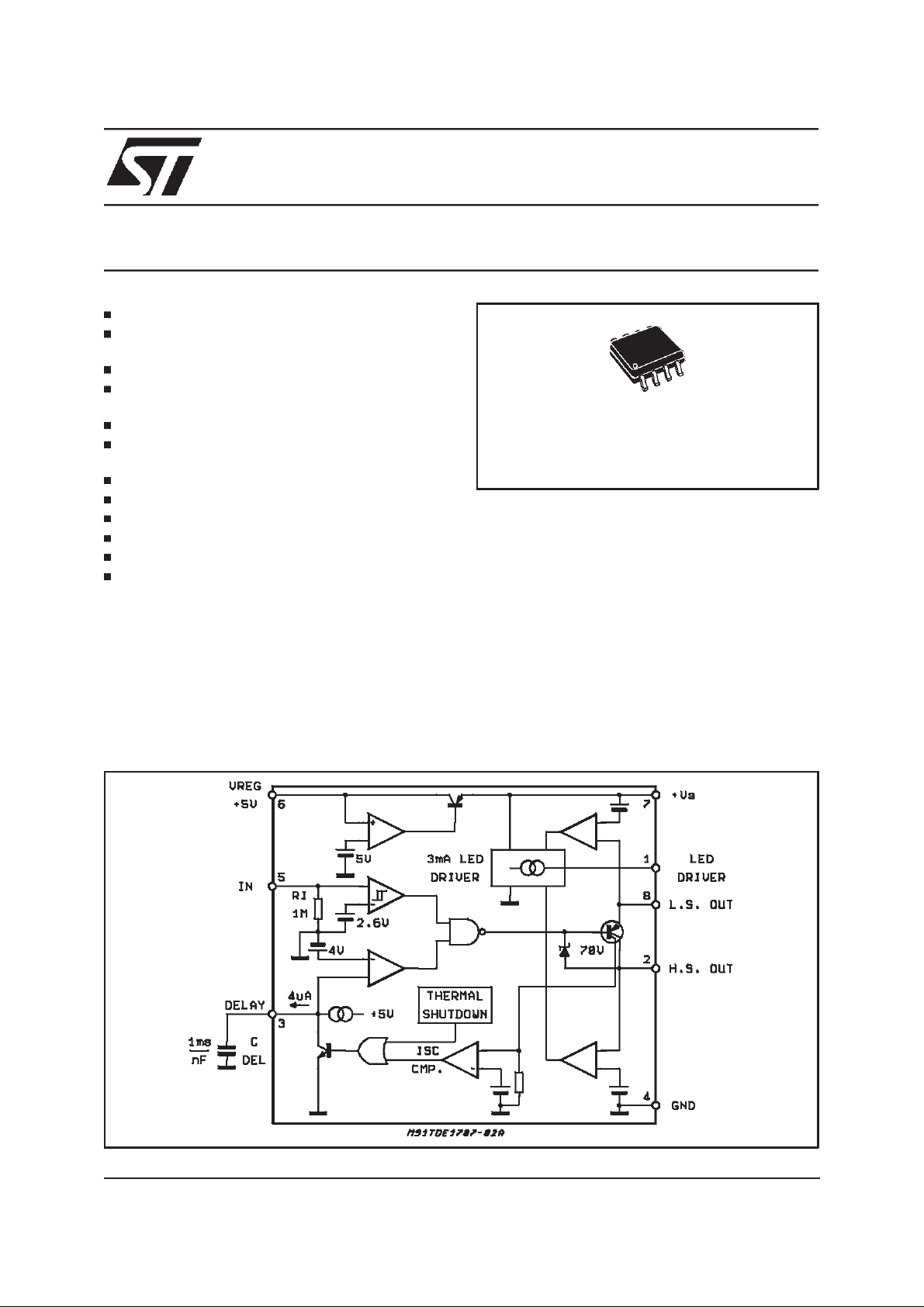
BLOCK DIAGRAM
TDE1707BFP
INTELLIGENTPOWER SWITCH
PRODUCT PREVIEW
SO8
ORDERING NUMBER: TDE1707BFP
ternal +5V supply can be used to supply external
circuits (See also AN495/0692). A signal is internally generatedto block the In signal, and prevent
activation of the output switch, as long as an abnormal condition is detected. The power-ontransition, as well as the chip overtemperature and
the output overcurrent, concurr to the generation
of such signal. A minimum delay of 25µs (Typ.
value) is added to the trailing edge of suchsignal
to ensure that a stable normal situation is present
when the signal disappears. The delay (of the disapperance of the block signal; no delay at its on
set) can be further increased connecting a capacitor between pin3 and ground. It can drive resistive or inductiveloads.
July 1999
This is preliminary information on a new product now in development or undergoing evaluation. Details are subject to change without notice.
1/6
Page 2
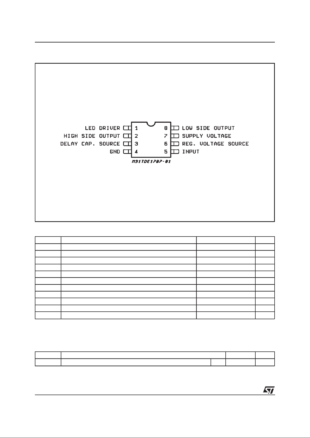
TDE1707BFP
PIN CONNECTION (Top view)
ABSOLUTE MAXIMUM RATINGS
Symbol Parameter Value Unit
Supply Voltage 50 V
S
Supply Reverse Voltage 50 V
Sr
Output Current internally limited A
O
Regulated Voltage Pin 0 to 7 V
reg
Delay Cap. Surce Pin 0 to 5 V
Output Diff. Voltage 55 V
O
Input Voltage -10 to 50 V
i
Operating Temperature Range -25 to +85 °C
op
Storage Temperature -55 to 150
stg
Power Dissipation internally limited W
tot
Energy Induct. Load 150 mJ
l
V
V
V
I
V
delay
V
V
T
T
P
E
THERMAL DATA
Symbol Description Value Unit
R
th j-amb
Thermal Resistance Junction-ambient Max. 150
°
C/W
°
C
2/6
Page 3

TDE1707BFP
ELECTRICALCHARACTERISTICS(VS= 24V; Tj= –25 to +85°C,unless otherwise specified)
Symbol Parameter Test Condition Min. Typ. Max. Unit
7 Supply Voltage 6 48 V
V
s
7 Supply Reverse Current VSR= –48V 1.5 mA
I
sr
7 QuiescentCurrent I
I
q
reg=Iled
V
8/2 Output Current Vs= 6V to 32V 500 mA
I
o
8/2 Output Current Vs = 32V to 48V 300 mA
I
o
8/2 Output Voltage Drop V
V
sat
8/2 Output Voltage Drop V8-2 Io = 300mA 1.5 V
V
sat
8/2 Short Circuit Current 0.7 1.5 A
I
sc
8/2 InternalVoltage Clamp ICL= 10mA 55 70 V
V
cl
8/2 Output Leakage 0 (Pin 2)
I
olk
8-2
Io= 500mA 1.1 1.6 V
V
5 Input Voltage Threshold 2 3 V
V
ith
5 Input Threshold Hysteresis 300 mV
V
ihis
5 Input Current Vi=5V 2 5
I
lk
6 Regulated Output Voltage I
V
reg
6 Short Circuit Regulated 6 30 50 mA
I
scr
6 Ouput Regulator Current Vs= 35V
I
reg
reg
V
1 Current Surce Sink Led Driver Output ON (±)234mA
I
old
1 Voltage Drop Led Driver Ios= 2mA (±) 1.2 1.6 V
V
old
Oldlk 1 Lead Driver (off) Leak. V
3 Del. Cap. Charge Current TJ=25°C246µA
I
dch
3 Delay Voltage Trigger TJ=25°C4V
V
dth
= 6 to 48V
S
=0;Vi< 2V;
1.5 mA
100 300
< 2V; Vo= 0 to Vs(Pin 8)
i
100
< 5mA 4.5 5 5.5 V
6
= 48V
s
< 2V; RL<1KΩ 10 µA
i
4
µA
µA
µ
mA
mA
A
APPLICATION INFORMATION (See Application
Circuit)
The LED driver tells the outputstatus.
It can source or sink current (I
old typ
= 3mA), according to the output configurationchosen.
The thresholds, represented by the output comparator in the Block Diagram, are set at about
1.5V - 2V.
For instance, in the High Side Load case of the
ApplicationCircuit, when the voltage on pin 8 (the
output) differs from V
is sensed in ”OFF” state and the LED driver is
disabled.
If insteadpin 8 differsfrom V
output comparator threshold value plus the drop
voltage on the LED), then the output is sensed
”ON” and the driver will force the current on the
LED.
DYNAMICCHARACTERISTICS (VS= 24V; RL=48Ω;TJ=25°C)
t
t
t
don
t
d min
on
off
Propagation Turn on Time Vi= 0 to 5V 15 µs
Propagation Turn off Time Vi= 5 to 0V 15 µs
Delayed Turn on Time / nF
Delay Capacitor
Minimum Delayed t
on
Delay Capacitor = 0
lessthan 1.5V, the output
CC
morethan 3V(the
CC
0.65 1 2 ms
25
µ
s
3/6
Page 4

TDE1707BFP
APPLICATIONCIRCUIT Figure1: InputThresholds Voltage vs.
Temperature(V
= 24V)
S
Figure 2: SaturationVoltage vs. Temperature
= 24V; IO= 500mA)
(V
S
Figure3: QuiescentCurrent) vs.Temperature
= 24V)
(V
S
4/6
Page 5

TDE1707BFP
DIM.
MIN. TYP. MAX. MIN. TYP. MAX.
A 1.75 0.069
a1 0.1 0.25 0.004 0.010
a2 1.65
a3 0.65 0.85 0.026 0.033
b 0.35 0.48 0.014 0.019
b1 0.19 0.25 0.007 0.010
C 0.25 0.5 0.010 0.020
c1 45° (typ.)
D (1) 4.8 5.0 0.189 0.197
E 5.8 6.2 0.228 0.244
e 1.27 0.050
e3 3.81 0.150
F (1) 3.8 4.0 0.15 0.157
L 0.4 1.27 0.016 0.050
M 0.6 0.024
S8°(max.)
(1) D andF donot include mold flashor protrusions. Moldflash or
potrusionsshallnot exceed 0.15mm (.006inch).
mm inch
0.065
OUTLINE AND
MECHANICAL DATA
SO8
5/6
Page 6

TDE1707BFP
Information furnished is believed tobe accurate and reliable. However, STMicroelectronics assumes no responsibility for the consequences
of use of such information nor for any infringement of patents or other rights of third parties which may result from its use. No license is
granted by implication or otherwise under any patent or patent rights of STMicroelectronics. Specification mentioned in this publication are
subject to change without notice. This publication supersedes and replaces all information previously supplied. STMicroelectronics products
are not authorized for use as critical components in life support devices or systems without express written approval of STMicroelectronics.
The ST logo is a registered trademark of STMicroelectronics
1999 STMicroelectronics – Printed in Italy – AllRights Reserved
STMicroelectronics GROUP OF COMPANIES
Australia - Brazil - China- Finland - France - Germany - Hong Kong - India - Italy - Japan - Malaysia - Malta - Morocco -
Singapore - Spain - Sweden - Switzerland - United Kingdom - U.S.A.
http://www.st.com
6/6
 Loading...