

Datasheet TDA6403AM-C1, TDA6402M-C2, TDA6402AM-C2, TDA6402AM-C1-M1, TDA6403M-C3 Datasheet (Philips)
...Page 1

DATA SH EET
Product specification
Supersedes data of 1998 Jul 28
File under Integrated Circuits, IC02
2000 Jan 24
INTEGRATED CIRCUITS
TDA6402; TDA6402A; TDA6403;
TDA6403A
5 V mixers/oscillators and
synthesizers for cable TV and VCR
2-band tuners
Page 2

2000 Jan 24 2
Philips Semiconductors Product specification
5 V mixers/oscillators and synthesizers for
cable TV and VCR 2-band tuners
TDA6402; TDA6402A;
TDA6403; TDA6403A
FEATURES
• Single-chip 5 V mixer/oscillator and synthesizer for
cable TV and VCR tuners
• Synthesizer function compatible with existing TSA5526
• Universal bus protocol (I2C-bus or 3-wire bus)
– Bus protocol for 18 or 19-bit transmission (3-wire
bus)
– Extraprotocolfor 27-bit transmission(testmodes and
features for 3-wire bus)
– Address + 4 data bytes transmission (I2C-bus ‘write’
mode)
– Address + 1 status byte (I2C-bus ‘read’ mode)
– 4 independent I2C-bus addresses.
• 1 PNP buffer for UHF band selection (25 mA)
• 3 PNP buffers for general purpose, e.g. 2 VHF
sub-bands, FM sound trap (25 mA)
• 33 V tuning voltage output
• In-lock detector
• 5-step A/D converter (3 bits in I2C-bus mode)
• 15-bit programmable divider
• Programmable reference divider ratio (512, 640 or
1024)
• Programmable charge pump current (60 or 280 µA)
• Programmable automatic charge pump current switch
• Varicap drive disable
• Mixer/oscillator function compatible with existing
TDA5732
• Balanced mixer with a common emitter input for VHF
(single input)
• Balanced mixer with a common base input for UHF
(balanced input)
• 2-pin common emitter oscillator for VHF
• 4-pin common emitter oscillator for UHF
• IF preamplifier with asymmetrical 75 Ω output
impedance to drive a low-ohmic impedance (75 Ω)
• Low power
• Low radiation
• Small size
• TheTDA6402A andTDA6403Adifferfrom theTDA6402
and TDA6403 by the UHF port protocol in the I2C-bus
mode (see Tables 3 and 4).
APPLICATIONS
• Cable tuners for TV and VCR (switched concept for
VHF)
• Recommended RF bands for the USA:
55.25 to 133.25 MHz, 139.25 to 361.25 MHz and
367.25 to 801.25 MHz.
GENERAL DESCRIPTION
The TDA6402, TDA6402A, TDA6403 and TDA6403A are
programmable2-band mixers/oscillatorsand synthesizers
intended for VHF/UHF cable tuners (see Fig.1).
The devices include two double balanced mixers and two
oscillators for the VHF and UHF band respectively, an IF
amplifier and a PLL synthesizer. The VHF band can be
split-up into two sub-bands using a proper oscillator
application and a switchable inductor. Two pins are
available between the mixer output and the IF amplifier
input to enable IF filtering for improved signal handling.
Four PNP ports are provided. Band selection is provided
by using pin PUHF. When PUHF is ‘ON’, the UHF
mixer-oscillator is active andthe VHFband isswitched off.
When PUHF is ‘OFF’, the VHF mixer-oscillator is active
and the UHF band is ‘OFF’. PVHFL and PVHFH areused
to select the VHF sub-bands. FMST is a general purpose
port, that can be used to switch an FM sound trap. When
itis used,thesum ofthe collector currentshas tobelimited
to 30 mA.
The synthesizer consists of a divide-by-eight prescaler, a
15-bit programmable divider, a crystal oscillator and its
programmable reference divider and a phase/frequency
detector combined with a charge pump which drives the
tuning amplifier, including 33 V output (V33) at pin VT.
Depending on the reference divider ratio (512, 640 or
1024), the phase comparator operates at 7.8125 kHz,
6.25 kHz or 3.90625 kHz with a 4 MHz crystal.
Page 3

2000 Jan 24 3
Philips Semiconductors Product specification
5 V mixers/oscillators and synthesizers for
cable TV and VCR 2-band tuners
TDA6402; TDA6402A;
TDA6403; TDA6403A
The device can be controlled according to the I2C-bus
format or 3-wire bus format depending on the voltage
applied to pin SW (see Table 2). In the 3-wire bus mode
(SW = HIGH), pin LOCK/ADC is the LOCK output.
The LOCK output is LOW when the PLL loop is locked.
In the I2C-bus mode(SW = LOW), the lockdetector bit FL
is set tologic 1 when the loop is locked and is read on the
SDA line (Status Byte; SB) during a READ operation in
I2C-bus mode only. The Analog-to-Digital Converter
(ADC) input isavailable on pin LOCK/ADC for digitalAFC
control in the I2C-bus mode only. The ADC code is read
during a READ operation on the I2C-bus (see Table 11).
In test mode,pin LOCK/ADC isused as aTEST outputfor
f
REF
and1⁄2f
DIV
,in bothI2C-busmode and3-wirebus mode
(see Table 7).
When the automatic charge pump current switch mode is
activated and when the loop is phase-locked, the charge
pumpcurrent valueisautomatically switchedto LOW.This
action is taken to improve the carrier-to-noise ratio.
The status of this feature can be read in the ACPS flag
during a READ operation on the I2C-bus (see Table 9).
I
2
C-bus mode (SW = GND)
Five serial bytes (including address byte) are required to
address the device, select the VCO frequency, program
the four ports, set the charge pump current and set the
reference divider ratio. The device has four independent
I2C-bus addresses which can be selected by applying a
specific voltage on input CE (see Table 6).
3-wire bus mode (SW = OPEN or VCC)
Data is transmitted to the devices during a HIGH-level on
inputCE (enableline). The deviceis compatiblewith 18-bit
and19-bit dataformats,as showninFigs 4 and 5. Thefirst
four bits are used to program the PNP ports and the
remaining bits control the programmable divider. A 27-bit
data format may also be used to set the charge pump
current, the reference divider ratio and for test purposes
(see Fig.6).
It is not allowed to address the devices with words whose
length is different from 18, 19 or 27 bits.
Table 1 Data word length for 3-wire bus
Note
1. The selectionof the referencedivider is givenby an automaticidentification of thedata word length.When the 27-bit
format is used, the reference divider is controlled by RSA and RSB bits (see Table 8). More details are given in
Chapter “PLL functional description”, Section “3-wire bus mode (SW = OPEN or V
CC
)”.
TYPE NUMBER DATA WORD REFERENCE DIVIDER
(1)
FREQUENCY STEP
TDA6402; TDA6402A; TDA6403; TDA6403A 18-bit 512 62.50 kHz
TDA6402; TDA6402A; TDA6403; TDA6403A 19-bit 1024 31.25 kHz
TDA6402; TDA6402A; TDA6403; TDA6403A 27-bit programmable programmable
Page 4
2000 Jan 24 4
Philips Semiconductors Product specification
5 V mixers/oscillators and synthesizers for
cable TV and VCR 2-band tuners
TDA6402; TDA6402A;
TDA6403; TDA6403A
QUICK REFERENCE DATA
Measured over full voltage and temperature ranges; unless otherwise specified.
Notes
1. One buffer ‘ON’, Io= 25 mA; two buffers ‘ON’, maximum sum of Io= 30 mA.
2. The power dissipation is calculated as follows:
ORDERING INFORMATION
SYMBOL PARAMETER CONDITIONS MIN. TYP. MAX. UNIT
V
CC
supply voltage operating 4.5 5 5.5 V
I
CC
supply current all PNP ports are ‘OFF’ − 71 − mA
f
XTAL
crystal oscillator input frequency 3.2 4.0 4.48 MHz
I
o(PNP)
PNP port output current note 1 −−30 mA
P
tot
total power dissipation note 2 −−490 mW
T
stg
IC storage temperature −40 − +150 °C
T
amb
ambient temperature −20 − +85 °C
f
RF
RF frequency VHF band 55.25 − 361.25 MHz
UHF band 367.25 − 801.25 MHz
G
V
voltage gain VHF band − 19 − dB
UHF band − 29 − dB
NF noise figure VHF band − 8.5 − dB
UHF band − 9 − dB
V
o
output voltage causing 1% cross
modulation in channel
VHF band − 108 − dBµV
UHF band − 108 − dBµV
TYPE NUMBER
PACKAGE
NAME DESCRIPTION VERSION
TDA6402M;
TDA6402AM
SSOP28 plastic shrink small outline package; 28 leads; body width 5.3 mm SOT341-1
TDA6403M;
TDA6403AM
SSOP28 plastic shrink small outline package; 28 leads; body width 5.3 mm SOT341-1
P
tot
V
CCICCIo
–()V
CE(sat PNP)Io
1
2
-- -
V33
2
22 kΩ
-----------------------
+×+×=
Page 5
2000 Jan 24 5
Philips Semiconductors Product specification
5 V mixers/oscillators and synthesizers for
cable TV and VCR 2-band tuners
TDA6402; TDA6402A;
TDA6403; TDA6403A
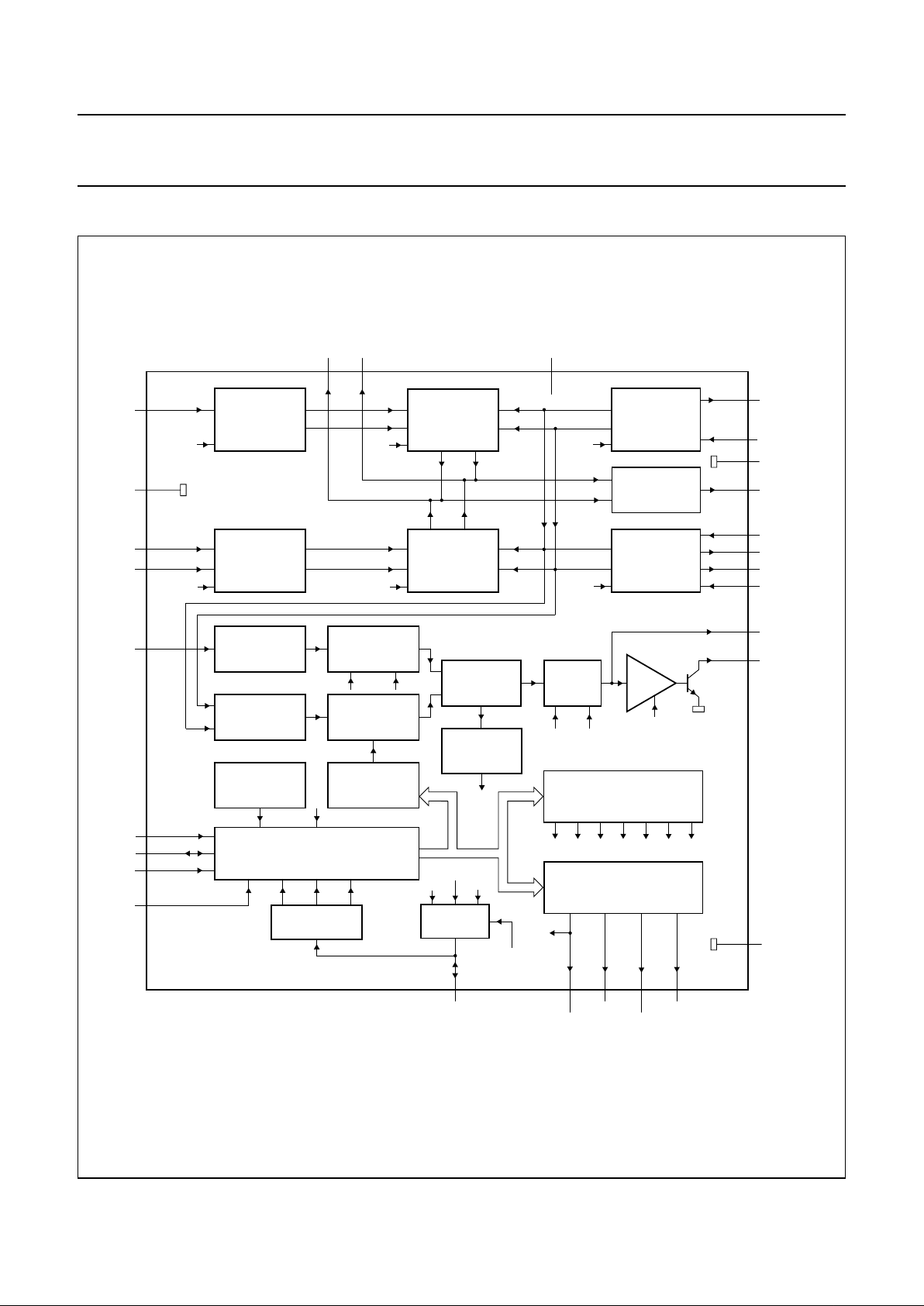
BLOCK DIAGRAM
Fig.1 Block diagram.
The pin numbers in parenthesis represent the TDA6403 and TDA6403A.
handbook, full pagewidth
MGE692
PRESCALER
DIVIDE BY
512, 640, 1024
XTAL
OSCILLATOR
4 MHz
15-BIT
PROGRAMMABLE
DIVIDER
15-BIT
FREQUENCY
REGISTER
PRESCALER
DIVIDE BY 8
POWER-DOWN
DETECTOR
PHASE
COMPARATOR
IN LOCK
DETECTOR
CHARGE
PUMP
OPAMP
FL
T0, T1, T2 CP
OS
CP T2 T1 T0 RSA RSB OS
CONTROL
REGISTER
FL
I
2
C / 3-WIRE BUS TRANSCEIVER
3-BIT A/D
CONVERTER
PORT
REGISTER
UHF VHFH VHFL FMST
FL
f
REF
f
REF
1/2f
DIV
f
DIV
GATE
RF INPUT
VHF
VHF
MIXER
VHF
OSCILLATOR
RF INPUT
UHF
UHF
MIXER
UHF
OSCILLATOR
IF
PREAMPLIFIER
BS
BS
BS
BSBS
BS
BS
T0, T1, T2
RSA RSB
VHFIN
RFGND
UHFIN1
UHFIN2
XTAL
CL
DA
SW
CE/AS
IFFIL1 IFFIL2
V
CC
VHFOSCOC
VHFOSCIB
OSCGND
IFOUT
UHFOSCIB2
UHFOSCOC2
UHFOSCOC1
UHFOSCIB1
CP
VT
GND
FMST
PVHFL
PVHFH
PUHF
LOCK/ADC
3 (26)
4 (25)
1 (28)
2 (27)
18 (11)
14 (15)
13 (16)
11 (18)
12 (17)
15 (14)
9 (20)
8 (21)
7 (22)
10 (19)
(8) 21
(12) 17
(13) 16
(4) 25
(3) 26
(2) 27
(1) 28
(9) 20
(6) 23
(7) 22
(5) 24
19 (10)
6 (23)
5 (24)
SCL
SDA
SW
CE/AS
TDA6402
TDA6402A
TDA6403
TDA6403A
Page 6

2000 Jan 24 6
Philips Semiconductors Product specification
5 V mixers/oscillators and synthesizers for
cable TV and VCR 2-band tuners
TDA6402; TDA6402A;
TDA6403; TDA6403A
PINNING
SYMBOL
PIN
DESCRIPTION
TDA6402;
TDA6402A
TDA6403;
TDA6403A
UHFIN1 1 28 UHF RF input 1
UHFIN2 2 27 UHF RF input 2
VHFIN 3 26 VHF RF input
RFGND 4 25 RF ground
IFFIL1 5 24 IF filter output 1
IFFIL2 6 23 IF filter output 2
PVHFL 7 22 PNP port output, general purpose (e.g. VHF low sub-band)
PVHFH 8 21 PNP port output, general purpose (e.g. VHF high sub-band)
PUHF 9 20 PNP port output, UHF band
FMST 10 19 PNP port output, general purpose (e.g. FM sound trap)
SW 11 18 bus mode selection input (I
2
C-bus/3-wire bus)
CE/AS 12 17 Chip Enable/Address Selection input
DA 13 16 serial data input/output
CL 14 15 serial clock input
LOCK/ADC 15 14 lock detector output (3-wire bus)/ADC input (I
2
C-bus)
CP 16 13 charge pump output
VT 17 12 tuning voltage output
XTAL 18 11 crystal oscillator input
V
CC
19 10 supply voltage
IFOUT 20 9 IF output
GND 21 8 digital ground
VHFOSCIB 22 7 VHF oscillator input base
OSCGND 23 6 oscillator ground
VHFOSCOC 24 5 VHF oscillator output collector
UHFOSCIB1 25 4 UHF oscillator input base 1
UHFOSCOC1 26 3 UHF oscillator output collector 1
UHFOSCOC2 27 2 UHF oscillator output collector 2
UHFOSCIB2 28 1 UHF oscillator input base 2
Page 7

2000 Jan 24 7
Philips Semiconductors Product specification
5 V mixers/oscillators and synthesizers for
cable TV and VCR 2-band tuners
TDA6402; TDA6402A;
TDA6403; TDA6403A
Fig.2 Pin configurationfor TDA6402 and
TDA6402A.
handbook, halfpage
UHFIN1
UHFIN2
VHFIN
RFGND
IFFIL1
IFFIL2
PVHFL
PVHFH
PUHF
FMST
SW
CE/AS
DA
CL
UHFOSCIB2
UHFOSCOC2
UHFOSCOC1
UHFOSCIB1
OSCGND
VHFOSCIB
VHFOSCOC
GND
IFOUT
V
CC
XTAL
VT
CP
LOCK/ADC
1
2
3
4
5
6
7
8
9
10
11
12
13
28
27
26
25
24
23
22
21
20
19
18
17
16
1514
TDA6402
TDA6402A
MGE690
Fig.3 Pin configurationfor TDA6403 and
TDA6403A.
handbook, halfpage
UHFIN1
UHFIN2
VHFIN
RFGND
IFFIL1
IFFIL2
PVHFL
PVHFH
PUHF
FMST
SW
CE/AS
DA
CL
UHFOSCIB2
UHFOSCOC2
UHFOSCOC1
UHFOSCIB1
OSCGND
VHFOSCIB
VHFOSCOC
GND
IFOUT
V
CC
XTAL
VT
CP
LOCK/ADC
1
2
3
4
5
6
7
8
9
10
11
12
13
28
27
26
25
24
23
22
21
20
19
18
17
16
1514
TDA6403
TDA6403A
MGE691
PLL FUNCTIONAL DESCRIPTION
The device is controlled via the I2C-bus or the 3-wire bus,
depending on the voltage applied on the SW input.
A HIGH-level on the SW input enables the 3-wire bus;
CE/AS, DA and CL inputs are used as enable (CE), data
and clock inputs respectively. A LOW-level on SW input
enables the I2C-bus; the CE/AS, DA and CL inputs are
used as address selection (AS), SDA and SCL input
respectively (see Table 2).
Table 2 Bus mode selection
SYMBOL
PIN
3-WIRE BUS MODE I2C-BUS MODE
TDA6402;
TDA6402A
TDA6403;
TDA6403A
SW 11 18 HIGH-level or OPEN LOW-level or GND
CE/AS 12 17 enable input address selection input
DA 13 16 data input serial data input
CL 14 15 clock input serial clock input
LOCK/ADC 15 14 LOCK/TEST output ADC input/TEST output
Page 8
2000 Jan 24 8
Philips Semiconductors Product specification
5 V mixers/oscillators and synthesizers for
cable TV and VCR 2-band tuners
TDA6402; TDA6402A;
TDA6403; TDA6403A
I2C-bus mode (SW = GND)
WRITE MODE; R/W = 0 (see Tables 3 and 4)
Data bytes can be sent to the device after the address
transmission (first byte). Four data bytes are needed to
fully program the device. The bus transceiver has an
auto-increment facility which permits the programming of
the device within one single transmission
(address + 4 data bytes).
The device can also be partially programmed providing
that the first data byte following the address is divider
byte 1 (DB1) or control byte (CB). The bits in the data
bytes aredefined inTables 3 and 4. The firstbit ofthe first
data byte transmitted indicates whether frequency data
(first bit = 0) or control and band-switch data (first bit = 1)
will follow.Until an I2C-bus STOPcommand is sent by the
controller,additional databytes canbe entered withoutthe
need to re-address the device. The frequency register is
loaded after the8th clock pulse of thesecond divider byte
(DB2), the control register is loaded after the 8th clock
pulse ofthe controlbyte (CB)and theband-switch register
is loaded after the 8th clock pulse of the band switch byte
(BB).
I2C-BUS ADDRESS SELECTION
The moduleaddress contains programmableaddress bits
(MA1 and MA0) which offer the possibility of having
several synthesizers(up to 4) inone system byapplying a
specific voltageon theCE input.The relationshipbetween
MA1 and MA0 and the input voltage applied to the CE
input is given in Table 6.
Table 3 I2C-bus data format, ‘write’ mode for the TDA6402 and TDA6403
Table 4 I
2
C-bus data format, ‘write’ mode for the TDA6402A and TDA6403A
NAME BYTE
BITS
ACK
MSB LSB
Address byte ADB 11000MA1MA0R/W=0A
Divider byte 1 DB1 0 N14 N13 N12 N11 N10 N9 N8 A
Divider byte 2 DB2 N7 N6 N5 N4 N3 N2 N1 N0 A
Control byte CB 1 CP T2 T1 T0 RSA RSB OS A
Band-switch byte BB XXXXFMST PUHF PVHFH PVHFL A
NAME BYTE
BITS
ACK
MSB LSB
Address byte ADB 11000MA1MA0R/W=0A
Divider byte 1 DB1 0 N14 N13 N12 N11 N10 N9 N8 A
Divider byte 2 DB2 N7 N6 N5 N4 N3 N2 N1 N0 A
Control byte CB 1 CP T2 T1 T0 RSA RSB OS A
Band-switch byte BB XXXXPUHF FMST PVHFH PVHFL A
Page 9
2000 Jan 24 9
Philips Semiconductors Product specification
5 V mixers/oscillators and synthesizers for
cable TV and VCR 2-band tuners
TDA6402; TDA6402A;
TDA6403; TDA6403A
Table 5 Description of symbols used in Tables 3 and 4
Table 6 Address selection (I
2
C-bus mode)
Table 7 Test modes
Notes
1. This is the default mode at power-on reset.
2. The ADCinput cannot beused when these testmodes are active;see Section “Read mode;R/W = 1 (see Table 9)”
for more information.
SYMBOL DESCRIPTION
A acknowledge
MA1, MA0 programmable address bits (see Table 6)
N14 to N0 programmable divider bits; N = N14 × 2
14
+ N13 × 213+ ... + N1 × 21+N0
CP charge pump current:
CP=0=60µA
CP = 1 = 280 µA (default)
T2, T1,T0 test bits (see Table 7)
RSA, RSB reference divider ratio select bits (see Table 8)
OS tuning amplifier control bit:
OS = 0; normal operation; tuning voltage is ‘ON’ (default)
OS = 1; tuning voltage is ‘OFF’ (high-impedance)
PVHFL, PVHFH, PUHF, FMST PNP ports control bits:
bit = 0; buffer n is ‘OFF’ (default)
bit = 1; buffer n is ‘ON’
X don’t care
MA1 MA0 VOLTAGE APPLIED ON CE INPUT (SW = GND)
0 0 0Vto0.1×V
CC
0 1 open or 0.2 × VCCto 0.3 × V
CC
1 0 0.4 × VCCto 0.6 × V
CC
1 1 0.9 × VCCto 1.0 × V
CC
T2 T1 T0 TEST MODES
0 0 0 automatic charge pump switched off
0 0 1 automatic charge pump switched on (note 1)
0 1 X charge pump is ‘OFF’
1 1 0 charge pump is sinking current
1 1 1 charge pump is sourcing current
100f
REF
is available on pin LOCK/ADC (note 2)
101
1
⁄
2
f
DIV
is available on pin LOCK/ADC (note 2)
Page 10
2000 Jan 24 10
Philips Semiconductors Product specification
5 V mixers/oscillators and synthesizers for
cable TV and VCR 2-band tuners
TDA6402; TDA6402A;
TDA6403; TDA6403A
Table 8 Reference divider ratio select bits
Note
1. X = don’t care.
RSA RSB REFERENCE DIVIDER RATIO FREQUENCY STEP (kHz)
X
(1)
0 640 6.25
0 1 1024 3.90625
1 1 512 7.8125
READ MODE; R/W = 1 (see Table 9)
Data canbe read from the device by settingthe R/W bit to
logic 1. After the slave address has been recognized, the
device generates an acknowledge pulse and the first data
byte (status byte) is transferred on the SDA line (MSB
first). Data is valid on the SDA line during a HIGH-level of
theSCL clocksignal. Asecond databyte canbe readfrom
the device if the microcontroller generates an
acknowledge on the SDA line (master acknowledge).
End of transmission will occur if no master acknowledge
occurs. The device will then release the data line to allow
the microcontroller to generate a STOP condition.
The PORflag isset to logic 1at power-on.Theflag isreset
when an end-of-data is detected by the device (end of a
READ sequence). Control of the loop is made possible
with the in-lock flag FL which indicates when the loop is
locked (FL = 1).
The automatic charge pump switch flag (ACPS) is LOW
when theautomatic chargepump switchmode is ‘ON’ and
the loop is locked. In other conditions, ACPS = 1.
When ACPS = 0, thecharge pump currentis forced to the
LOW value.
A built-in ADC is available on LOCK/ADC pin (I2C-bus
mode only). This converter can be used to apply AFC
informationto themicrocontroller fromthe IFsection ofthe
television.The relationshipbetween thebitsA2, A1andA0
is given in Table 11.
Table 9 Read data format
Note
1. MSB is transmitted first.
Table 10 Description of symbols used in Table 9
NAME BYTE
BITS
ACK
MSB
(1)
LSB
Address byte ADB 11000MA1MA0R/W=1A
Status byte SB POR FL ACPS 1 1 A2 A1 A0 −
SYMBOL DESCRIPTION
A acknowledge
POR power-on reset flag (POR = 1 at power-on)
FL in-lock flag (FL = 1 when the loop is locked)
ACPS automatic charge pump switch flag:
ACPS = 0; active
ACPS = 1; not active
A2, A1, A0 digital outputs of the 5-level ADC
Page 11

2000 Jan 24 11
Philips Semiconductors Product specification
5 V mixers/oscillators and synthesizers for
cable TV and VCR 2-band tuners
TDA6402; TDA6402A;
TDA6403; TDA6403A
Table 11 A to D converter levels (note 1)
Note
1. Accuracy is ±0.03 × V
CC
.
POWER-ON RESET
Table 12 Default bits at power-on reset
A2 A1 A0 VOLTAGE APPLIED ON ADC INPUT
1 0 0 0.60 × VCCto 1.00 × V
CC
0 1 1 0.45 × VCCto 0.60 × V
CC
0 1 0 0.30 × VCCto 0.45 × V
CC
0 0 1 0.15 × VCCto 0.30 × V
CC
0 0 0 0 to 0.15 × V
CC
NAME BYTE
BITS
MSB LSB
Address byte ADB 1 1 0 0 0 MA1 MA0 X
Divider byte 1 DB1 0 XXXXXXX
Divider byte 2 DB2 XXXXXXXX
Control byte CB 1 1 0 0 1 X 1 1
Band switch byte BB XXXX0000
The power-on detection threshold voltage V
POR
is set to
VCC= 2 V at room temperature. Below this threshold, the
device is reset to the power-on state.
At power-on state, the charge pump current is set to
280 µA, the tuning voltage outputis disabled, the test bits
T2, T1 and T0 are set to ‘001’ (automatic charge pump
switch ‘ON’) and RSB is set to logic 1.
PUHF is ‘OFF’, which means that the UHF oscillator and
the UHF mixer are switched off. Consequently, the VHF
oscillator andthe VHF mixer areswitched on. PVHFL and
PVHFH are ‘OFF’, which means that the VHF tank circuit
is working in the VHF I sub-band. The tuning amplifier is
switched off until the first transmission. In that case, the
tank circuit in VHF I is supplied with the maximum tuning
voltage. The oscillator is therefore working at the end of
the VHF I sub-band.
3-wire bus mode (SW = OPEN or VCC)
Duringa HIGH-levelon theCEinput (enableline), thedata
is clocked into the data register at the HIGH-to-LOW
transition of the clock. The first four bits control the PNP
ports and areloaded into the internal band switchregister
on the 5th rising edge of the clock pulse. The frequency
bits are loaded into the frequency register at the
HIGH-to-LOW transition of the chip enable line when an
18-bit or 19-bit data word is transmitted(see Figs 4 and 5).
When a27-bit data word istransmitted, the frequency bits
are loaded into the frequency register on the 20th rising
edge of the clock pulse and the control bits at the
HIGH-to-LOWtransition ofthechip enableline (seeFig.6).
Inthis mode,the referencedivider isgiven bythe RSA and
RSB bits (see Table 8). The test bits T2, T1 and T0, the
charge pump bit CP, the ratio select bit RSB and the OS
bit can only be selected or changed with a 27-bit
transmission. They remain programmed if an 18-bit or
19-bit transmission occurs. Only RSA is controlled by the
transmission length when the 18-bit or 19-bit format is
used. When an 18-bit data word is transmitted, the most
significant bit of the divider N14 is internally set to logic 0
and the RSA bit is set to logic 1. When a 19-bit data word
is transmitted, the RSA bit is set to logic 0.
A data word of less than 18 bits will not affect the
frequency register of the device. The definition of the bits
is unchanged compared to I2C-bus mode.
It is not allowed to address the devices with words whose
length is different from 18, 19 or 27 bits.
Page 12
2000 Jan 24 12
Philips Semiconductors Product specification
5 V mixers/oscillators and synthesizers for
cable TV and VCR 2-band tuners
TDA6402; TDA6402A;
TDA6403; TDA6403A
POWER-ON RESET
The power-on detection threshold voltage V
POR
is set to
VCC= 2 V at room temperature. Below this threshold, the
device is reset to the power-on state.
At power-on state, the charge pump current is set to
280 µA, the tuning voltage outputis disabled, the test bits
T2, T1 and T0 are set to ‘001’ (automatic charge pump
switch ‘ON’) and RSB is set to logic 1.
PUHF is ‘OFF’, which means that the UHF oscillator and
the UHF mixer are switched off. Consequently, the VHF
oscillator andthe VHF mixer areswitched on. PVHFL and
PVHFH are ‘OFF’, which means that the VHF tank circuit
is working in the VHF I sub-band. The tuning amplifier is
switched off until the first transmission. In that case, the
tank circuit in VHF I is supplied with the maximum tuning
voltage. The oscillator is therefore working at the end of
the VHF I sub-band.
If the first sequence transmitted to the device
has 18 or 19 bits, the reference divider ratio is set to 512
or 1024, depending on the sequence length.
If the sequence has 27 bits, the reference divider ratio is
fixed by RSA and RSB bits (see Table 8).
Fig.4 Normal mode; 18-bit data format (RSA = 1).
handbook, full pagewidth
MGE693
145 18
N13 N12 N11 N10 N9 N8 N7 N6 N5 N4 N3 N2 N1 N0
PUHF
FMST
PVHFH
PVHFL
INVALID
DATA
BAND SWITCH
DATA
FREQUENCY
DATA
INVALID
DATA
LOAD BAND SWITCH
REGISTER
LOAD FREQUENCY
REGISTER
DA
CL
CE
Page 13

2000 Jan 24 13
Philips Semiconductors Product specification
5 V mixers/oscillators and synthesizers for
cable TV and VCR 2-band tuners
TDA6402; TDA6402A;
TDA6403; TDA6403A
Fig.5 Normal mode; 19-bit data format (RSA = 0).
handbook, full pagewidth
MGE694
145 19
N13N14 N12 N11 N10 N9 N8 N7 N6 N5 N4 N3 N2 N1 N0
PUHF
FMST
PVHFH
PVHFL
INVALID
DATA
BAND SWITCH
DATA
FREQUENCY
DATA
INVALID
DATA
LOAD BAND SWITCH
REGISTER
LOAD FREQUENCY
REGISTER
DA
CL
CE
Fig.6 Test and features mode; 27-bit data format.
handbook, full pagewidth
MGE695
145 272019
N13N14 N12 N2 N1 N0 X CP T2 T1 T0 RSA RSB OS
PUHF
FMST
PVHFH
PVHFL
INVALID
DATA
BAND SWITCH
DATA
FREQUENCY
DATA
INVALID
DATA
LOAD BAND SWITCH
REGISTER
LOAD FREQUENCY
REGISTER
DA
CL
CE
TEST AND FEATURES
DATA
LOAD CONTROL
REGISTER
Page 14

2000 Jan 24 14
Philips Semiconductors Product specification
5 V mixers/oscillators and synthesizers for
cable TV and VCR 2-band tuners
TDA6402; TDA6402A;
TDA6403; TDA6403A
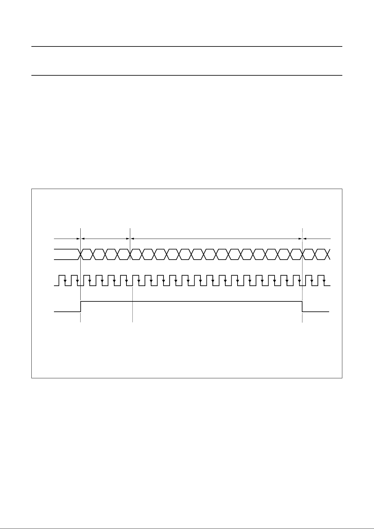
Fig.7 Timing diagram for 3-wire bus; DA, CL and CE.
handbook, full pagewidth
MGE696
t
HIGH
t
HD;DA
t
HD;ENDA
t
SU;DA
t
SU;ENCL
MSB LSB
DA
CL
CE
INVALID
DATA
INVALID
DATA
Fig.8 Timing diagram for 3-wire bus; CE and CL.
handbook, halfpage
MGE697
t
EN
t
HD;ENCL
CE
CL
Page 15

2000 Jan 24 15
Philips Semiconductors Product specification
5 V mixers/oscillators and synthesizers for
cable TV and VCR 2-band tuners
TDA6402; TDA6402A;
TDA6403; TDA6403A
LIMITING VALUES
In accordance with the Absolute Maximum Rating System (IEC 60134) (note 1).
Note
1. Maximum ratings can not be exceeded, not even momentarily without causing irreversible IC damage.
Maximum ratings can not be accumulated.
THERMAL CHARACTERISTICS
SYMBOL
PIN
PARAMETER MIN. MAX. UNIT
TDA6402;
TDA6402A
TDA6403;
TDA6403A
V
CC
19 10 DC supply voltage −0.3 +6 V
operating supply voltage 4.5 5.5 V
OVS pulse is 1 second width and 1 A max. − 8V
V
BSn
7 to 10 19 to 22 PNP port output voltage −0.3 +6 V
I
BSn
7 to 10 19 to 22 PNP port output current −1 +30 mA
V
CP
16 13 charge pump output voltage −0.3 +6 V
V
SW
11 18 bus mode selection input voltage −0.3 +6 V
V
VT
17 12 tuning voltage output −0.3 +35 V
V
LOCK/ADC
15 14 LOCK/ADC input/output voltage −0.3 +6 V
V
CL
14 15 serial clock input voltage −0.3 +6 V
V
DA
13 16 serial data input/output voltage −0.3 +6 V
I
DA
13 16 data output current (I2C-bus mode) −1 +10 mA
V
CE
12 17 chip enable/address selection input voltage −0.3 +6 V
V
XTAL
18 11 crystal input voltage −0.3 +6 V
I
O
1to6,
19 to 28
1 to 10,
23 to 28
output current of each pin to ground −−10 mA
t
sc(max)
−−maximum short-circuit time (all pins to VCC and all
pins to GND, OSCGND and RFGND)
− 10 s
T
stg
−−IC storage temperature −40 +150 °C
T
amb
−−ambient temperature −20 +85 °C
T
j
−−junction temperature − 150 °C
SYMBOL PARAMETER CONDITIONS TYP. UNIT
R
th( j-a
) thermal resistance from junction to ambient in free air 90 K/W
Page 16

2000 Jan 24 16
Philips Semiconductors Product specification
5 V mixers/oscillators and synthesizers for
cable TV and VCR 2-band tuners
TDA6402; TDA6402A;
TDA6403; TDA6403A
CHARACTERISTICS
T
amb
=25°C
SYMBOL PARAMETER CONDITIONS MIN. TYP. MAX. UNIT
Supply
V
CC
supply voltage 4.5 5.0 5.5 V
I
CC
supply current at VCC= 5 V all PNP ports are ‘OFF’ − 71 78 mA
one PNP port is ‘ON’; sourcing
25 mA
− 103 113 mA
one PNP port is ‘ON’; sourcing
25 mA and a second one is ‘ON’;
sourcing 5 mA
− 111 122 mA
PLL part (VCC= 4.5 to 5.5 V; T
amb
= −20 to +85 °C; unless otherwise specified)
F
UNCTIONAL RANGE
V
POR
power-on reset supply voltage below this supply voltage power-on
reset becomes active
1.5 2.0 − V
N divider ratio 15-bit frequency word 256 − 32767
14-bit frequency word 256 − 16383
f
XTAL
crystal oscillator R
XTAL
=25to300Ω 3.2 4.0 4.48 MHz
Z
XTAL
input impedance (absolute
value)
f
XTAL
= 4 MHz 600 1200 −Ω
PNP PORTS
I
BSn(off)
leakage current VCC= 5.5 V; VPn=0V −10 −−µA
V
BSn(sat)
output saturation voltage one buffer output is ‘ON’, sourcing
25 mA; V
Pn(sat)=VCC
− V
Pn
− 0.25 0.4 V
LOCK OUTPUT IN 3-WIRE BUS MODE (PNP COLLECTOR OUT)
I
UNLOCK
output currentwhen thePLL is
out-of-lock
VCC= 5.5 V; V
OUT
= 5.5 V −−100 µA
V
UNLOCK
output saturation voltage
when the PLL is out-of-lock
I
SOURCE
= 200 µA;
V
UNLOCK=VCC
− V
OUT
− 0.4 0.8 V
V
LOCK
output voltage the PLL is locked − 0.01 0.40 V
ADC INPUT IN I2C-BUS MODE
V
ADC
ADC input voltage see Table 11 0 − V
CC
V
I
ADCH
HIGH-level input current V
ADC=VCC
−−10 µA
I
ADCL
LOW-level input current V
ADC
=0V −10 −−µA
SW INPUT (BUS MODE SELECTION)
V
SWL
LOW-level input voltage 0 − 1.5 V
V
SWH
HIGH-level input voltage 3 − V
CC
V
I
SWH
HIGH-level input current VSW=V
CC
−−10 µA
I
SWL
LOW-level input current VSW=0V −100 −−µA
Page 17

2000 Jan 24 17
Philips Semiconductors Product specification
5 V mixers/oscillators and synthesizers for
cable TV and VCR 2-band tuners
TDA6402; TDA6402A;
TDA6403; TDA6403A
CE/AS INPUT (CHIP ENABLE/ADDRESS SELECTION)
V
CE/ASL
LOW-level input voltage 0 − 1.5 V
V
CE/ASH
HIGH-level input voltage 3 − 5.5 V
I
CE/ASH
HIGH-level input current V
CE/AS
= 5.5 V −−10 µA
I
CE/ASL
LOW-level input current V
CE/AS
=0V −10 −−µA
CL AND DA INPUTS
V
CL/DAL
LOW-level input voltage 0 − 1.5 V
V
CL/DAH
HIGH-level input voltage 3 − 5.5 V
I
CL/DAH
HIGH-level input current V
BUS
= 5.5 V; VCC=0V −−10 µA
V
BUS
= 5.5 V; VCC= 5.5 V −−10 µA
I
CL/DAL
LOW-level input current V
BUS
= 1.5 V; VCC=0V −−10 µA
V
BUS
=0V; VCC= 5.5 V −10 −−µA
DA OUTPUT (I2C-BUS MODE)
I
DAH
leakage current VDA= 5.5 V −−10 µA
V
DA
output voltage IDA= 3 mA (sink current) −−0.4 V
CLOCK FREQUENCY
f
clk
clock frequency − 100 150 kHz
CHARGE PUMP OUTPUT CP
I
CPH
HIGH-level input current
(absolute value)
CP = 1 − 280 −µA
I
CPL
LOW-level input current
(absolute value)
CP = 0 − 60 −µA
V
CP
output voltage PLL is locked; T
amb
=25°C − 1.95 − V
I
CPleak
off-state leakage current T2 = 0; T1 = 1 −15 −0.5 +15 nA
TUNING VOLTAGE OUTPUT VT
I
VTOFF
leakage current when
switched off
OS = 1; tuning supply = 33 V −−10 µA
V
VT
output voltage when the loop
is closed
OS = 0; T2 = 0; T1 = 0; T0 = 1;
R
LOAD
=22kΩ; tuning supply = 33 V
0.2 − 32.7 V
3-WIRE BUS TIMING
t
HIGH
clock HIGH time see Fig.7 2 −−µs
t
SU;DA
data set-up time see Fig.7 2 −−µs
t
HD;DA
data hold time see Fig.7 2 −−µs
t
SU;ENCL
enable to clock set-up time see Fig.7 10 −−µs
t
HD;ENDA
enable to data hold time see Fig.7 2 −−µs
t
EN
enable time between two
transmissions
see Fig.8 10 −−µs
t
HD;ENCL
enable to clock active edge
hold time
see Fig.8 6 −−µs
SYMBOL PARAMETER CONDITIONS MIN. TYP. MAX. UNIT
Page 18

2000 Jan 24 18
Philips Semiconductors Product specification
5 V mixers/oscillators and synthesizers for
cable TV and VCR 2-band tuners
TDA6402; TDA6402A;
TDA6403; TDA6403A
Mixer/oscillator part (VCC=5V) (measured in circuit of Fig.19; unless otherwise specified)
VHF
MIXER (INCLUDING IF AMPLIFIER)
f
RF
RF frequency note 1 55.25 − 361.25 MHz
G
v
voltage gain fRF= 57.5 MHz; see Fig.12 16.5 19 21.5 dB
f
RF
= 357.5 MHz; see Fig.12 16.5 19 21.5 dB
NF noise figure f
RF
= 50 MHz; see Figs 13 and 14 − 8.5 9.5 dB
f
RF
= 150 MHz; see Figs 13 and 14 − 8.5 10.5 dB
f
RF
= 300 MHz; see Fig.14 − 9.5 12.5 dB
V
o
output voltage causing 1%
cross modulation in channel
fRF= 55.25 MHz; see Fig.15 105 108 − dBµV
f
RF
= 361.25 MHz; see Fig.15 105 108 − dBµV
V
i
inputvoltage causingpulling in
channel (750 Hz)
fRF= 361.25 MHz; note 2 − 83 − dBµV
g
os
optimum source conductance
for noise figure
fRF=50MHz − 0.7 − mS
f
RF
= 150 MHz − 0.9 − mS
f
RF
= 300 MHz − 1.5 − mS
g
i
input conductance fRF= 55.25 MHz; see Fig.9 − 0.25 − mS
f
RF
= 361.25 MHz; see Fig.9 − 0.5 − mS
C
i
input capacitance fRF= 57.5 to 357.5 MHz; see Fig.9 − 1.3 − pF
VHF OSCILLATOR; see Fig.19
f
OSC
oscillator frequency note 3 101 − 407 MHz
∆f
OSC(V)
oscillator frequency shift ∆VCC= 5%; note 4 − 20 120 kHz
∆V
CC
= 10%; note 4 − 110 − kHz
∆f
OSC(T)
oscillator frequency drift ∆T=25°C; with compensation;
note 5
− 1600 2700 kHz
∆f
OSC(t)
oscillator frequency drift 5 s to 15 min after switch on; note 6 − 600 1100 kHz
Φ
OSC
phase noise, carrier to noise
sideband
±100 kHz frequency offset; worst
case in the frequency range
− 100 − dBc/Hz
RSC ripple susceptibility of V
CC
(peak-to-peak value)
VCC= 5 V; worst case in the
frequency range; ripple frequency
500 kHz; note 7
15 20 − mV
UHF MIXER (INCLUDING IF AMPLIFIER)
f
RF
RF frequency note 1 367.25 − 801.25 MHz
G
v
voltage gain fRF= 369.5 MHz; see Fig.16 26 29 32 dB
f
RF
= 803.5 MHz; see Fig.16 26 29 32 dB
NF noise figure (not corrected for
image)
f
RF
= 369.5 MHz; see Fig.17 − 911dB
f
RF
= 803.5 MHz; see Fig.17 − 10 12 dB
V
o
output voltage causing 1%
cross modulation in channel
fRF= 367.25 MHz; see Fig.18 105 108 − dBµV
f
RF
= 801.25 MHz; see Fig.18 105 108 − dBµV
V
i
inputvoltage causingpulling in
channel (750 Hz)
fRF= 801.25 MHz; note 2 − 82 − dBµV
SYMBOL PARAMETER CONDITIONS MIN. TYP. MAX. UNIT
Page 19

2000 Jan 24 19
Philips Semiconductors Product specification
5 V mixers/oscillators and synthesizers for
cable TV and VCR 2-band tuners
TDA6402; TDA6402A;
TDA6403; TDA6403A
Notes
1. The RF frequency range is defined by the oscillator frequency range and the intermediate frequency (IF).
2. This is the level of the RF signal (100% amplitude modulated with 11.89 kHz) that causes a 750 Hz frequency
deviation on the oscillator signal; it produces sidebands 30 dB below the level of the oscillator signal.
3. Limits are related to the tank circuits used in Fig.19; frequency bands may be adjusted by the choice of external
components.
4. The frequency shift is defined as a change in oscillator frequency when the supply voltage varies from
VCC= 5 to 4.75 V (4.5 V) or from VCC= 5 to 5.25 V (5.5 V). The oscillator is free running during this measurement.
Z
i
input impedance (RS+jωLS)RS at fRF= 367.25 MHz; see Fig.10 − 30 −Ω
R
S
at fRF= 801.25 MHz; see Fig.10 − 38 −Ω
L
S
at fRF= 367.25 MHz; see Fig.10 − 9 − nH
L
S
at fRF= 801.25 MHz; see Fig.10 − 6 − nH
UHF OSCILLATOR
f
OSC
oscillator frequency note 3 413 − 847 MHz
∆f
OSC(V)
oscillator frequency shift ∆VCC= 5%; note 4 − 10 80 kHz
∆V
CC
= 10%; note 4 − 300 − kHz
∆f
OSC(T)
oscillator frequency drift ∆T=25°C; with compensation;
note 5
− 2000 2700 kHz
∆f
OSC(t)
oscillator frequency drift 5 s to 15 min after switching on;
note 6
− 300 1300 kHz
Φ
OSC
phase noise, carrier to noise
sideband
±100 kHz frequency offset; worst
case in the frequency range
− 100 − dBc/Hz
RSC ripple susceptibility of V
CC
(peak-to-peak value)
VCC= 5 V (worst case in the
frequency range); ripple frequency
500 kHz; note 7
15 28 − mV
IF AMPLIFIER
S
22
output reflection coefficient magnitude; see Fig.11 −−13.1 − dB
phase; see Fig.11 − 2.9 − deg
Z
o
output impedance (RS+jωLS)RS at 43.5 MHz; see Fig.11 − 75 −Ω
L
S
at 43.5 MHz; see Fig.11 − 6.6 − nH
REJECTION AT THE IF OUTPUT
INT
DIF
levelof divider interferences in
the IF signal
note 8; worst case: channel C − 17 − dBµV
INTR
XTAL
crystal oscillator interferences
rejection
VIF= 100 dBµV; worst case in the
frequency range; note 9
60 −−dBc
INTRF
REF
reference frequency rejection VIF= 100 dBµV; worst case in the
frequency range; f
REF
= 7.8125 kHz;
note 10
50 −−dBc
INT
CH6
channel 6 beat V
RFpix=VRFsnd
=80dBµV; note 11 57 −−dBc
INT
CHA-5
channel A-5 beat V
RFpix
=80dBµV; note 12 60 −−dBc
SYMBOL PARAMETER CONDITIONS MIN. TYP. MAX. UNIT
Page 20

2000 Jan 24 20
Philips Semiconductors Product specification
5 V mixers/oscillators and synthesizers for
cable TV and VCR 2-band tuners
TDA6402; TDA6402A;
TDA6403; TDA6403A
5. The frequency drift is defined as a change in oscillator frequency when the ambient temperature varies from
T
amb
=25to50°C or from T
amb
=25to0°C. The oscillator is free running during this measurement. The VHF drift
value canbe improved byadding a 10kΩ resistor betweenthe VHFOSCOC pinand the VCC. Inthat case thetypical
VHF drift value can be reduced to 900 kHz.
6. Switch-on driftis definedas thechange in oscillatorfrequency between5 s and15 min after switchon. Theoscillator
is free running during this measurement.
7. The ripple susceptibility is measured for a 500 kHz ripple at the IF output using the measurement circuit of Fig.19;
the levelof theripple signal is increased untila differenceof 53.5 dB occursbetween theIF carrier fixed at 100 dBµV
and the sideband components.
8. This is the level of divider interferences close to the IF frequency. For example channel C: f
OSC
= 179 MHz,
1
⁄4f
OSC
= 44.75 MHz. Divider interference is measured with the Philips 37185 demonstration board in accordance
with Fig.19.All ground pins areconnected to asingle ground plane under the IC. TheVHFIN input must be left open
(i.e. not connected to any load or cable); The UHFIN1 and UHFIN2 inputs are connected to a hybrid.
The measured levels of divider interference are influenced by layout, grounding and port decoupling.
The measurement results could vary by as much as 10 dB with respect to the specification.
9. Crystal oscillator interference means the 4 MHz sidebands caused by the crystal oscillator. The rejection has to be
greater than 60 dB for an IF output signal of 100 dBµV.
10. The reference frequency rejection is the level of reference frequency sidebands related to the sound sub-carrier.
The rejection has to be greater than 50 dB for an IF output signal of 100 dBµV.
11. Channel 6 beat is the interfering product of f
RFpix+fRFsnd
− f
OSC
of channel 6 at 42 MHz.
12. Channel A-5 beat is the interfering product of f
RFpix, fIF
and f
OSC
of channel A-4; f
BEAT
= 45.5 MHz. The possible
mechanisms are: f
OSC
− 2 × fIF or 2 × f
RFpix
− f
OSC
. For the measurement VRF=80dBµV.
Fig.9 Input admittance (S11) of the VHF mixer input (40 to 400 MHz); Y0= 20 mS.
handbook, full pagewidth
MGE722
0.2
2
1
0.5
10
5
0.2
2
1
0.5
10
5
∞
0
+ j
– j
0.20.512510
40 MHz
400 MHz
Page 21

2000 Jan 24 21
Philips Semiconductors Product specification
5 V mixers/oscillators and synthesizers for
cable TV and VCR 2-band tuners
TDA6402; TDA6402A;
TDA6403; TDA6403A
Fig.10 Input impedance (S11) of the UHF mixer input (350 to 860 MHz); Z0=50Ω.
handbook, full pagewidth
0.2
0.5
1
2
5
10
∞
0.2
0.5
1
2
5
10
0
+ j
– j
MGE723
0.5 10.2 1052
860 MHz
350 MHz
Fig.11 Output impedance (S22) of the IF amplifier (20 to 60 MHz); Z0=50Ω.
handbook, full pagewidth
0.2
0.5
1
2
5
10
∞
0.2
0.5
1
2
5
10
0
+ j
– j
MGE724
0.5 10.2 1052
20 MHz
100 MHz
Page 22

2000 Jan 24 22
Philips Semiconductors Product specification
5 V mixers/oscillators and synthesizers for
cable TV and VCR 2-band tuners
TDA6402; TDA6402A;
TDA6403; TDA6403A
TEST AND APPLICATION INFORMATION
Fig.12 Gain measurement in VHF band.
Zi>> 50 Ω⇒Vi=2×V
meas
=80dBµV.
Vi=V
meas
+6dB=80dBµV.
V
o
=V’
meas
×
G
v
= 20 log
50 22+
50
-------------------
V
o
V
i
------
handbook, full pagewidth
MGE698
50 Ω
22 Ω
50 Ω
50 Ω
V
VHFIN
IFOUT
e
V
meas
RMS
voltmeter
spectrum
analyzer
V
o
V
i
D.U.T.
V'
meas
signal
source
Fig.13 Input circuit for optimum noise figure in VHF band.
(b) For fRF= 150 MHz:
mixer A frequency response measured = 150.3 MHz, loss = 1.3 dB
image suppression = 13 dB
C3 = 5 pF
C4=25pF
l2 = semi rigid cable (RIM): 30 cm long
l3 = semi rigid cable (RIM): 5 cm long
(semi rigid cable (RIM); 33 dB/100 m; 50 Ω; 96 pF/m).
(a) For fRF= 50 MHz:
mixer A frequency response measured = 57 MHz, loss = 0 dB
image suppression = 16 dB
C1 = 9 pF
C2 = 15 pF
L1 = 7 turns (∅ 5.5 mm, wire ∅ = 0.5 mm)
l1 = semi rigid cable (RIM): 5 cm long
(semi rigid cable (RIM); 33 dB/100 m; 50 Ω; 96 pF/m).
handbook, full pagewidth
MBE286 - 1
L1 C2
C1
PCB
plug plug
BNC BNC
RIM-RIM
I1
C4
C3
PCB
RIM-RIM
I3
I2
(a) (b)
Page 23

2000 Jan 24 23
Philips Semiconductors Product specification
5 V mixers/oscillators and synthesizers for
cable TV and VCR 2-band tuners
TDA6402; TDA6402A;
TDA6403; TDA6403A
NF = NF
meas
− loss (of input circuit) (dB).
Fig.14 Noise figure (NF) measurement in VHF band.
handbook, full pagewidth
MGE699
22 Ω
VHFIN
IFOUT
D.U.T.
NOISE
SOURCE
NOISE
FIGURE
METER
BNC
RIM
INPUT
CIRCUIT
handbook, full pagewidth
MGE700
50 Ω
50 Ω
22 Ω
50 Ω
50
Ω
45.75 MHz
V
VHFIN
IFOUT
A
B
C
D
HYBRID
e
w
e
u
18 dB
attenuator
V
meas
RMS
voltmeter
modulation
analyzer
unwanted
signal
source
wanted
signal
source
AM = 50%
1 kHz
V
o
FILTER
D.U.T.
Fig.15 Cross modulation measurement in VHF band.
Vo=V
meas
×
Wanted output signal at f
RFW
= 55.25 (361.25) MHz; V
o(w)
= 100 dBµV.
Measuring the level of the unwanted output signal V
o(u)
causing 0.5% AM modulation in the wanted output signal; f
RFU
= 59.75 (366.75) MHz.
f
OSC
= 101 (407) MHz.
Filter characteristics: fC= 45.75 MHz, f
−3 dB(BW)
= 1.4 MHz, f
−30 dB(BW)
= 3.1 MHz.
50 22+
50
-------------------
Page 24

2000 Jan 24 24
Philips Semiconductors Product specification
5 V mixers/oscillators and synthesizers for
cable TV and VCR 2-band tuners
TDA6402; TDA6402A;
TDA6403; TDA6403A
Fig.16 Gain (Gv) measurement in UHF band.
Loss (in hybrid) = 1 dB.
Vi=V
meas
− loss (in hybrid) = 70 dBµV.
V
o
=V’
meas
×
G
v
= 20 log
50 22+
50
-------------------
V
o
V
i
------
handbook, full pagewidth
MGE701
UHFIN2
V
i
50 Ω
22 Ω
50 Ω
50 Ω
V
UHFIN1
IFOUT
e
V
meas
RMS
voltmeter
spectrum
analyzer
V
o
D.U.T.
V'
meas
signal
source
50 Ω
A
B
C
D
HYBRID
Fig.17 Noise figure (NF) measurement in bands UHF.
Loss (in hybrid) = 1 dB.
NF = NF
meas
− loss (in hybrid).
handbook, full pagewidth
MGE702
22 Ω
UHFIN
UHFIN
IFOUT
D.U.T.
NOISE
SOURCE
NOISE
FIGURE
METER
50 Ω
A
B
C
D
HYBRID
Page 25

2000 Jan 24 25
Philips Semiconductors Product specification
5 V mixers/oscillators and synthesizers for
cable TV and VCR 2-band tuners
TDA6402; TDA6402A;
TDA6403; TDA6403A
Fig.18 Cross modulation measurement in UHF band.
Vo=V
meas
×
Wanted output signal at f
RFW
= 367.25 (801.25) MHz; V
o(w)
= 100 dBµV.
Measuring the level of the unwanted output signal V
o(u)
causing 0.5% AM modulation in the wanted output signal; f
RFU
= 371.25 (805.75) MHz.
f
OSC
= 413 (847) MHz.
Filter characteristics: fC= 45.75 MHz, f
−3 dB(BW)
= 1.4 MHz, f
−30 dB(BW)
= 3.1 MHz.
50 22+
50
-------------------
handbook, full pagewidth
50 Ω
50 Ω
50 Ω 50 Ω
e
w
e
u
unwanted
signal
source
wanted
signal
source
AM = 50%
1 kHz
MGE703
22 Ω
50 Ω
45.75 MHz
V
UHFIN
UHFIN
IFOUT
A
B
C
D
HYBRID
A
B
C
D
HYBRID
18 dB
attenuator
V
meas
RMS
voltmeter
modulation
analyzer
V
o
FILTER
D.U.T.
Page 26

2000 Jan 24 26
Philips Semiconductors Product specification
5 V mixers/oscillators and synthesizers for
cable TV and VCR 2-band tuners
TDA6402; TDA6402A;
TDA6403; TDA6403A
handbook, full pagewidth
MGE689
6.8 kΩ
33 kΩ
22 kΩ
22 kΩ
10 kΩ
3.9 kΩ
3.9 kΩ
22 kΩ
330 Ω
330 Ω
680 Ω
4.7 Ω
10 µF
(16 V)
10 µF
(16 V)
1 pF
22
kΩ
4.7
kΩ
22
Ω
10
nF
23
nH
8 pF
(N750)
47 pF
(N750)
C11
C10
L2
R2
23
nH
L3
R1
C6 (N750)
1.8 pF
C7 (N750)
1.8 pF
C8 (N750)
1 pF
C9 (N750)
R5
R6
R7
R9
R8
R3
22 kΩ
R4
D2
BB133
C14 (N470)
100 pF
L4
30 nHL580 nH
C15
4.7 nF
C16
4.7 nF
D3
BA792
C12 (N750)
C13 (N750)
2.2 pF
2.5 pF
L6
80 nH
C17
1 nF
X1
4 MHz
C19
18 pF
V
CC
C18 10 nF
C20
100 nF
R10
C21
2.2 nF
R11
R16
C22
C1
1 nF
C2
1 nF
C3
1 nF
C4
15 pF
C5
15 pF
L1
2 x 5t
R20
D5
330 Ω
R19
D4
330 Ω
R21
D6
330 Ω
R22
D7
3-WIRE / I
2
C-bus
R14
330 Ω
R12
330 Ω
R13
330 Ω
R15
68 kΩ
R24
1 kΩ
R25
R23
R26
50 Ω
C23 C24
1 (28)
2 (27)
3 (26)
4 (25)
UHFIN1
UHFIN2
VHFIN
UHF-IN
UHF-IN
VHF-IN
RFGND
5 (24)
6 (23)
7 (22)
8 (21)
IFFIL1
IFFIL2
PVHFL
PVHFH
9 (20)
10 (19)
11 (18)
12 (17)
13 (16)
PUHF
FMST
SW
CE/AS
DA
CL
14 (15)
(14) 15
(13) 16
(12) 17
(11) 18
LOCK/ADC
CP
VT
XTAL
(10) 19
(9) 20
(8) 21
(7) 22
(6) 23
V
CC
IFOUT
GND
VHFOSCIB
OSCGND
(5) 24
(4) 25
(3) 26
(2) 27
(1) 28
VHFOSCOC
UHFOSCIB1
UHFOSCIB2
UHFOSCOC2
UHFOSCOC1
C25
10 nF
for test
purpose
only
R18
IFOUT
measurement
for test purpose only
for test purpose only
4 × LED 3 mm
open for
3-wire
TP
VT
+5 V +33 V
V
CC
AGND
1
2
3
CL
AGND
DA
+5 V
CE
LOCK
JMP2
BC847B
TR2
12
V
CC
12
VHF-LOW
VHF-HIGH
UHF
FMST
PVHFH
PVHFL
TDA6402
TDA6402A
TDA6403
TDA6403A
D1
BB134
TR1
BC847B
V
ripple
1/2f
DIV
or f
REF
measurement
Fig.19 Measurement circuit.
The pin numbers in parenthesis represent the TDA6403 and TDA6403A.
Page 27

2000 Jan 24 27
Philips Semiconductors Product specification
5 V mixers/oscillators and synthesizers for
cable TV and VCR 2-band tuners
TDA6402; TDA6402A;
TDA6403; TDA6403A
Component values for measurement circuit
Table 13 Capacitors (all SMD and NP0)
Table 14 Resistors (all SMD)
COMPONENT VALUE
C1 1 nF
C2 1 nF
C3 1 nF
C4 15 pF
C5 15 pF
C6 1 pF (N750)
C7 1.8 pF (N750)
C8 1.8 pF (N750)
C9 1 pF (N750)
C10 8 pF (N750)
C11 47 pF (N750)
C12 2.2 pF (N750)
C13 2.7 pF (N750)
C14 100 pF (N470)
C15 4.7 nF
C16 4.7 nF
C17 1 nF
C18 10 nF
C19 18 pF
C20 100 nF
C21 2.2 nF
C22 10 nF
C23 10 µF (16 V; electrolytic)
C24 10 µF (16 V; electrolytic)
C25 10 nF
COMPONENT VALUE
R1 22 kΩ
R2 4.7 kΩ
R3 22 kΩ
R4 22 kΩ
R5 4.7 Ω
R6 10 kΩ
R7 680 Ω
R8 3.9 kΩ
R9 3.9 kΩ
R10 33 kΩ
Table 15 Diodes and ICs
Table 16 Coils (wire size 0.4 mm)
Table 17 Transformer (note 1)
Note
1. Coil type: TOKO 7kN; material: 113 kN; screw core:
03-0093; pot core: 04-0026.
R11 22 kΩ
R12 330 Ω
R13 330 Ω
R14 330 Ω
R15 330 Ω
R16 22 kΩ
R18 22 Ω
R19 330 Ω
R20 330 Ω
R21 330 Ω
R22 330 Ω
R23 6.8 kΩ
R24 68 kΩ
R25 1 kΩ
R26 50 Ω
COMPONENT VALUE
D1 BB134
D2 BB133
D3 BA792
IC TDA6402; TDA6402A;
TDA6403; TDA6403A
COMPONENT VALUE
L2 23 nH
L3 23 nH
L4 30 nH
L5 80 nH
L6 80 nH
COMPONENT VALUE
L1 2 × 5 turns
COMPONENT VALUE
Page 28

2000 Jan 24 28
Philips Semiconductors Product specification
5 V mixers/oscillators and synthesizers for
cable TV and VCR 2-band tuners
TDA6402; TDA6402A;
TDA6403; TDA6403A
Table 18 Crystal
Table 19 Transistors
Tuning amplifier
The tuning amplifier is capable of driving the varicap
voltage without an external transistor. The tuning voltage
output must be connected to an external load of 27 kΩ
which is connected to the tuning voltage supply rail.
The loop filter design depends on the oscillator
characteristics and the selected reference frequency.
Crystal oscillator
The crystal oscillator uses a 4 MHz crystal connected in
series with an 18 pF capacitor thereby operating in the
series resonance mode. Connecting the oscillator to the
supply voltageis preferred,but itcan also be connected to
ground.
Examples of I
2
C-bus sequences (SW = VCC) for
TDA6402 and TDA6403
Tables 20 to 24 show the various sequences where:
f
OSC
= 100 MHz
PVHFL = ‘ON’ to switch on VHF I
FMST is ‘ON’ to switch on an FM sound trap
ICP= 280 µA
N = 512
f
XTAL
= 4 MHz
S = START
A = acknowledge
P = STOP.
For the complete sequence see Table 20 (sequence 1)or
Table 21 (sequence 2).
COMPONENT VALUE
X1 4 MHz
COMPONENT VALUE
TR1 BC847B
TR2 BC847B
Table 20 Complete sequence 1
Table 21 Complete sequence 2
START ADDRESS BYTE DIVIDER BYTE 1 DIVIDER BYTE 2 CONTROL BYTE
BAND SWITCH
BYTE
STOP
SC2A06A40ACEA09AP
START ADDRESS BYTE CONTROL BYTE
BAND SWITCH
BYTE
DIVIDER BYTE 1 DIVIDER BYTE 2 STOP
SC2ACEA09A06A40AP
Table 22 Divider bytes only sequence
Table 23 Control and band switch bytes only sequence
Table 24 Control byte only sequence
Table 25 Status byte acquisition
Notes
1. XX = Read status byte.
2. X = No acknowledge from the master means end of
sequence.
SC2A06A40A P
SC2ACEA09A P
SC2ACEA P
SC3AXX
(1)
X
(2)
P
Page 29

2000 Jan 24 29
Philips Semiconductors Product specification
5 V mixers/oscillators and synthesizers for
cable TV and VCR 2-band tuners
TDA6402; TDA6402A;
TDA6403; TDA6403A
Table 26 Two status bytes acquisition
Notes
1. XX = Read status byte.
2. X = No acknowledge from the master means end of sequence.
Other I
2
C-bus addresses may be selected by applying an appropriate voltage to the CE input.
Examples of 3-wire bus sequences (SW = OPEN)
Table 27 18-bit sequence (f
OSC
= 800 MHz; PUHF = ON)
Thereference divideris automaticallyset to512 assumingthat RSBhas been setto logic 1at power-on.If RSBhas been
setto logic 0,in aprevious 27-bitsequence, thereference dividerwill stillbe setat 640.In thatevent, the18-bit sequence
has to be adapted to the 640 divider ratio.
Table 28 19-bit sequence (f
OSC
= 650 MHz; PUHF = ON)
Thereference divideris automaticallyset to512 assumingthat RSBhas been setto logic 1at power-on.If RSBhas been
set tologic 0 ina previous 27-bit sequence, thereference dividerwill still beset at640. Inthat event, the19-bit sequence
has to be adapted to the 640 divider ratio.
Table 29 27-bit sequence (f
OSC
= 750 MHz; PUHF = ON; N = 640; ICP=60µA; no test function)
Table 30 19-bit sequence
This sequence will program f
OSC
to 600 MHz in 50 kHz steps; ICP remains at 60 µA.
Table 31 18-bit sequence
This sequence will program f
OSC
to 600 MHz in 50 kHz steps; ICP remains at 60 µA.
SC3AXX
(1)
AXX
(1)X(2)
P
100011001000000000
1000010100010100000
100001110101001100010001000
1000010111011100000
100010111011100000
Page 30

2000 Jan 24 30
Philips Semiconductors Product specification
5 V mixers/oscillators and synthesizers for
cable TV and VCR 2-band tuners
TDA6402; TDA6402A;
TDA6403; TDA6403A
INTERNAL PIN CONFIGURATION
SYMBOL
PIN
DESCRIPTION
(1)
AVERAGE DC VOLTAGE (V)
(measured in Fig.19)
TDA6402;
TDA6402A
TDA6403;
TDA6403A
VHF UHF
UHFIN1 1 28 note 2 1.0
UHFIN2 2 27 note 2 1.0
VHFIN 3 26 1.8 note 2
RFGND 4 25 0.0 0.0
IFFIL1 5 24 3.6 3.6
IFFIL2 6 23 3.6 3.6
PVHFL 7 22 0.0 or (V
CC
− VCE) 0.0
PVHFH 8 21 (V
CC
− VCE) or 0.0 0.0
PUHF 9 20 0.0 (V
CC
− VCE)
FMST 10 19 0.0 or (V
CC
− VCE) 0.0
MGE704
1
2
(27)
(28)
MGE705
3
(26)
MGE706
4
(25)
MGD617
65 (23)(24)
MGE708
7
(22)
8
(21)
10
(19)
9
(20)
Page 31

2000 Jan 24 31
Philips Semiconductors Product specification
5 V mixers/oscillators and synthesizers for
cable TV and VCR 2-band tuners
TDA6402; TDA6402A;
TDA6403; TDA6403A
SW 11 18 5.0 5.0
CE/AS 12 17 1.25 1.25
DA 13 16 note 2 note 2
CL 14 15 note 2 note 2
LOCK/ADC 15 14 4.6 4.6
SYMBOL
PIN
DESCRIPTION
(1)
AVERAGE DC VOLTAGE (V)
(measured in Fig.19)
TDA6402;
TDA6402A
TDA6403;
TDA6403A
VHF UHF
MGE709
11
(18)
MGE710
12
(17)
MGE711
13
(16)
MGE712
14
(15)
MGE713
15
(14)
Page 32

2000 Jan 24 32
Philips Semiconductors Product specification
5 V mixers/oscillators and synthesizers for
cable TV and VCR 2-band tuners
TDA6402; TDA6402A;
TDA6403; TDA6403A
CP 16 13 1.9 1.9
VT 17 12 V
VT
V
VT
XTAL 18 11 3.4 3.4
V
CC
19 10 supply voltage 5.0 5.0
IFOUT 20 9 2.1 2.1
GND 21 8 0.0 0.0
OSCGND 23 6 0.0 0.0
SYMBOL
PIN
DESCRIPTION
(1)
AVERAGE DC VOLTAGE (V)
(measured in Fig.19)
TDA6402;
TDA6402A
TDA6403;
TDA6403A
VHF UHF
MGE714
16
(13)
MGE715
17
(12)
MGE716
18
(11)
MGE717
20
(9)
MGE718
21
(8)
MGE719
23
(6)
Page 33

2000 Jan 24 33
Philips Semiconductors Product specification
5 V mixers/oscillators and synthesizers for
cable TV and VCR 2-band tuners
TDA6402; TDA6402A;
TDA6403; TDA6403A
Notes
1. The pin numbers in parenthesis represent the TDA6403 and TDA6403A.
2. Not applicable.
VHFOSCIB 22 7 1.8 note 2
VHFOSCOC 24 5 3.0 note 2
UHFOSCIB1 25 4 note 2 1.9
UHFOSCOC1 26 3 note 2 2.9
UHFOSCOC2 27 2 note 2 2.9
UHFOSCIB2 28 1 note 2 1.9
SYMBOL
PIN
DESCRIPTION
(1)
AVERAGE DC VOLTAGE (V)
(measured in Fig.19)
TDA6402;
TDA6402A
TDA6403;
TDA6403A
VHF UHF
MGE720
22
24
(7)
(5)
MGK825
25
26
28
27
(1)
(2)
(3)
(4)
Page 34

2000 Jan 24 34
Philips Semiconductors Product specification
5 V mixers/oscillators and synthesizers for
cable TV and VCR 2-band tuners
TDA6402; TDA6402A;
TDA6403; TDA6403A
PACKAGE OUTLINE
UNIT A1A2A3b
p
cD
(1)E(1) (1)
eHELLpQZywv θ
REFERENCES
OUTLINE
VERSION
EUROPEAN
PROJECTION
ISSUE DATE
IEC JEDEC EIAJ
mm
0.21
0.05
1.80
1.65
0.38
0.25
0.20
0.09
10.4
10.0
5.4
5.2
0.65 1.25
7.9
7.6
0.9
0.7
1.1
0.7
8
0
o
o
0.13 0.10.2
DIMENSIONS (mm are the original dimensions)
Note
1. Plastic or metal protrusions of 0.20 mm maximum per side are not included.
1.03
0.63
SOT341-1 MO-150
95-02-04
99-12-27
X
w M
θ
A
A
1
A
2
b
p
D
H
E
L
p
Q
detail X
E
Z
e
c
L
v M
A
(A )
3
A
114
28 15
0.25
y
pin 1 index
0 2.5 5 mm
scale
SSOP28: plastic shrink small outline package; 28 leads; body width 5.3 mm
SOT341-1
A
max.
2.0
Page 35

2000 Jan 24 35
Philips Semiconductors Product specification
5 V mixers/oscillators and synthesizers for
cable TV and VCR 2-band tuners
TDA6402; TDA6402A;
TDA6403; TDA6403A
SOLDERING
Introduction to soldering surface mount packages
Thistext givesavery briefinsight to acomplex technology.
A more in-depth account of soldering ICs can be found in
our
“Data Handbook IC26; Integrated Circuit Packages”
(document order number 9398 652 90011).
There is no soldering method that is ideal for all surface
mount IC packages. Wave soldering isnot alwayssuitable
for surface mount ICs, or for printed-circuit boards with
high population densities. In these situations reflow
soldering is often used.
Reflow soldering
Reflow soldering requires solder paste (a suspension of
fine solder particles, flux and binding agent) to be applied
tothe printed-circuitboard byscreen printing, stencillingor
pressure-syringe dispensing before package placement.
Several methods exist for reflowing; for example,
infrared/convection heating in a conveyor type oven.
Throughput times(preheating, solderingand cooling)vary
between 100 and 200 seconds depending on heating
method.
Typical reflow peak temperatures range from
215 to 250 °C. The top-surface temperature of the
packages should preferable be kept below 230 °C.
Wave soldering
Conventional single wave soldering is not recommended
forsurface mountdevices(SMDs) orprinted-circuitboards
with a high component density, as solder bridging and
non-wetting can present major problems.
To overcome these problems the double-wave soldering
method was specifically developed.
If wave soldering isused the following conditions must be
observed for optimal results:
• Use a double-wave soldering method comprising a
turbulent wavewith high upward pressure followed by a
smooth laminar wave.
• For packages with leads on two sides and a pitch (e):
– larger than or equal to 1.27 mm, the footprint
longitudinal axis is preferred to be parallel to the
transport direction of the printed-circuit board;
– smaller than 1.27 mm, the footprint longitudinal axis
must be parallel to the transport direction of the
printed-circuit board.
The footprint must incorporate solder thieves at the
downstream end.
• Forpackages withleadson foursides,the footprintmust
be placedat a 45° angleto the transport directionof the
printed-circuit board. The footprint must incorporate
solder thieves downstream and at the side corners.
During placement and beforesoldering, thepackage must
be fixed with a droplet of adhesive. The adhesive can be
applied by screen printing, pin transfer or syringe
dispensing. The package can be soldered after the
adhesive is cured.
Typical dwell time is 4 seconds at 250 °C.
A mildly-activated flux will eliminate the need for removal
of corrosive residues in most applications.
Manual soldering
Fix the component by first soldering two
diagonally-opposite end leads. Use a low voltage (24 V or
less) soldering iron applied to the flat part of the lead.
Contact time must be limited to 10 seconds at up to
300 °C.
When using a dedicated tool, all other leads can be
soldered in one operation within 2 to 5 seconds between
270 and 320 °C.
Page 36

2000 Jan 24 36
Philips Semiconductors Product specification
5 V mixers/oscillators and synthesizers for
cable TV and VCR 2-band tuners
TDA6402; TDA6402A;
TDA6403; TDA6403A
Suitability of surface mount IC packages for wave and reflow soldering methods
Notes
1. All surface mount (SMD) packages are moisture sensitive. Depending upon the moisture content, the maximum
temperature (with respect to time) and body size of the package, there is a risk that internal or external package
cracks may occur due to vaporization of the moisture in them (the so called popcorn effect). For details, refer to the
Drypack information in the
“Data Handbook IC26; Integrated Circuit Packages; Section: Packing Methods”
.
2. These packages arenot suitable for wave soldering as a solder joint between theprinted-circuit board and heatsink
(at bottom version) can not be achieved, and as solder may stick to the heatsink (on top version).
3. If wave soldering is considered, then the package must be placed at a 45° angle to the solder wave direction.
The package footprint must incorporate solder thieves downstream and at the side corners.
4. Wave soldering is onlysuitable for LQFP, TQFP and QFP packages with a pitch (e) equal to or largerthan 0.8 mm;
it is definitely not suitable for packages with a pitch (e) equal to or smaller than 0.65 mm.
5. Wave solderingis only suitable for SSOPand TSSOP packageswith a pitch(e) equal to or largerthan 0.65 mm; it is
definitely not suitable for packages with a pitch (e) equal to or smaller than 0.5 mm.
PACKAGE
SOLDERING METHOD
WAVE REFLOW
(1)
BGA, LFBGA, SQFP, TFBGA not suitable suitable
HBCC, HLQFP, HSQFP, HSOP, HTQFP, HTSSOP, SMS not suitable
(2)
suitable
PLCC
(3)
, SO, SOJ suitable suitable
LQFP, QFP, TQFP not recommended
(3)(4)
suitable
SSOP, TSSOP, VSO not recommended
(5)
suitable
Page 37

2000 Jan 24 37
Philips Semiconductors Product specification
5 V mixers/oscillators and synthesizers for
cable TV and VCR 2-band tuners
TDA6402; TDA6402A;
TDA6403; TDA6403A
DEFINITIONS
LIFE SUPPORT APPLICATIONS
These products are not designed for use in life support appliances, devices, or systems where malfunction of these
products can reasonably be expected to result in personal injury. Philips customers using or selling these products for
use in suchapplications do so at theirown risk and agree tofully indemnify Philips for anydamages resulting from such
improper use or sale.
PURCHASE OF PHILIPS I
2
C COMPONENTS
Data sheet status
Objective specification This data sheet contains target or goal specifications for product development.
Preliminary specification This data sheet contains preliminary data; supplementary data may be published later.
Product specification This data sheet contains final product specifications.
Limiting values
Limiting values given are in accordance with the Absolute Maximum Rating System (IEC 134). Stress above one or
more of the limiting values may cause permanent damage to the device. These are stress ratings only and operation
of the device at these or at any other conditions above those given in the Characteristics sections of the specification
is not implied. Exposure to limiting values for extended periods may affect device reliability.
Application information
Where application information is given, it is advisory and does not form part of the specification.
Purchase of Philips I
2
C components conveys a license under the Philips’ I2C patent to use the
components inthe I2C systemprovided the systemconforms to the I2C specificationdefined by
Philips. This specification can be ordered using the code 9398 393 40011.
Page 38

2000 Jan 24 38
Philips Semiconductors Product specification
5 V mixers/oscillators and synthesizers for
cable TV and VCR 2-band tuners
TDA6402; TDA6402A;
TDA6403; TDA6403A
NOTES
Page 39

2000 Jan 24 39
Philips Semiconductors Product specification
5 V mixers/oscillators and synthesizers for
cable TV and VCR 2-band tuners
TDA6402; TDA6402A;
TDA6403; TDA6403A
NOTES
Page 40

© Philips Electronics N.V. SCA
All rights are reserved. Reproduction in whole or in part is prohibited without the prior written consent of the copyright owner.
The information presented in thisdocument does not form partof any quotation or contract,is believed to be accurateand reliable and may bechanged
without notice. No liability will be accepted by the publisher for any consequence of its use. Publication thereof does not convey nor imply any license
under patent- or other industrial or intellectual property rights.
Internet: http://www.semiconductors.philips.com
2000
69
Philips Semiconductors – a w orldwide compan y
For all other countries apply to: Philips Semiconductors,
International Marketing & Sales Communications, Building BE-p, P.O. Box 218,
5600 MD EINDHOVEN, The Netherlands, Fax. +31 40 27 24825
Argentina: see South America
Australia: 3 Figtree Drive, HOMEBUSH, NSW 2140,
Tel. +61 2 9704 8141, Fax. +61 2 9704 8139
Austria: Computerstr. 6, A-1101 WIEN, P.O. Box 213,
Tel. +43 1 60 101 1248, Fax. +43 1 60 101 1210
Belarus: Hotel Minsk Business Center, Bld. 3, r. 1211, Volodarski Str. 6,
220050 MINSK, Tel. +375 172 20 0733, Fax. +375 172 20 0773
Belgium: see The Netherlands
Brazil: see South America
Bulgaria: Philips Bulgaria Ltd., Energoproject, 15th floor,
51 James Bourchier Blvd., 1407 SOFIA,
Tel. +359 2 68 9211, Fax. +359 2 68 9102
Canada: PHILIPS SEMICONDUCTORS/COMPONENTS,
Tel. +1 800 234 7381, Fax. +1 800 943 0087
China/Hong Kong: 501 Hong Kong Industrial Technology Centre,
72 Tat Chee Avenue, Kowloon Tong, HONG KONG,
Tel. +852 2319 7888, Fax. +852 2319 7700
Colombia: see South America
Czech Republic: see Austria
Denmark: Sydhavnsgade 23, 1780 COPENHAGEN V,
Tel. +45 33 29 3333, Fax. +45 33 29 3905
Finland: Sinikalliontie 3, FIN-02630 ESPOO,
Tel. +358 9 615 800, Fax. +358 9 6158 0920
France: 51 Rue Carnot, BP317, 92156 SURESNES Cedex,
Tel. +33 1 4099 6161, Fax. +33 1 4099 6427
Germany: Hammerbrookstraße 69, D-20097 HAMBURG,
Tel. +49 40 2353 60, Fax. +49 40 2353 6300
Hungary: see Austria
India: Philips INDIA Ltd, Band Box Building, 2nd floor,
254-D, Dr. Annie Besant Road, Worli, MUMBAI 400 025,
Tel. +91 22 493 8541, Fax. +91 22 493 0966
Indonesia: PTPhilips Development Corporation, Semiconductors Division,
Gedung Philips, Jl. Buncit Raya Kav.99-100, JAKARTA 12510,
Tel. +62 21 794 0040 ext. 2501, Fax. +62 21 794 0080
Ireland: Newstead, Clonskeagh, DUBLIN 14,
Tel. +353 1 7640 000, Fax. +353 1 7640 200
Israel: RAPAC Electronics, 7 Kehilat Saloniki St, PO Box 18053,
TEL AVIV 61180, Tel. +972 3 645 0444, Fax. +972 3 6491007
Italy: PHILIPS SEMICONDUCTORS, ViaCasati, 23 - 20052 MONZA (MI),
Tel. +39 039 203 6838, Fax +39 039 203 6800
Japan: Philips Bldg 13-37, Kohnan 2-chome, Minato-ku,
TOKYO 108-8507, Tel. +81 3 3740 5130, Fax. +81 3 3740 5057
Korea: Philips House, 260-199 Itaewon-dong, Yongsan-ku, SEOUL,
Tel. +82 2 709 1412, Fax. +82 2 709 1415
Malaysia: No. 76 Jalan Universiti, 46200 PETALING JAYA, SELANGOR,
Tel. +60 3 750 5214, Fax. +60 3 757 4880
Mexico: 5900 Gateway East, Suite 200, EL PASO, TEXAS 79905,
Tel. +9-5 800 234 7381, Fax +9-5 800 943 0087
Middle East: see Italy
Netherlands: Postbus 90050, 5600 PB EINDHOVEN, Bldg. VB,
Tel. +31 40 27 82785, Fax. +31 40 27 88399
New Zealand: 2 Wagener Place, C.P.O. Box 1041, AUCKLAND,
Tel. +64 9 849 4160, Fax. +64 9 849 7811
Norway: Box 1, Manglerud 0612, OSLO,
Tel. +47 22 74 8000, Fax. +47 22 74 8341
Pakistan: see Singapore
Philippines: Philips Semiconductors Philippines Inc.,
106 Valero St. Salcedo Village, P.O. Box 2108 MCC, MAKATI,
Metro MANILA, Tel. +63 2 816 6380, Fax. +63 2 817 3474
Poland: Al.Jerozolimskie 195 B, 02-222 WARSAW,
Tel. +48 22 5710 000, Fax. +48 22 5710 001
Portugal: see Spain
Romania: see Italy
Russia: Philips Russia, Ul. Usatcheva 35A, 119048 MOSCOW,
Tel. +7 095 755 6918, Fax. +7 095 755 6919
Singapore: Lorong 1, Toa Payoh, SINGAPORE 319762,
Tel. +65 350 2538, Fax. +65 251 6500
Slovakia: see Austria
Slovenia: see Italy
South Africa: S.A. PHILIPS Pty Ltd., 195-215 Main Road Martindale,
2092 JOHANNESBURG, P.O. Box 58088 Newville 2114,
Tel. +27 11 471 5401, Fax. +27 11 471 5398
South America: Al. Vicente Pinzon, 173, 6th floor,
04547-130 SÃO PAULO, SP, Brazil,
Tel. +55 11 821 2333, Fax. +55 11 821 2382
Spain: Balmes 22, 08007 BARCELONA,
Tel. +34 93 301 6312, Fax. +34 93 301 4107
Sweden: Kottbygatan 7, Akalla, S-16485 STOCKHOLM,
Tel. +46 8 5985 2000, Fax. +46 8 5985 2745
Switzerland: Allmendstrasse 140, CH-8027 ZÜRICH,
Tel. +41 1 488 2741 Fax. +41 1 488 3263
Taiwan: Philips Semiconductors, 6F, No. 96, Chien Kuo N. Rd., Sec. 1,
TAIPEI, Taiwan Tel. +886 2 2134 2886, Fax. +886 2 2134 2874
Thailand: PHILIPS ELECTRONICS (THAILAND) Ltd.,
209/2 Sanpavuth-Bangna Road Prakanong, BANGKOK 10260,
Tel. +66 2 745 4090, Fax. +66 2 398 0793
Turkey: Yukari Dudullu, Org. San. Blg., 2.Cad. Nr. 28 81260 Umraniye,
ISTANBUL, Tel. +90 216 522 1500, Fax. +90 216 522 1813
Ukraine: PHILIPS UKRAINE, 4 Patrice Lumumba str., Building B, Floor 7,
252042 KIEV, Tel. +380 44 264 2776, Fax. +380 44 268 0461
United Kingdom: Philips Semiconductors Ltd., 276 Bath Road, Hayes,
MIDDLESEX UB3 5BX, Tel. +44 208 730 5000, Fax. +44 208 7548421
United States: 811 East Arques Avenue, SUNNYVALE, CA 94088-3409,
Tel. +1 800 234 7381, Fax. +1 800 943 0087
Uruguay: see South America
Vietnam: see Singapore
Yugoslavia: PHILIPS, Trg N. Pasica 5/v, 11000 BEOGRAD,
Tel. +381 11 3341 299, Fax.+381 11 3342 553
Printed in The Netherlands 545004/05/pp40 Date of release: 2000 Jan 24 Document order number: 9397 750 06728
 Loading...