

Page 1
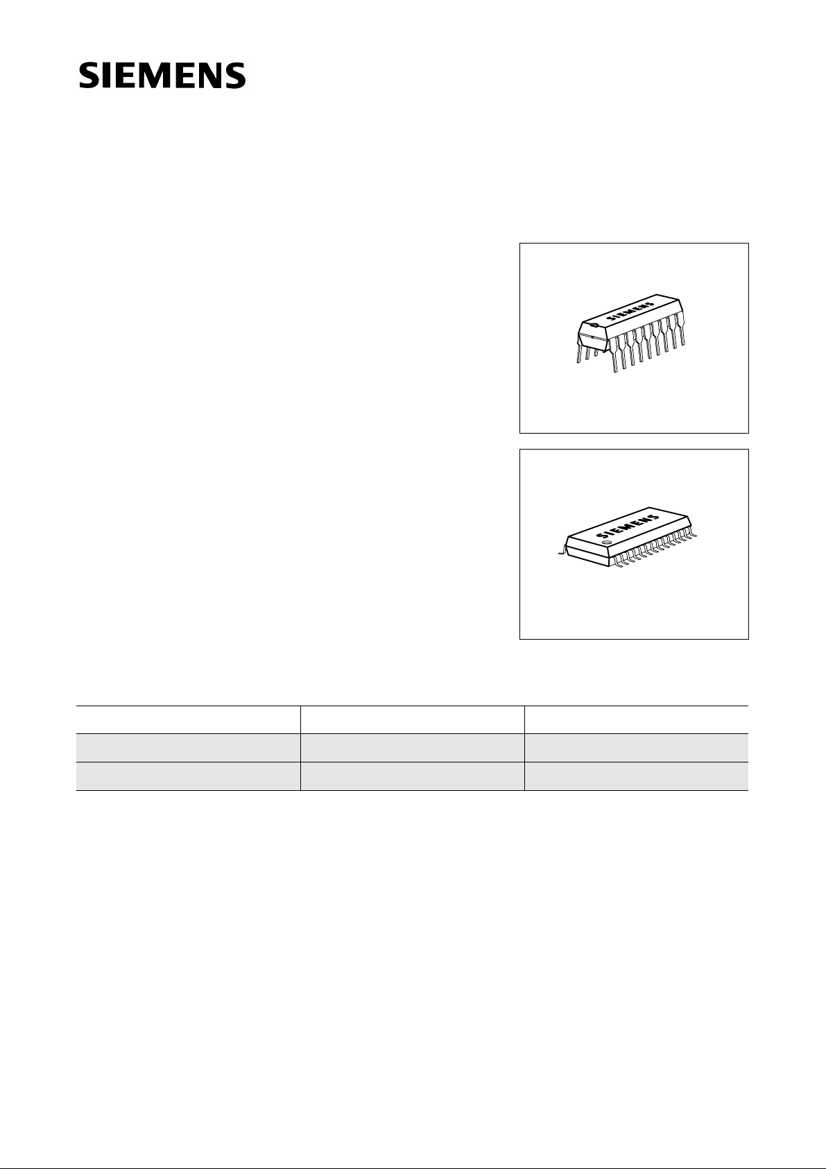
7 x 5 Video Matrix Switch TDA 6920
1 Overview
1.1 Features
● Fast I
● Cascadable (2 bus addresses)
● 7 CVBS inputs, 5 outputs
2
C Bus controlled (max. 400 kHz)
3 inputs with clamp disable by bus
● 1 input selectable as Y-input (S-VHS)
● 1 additional C-input (S-VHS)
● Y+C operation for S-VHS
P-DIP-18-5
selected by bus
● Fully ESD protected
● – 60 dB max. crosstalk at 5 MHz (P-DSO-28-1 only)
● Low operating voltage of 7.5 V
● 5 V operation is possible with reduced output signals
of max. 2 Vpp
● 15 MHz minimum bandwidth
● Noise insensitive clamping inputs
● Low impedance off condition
P-DSO-28-1
separate for each output
Type Ordering Code Package
TDA 6920 Q67000-A5200 P-DIP-18-5
TDA 6920X Q67007-A5225 GEG P-DSO-28-1
1.2 General Description
The TDA 6920 switches 7 video input sources to 5 outputs. Each output can be switched
to only one input, but one input can be switched to all outputs. The C-input may be
combined with one CVBS input as Y for Y+C (S-VHS) operation. Y+C operation is
selected by bus.
1.3 Application
● Television sets
● Satellite receivers
● Video mixing desks
Semiconductor Group 1 12.96
Page 2
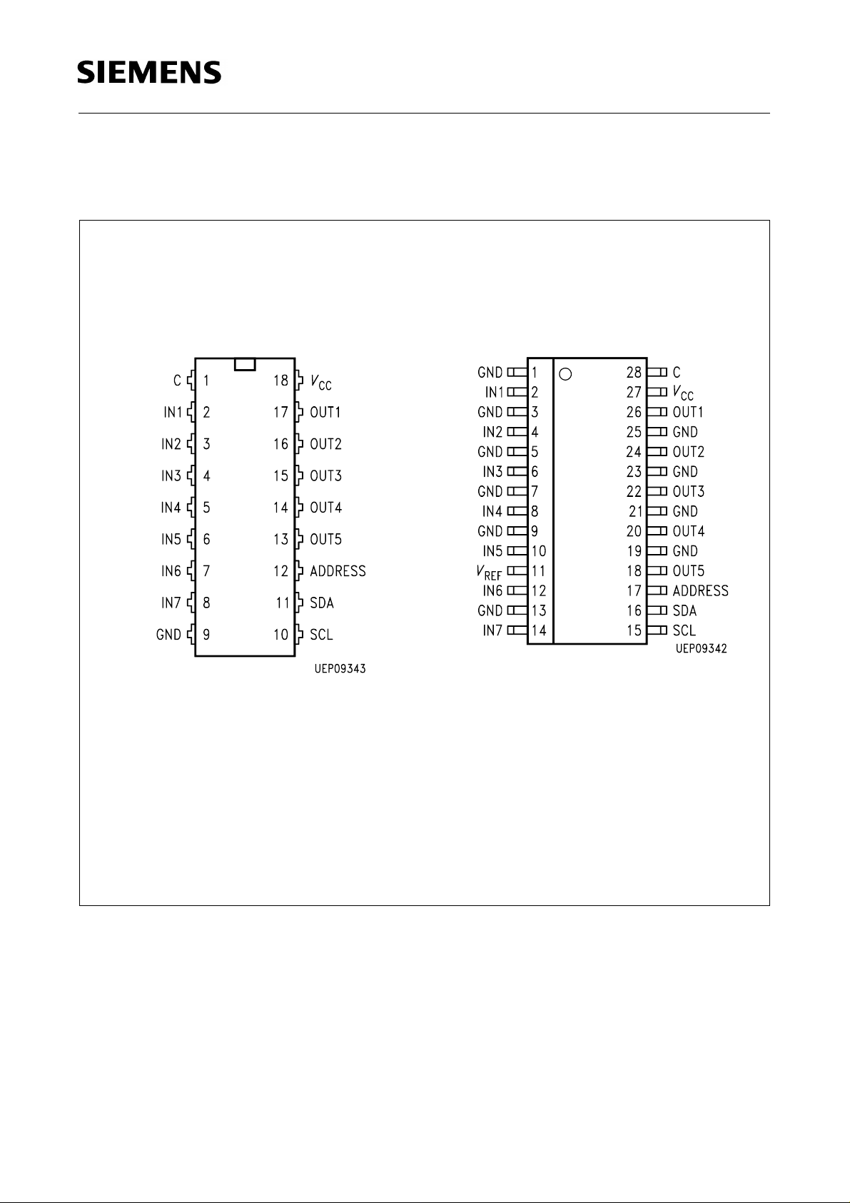
1.4 Pin Configuration
(top view)
P-DIP-18-5 P-DSO-28-1
TDA 6920
Figure 1
Semiconductor Group 2
Page 3
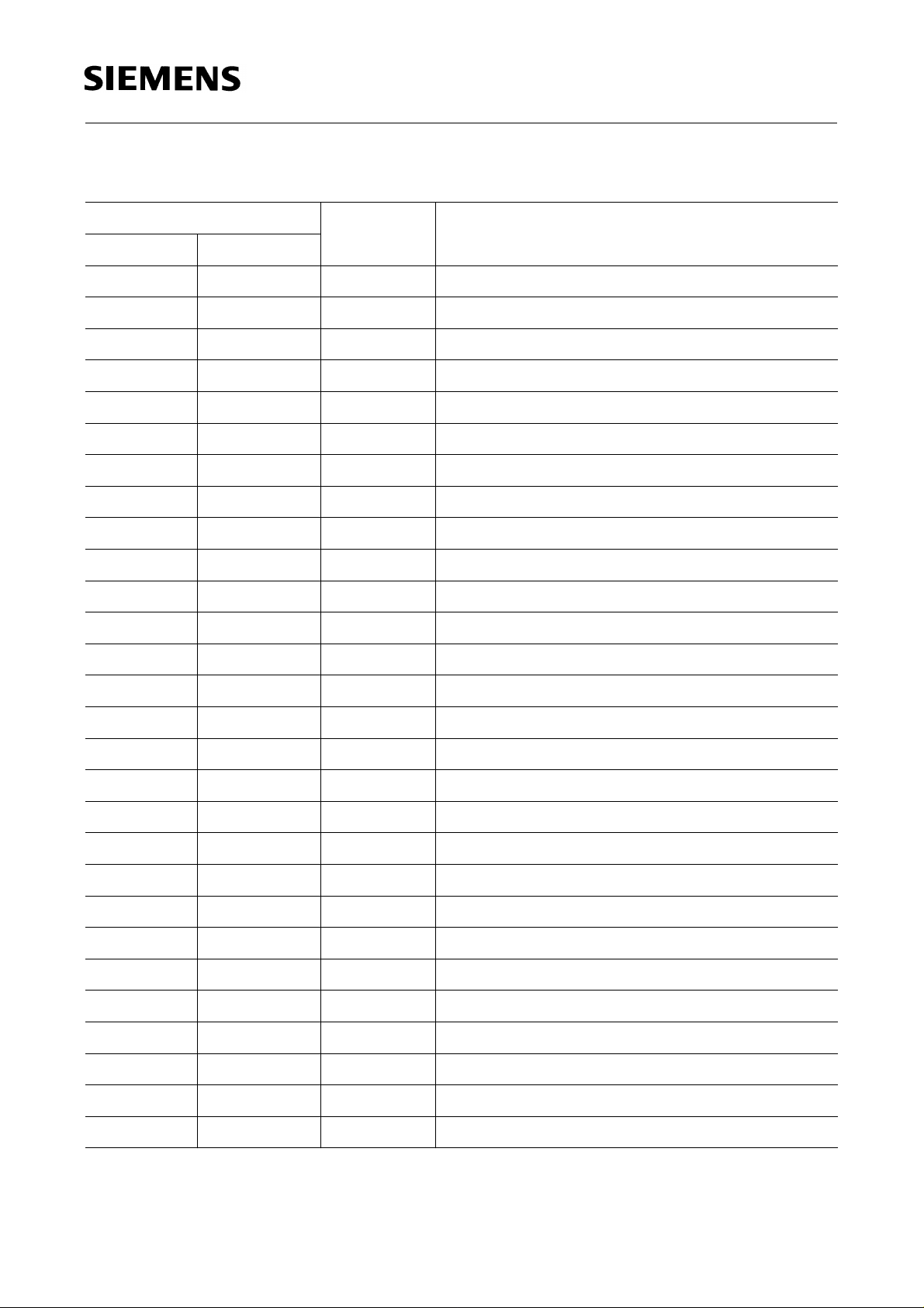
1.5 Pin Definitions and Functions
Pin No. Symbol Function
P-DIP-18-5 P-DSO-28-1
– 1 GND Signal and power supply ground
2 2 IN1 CVBS input 1
– 3 GND Signal and power supply ground
3 4 IN2 CVBS input 2
– 5 GND Signal and power supply ground
4 6 IN3 CVBS input 3
– 7 GND Signal and power supply ground
5 8 IN4 CVBS input 4
TDA 6920
– 9 GND Signal and power supply ground
6 10 IN5 CVBS input 5
–11
V
REF
Reference Voltage for external use
7 12 IN6 CVBS input 6
9 13 GND Power supply groung
8 14 IN7 CVBS input 7
10 15 SCL I
11 16 SDA I
2
C-Bus clock
2
C-Bus data
12 17 ADDRESS Address selection
13 18 OUT5 CVBS output 5
– 19 GND Signal and power supply ground
14 20 OUT4 CVBS output 4
– 21 GND Signal and power supply ground
15 22 OUT3 CVBS output 3
– 23 GND Signal and power supply ground
16 24 OUT2 CVBS output 2
– 25 GND Signal and power supply ground
17 26 OUT1 CVBS output 1
18 27
V
CC
Positive power supply voltage
1 28 C Separate color adding input for input 1
Semiconductor Group 3
Page 4
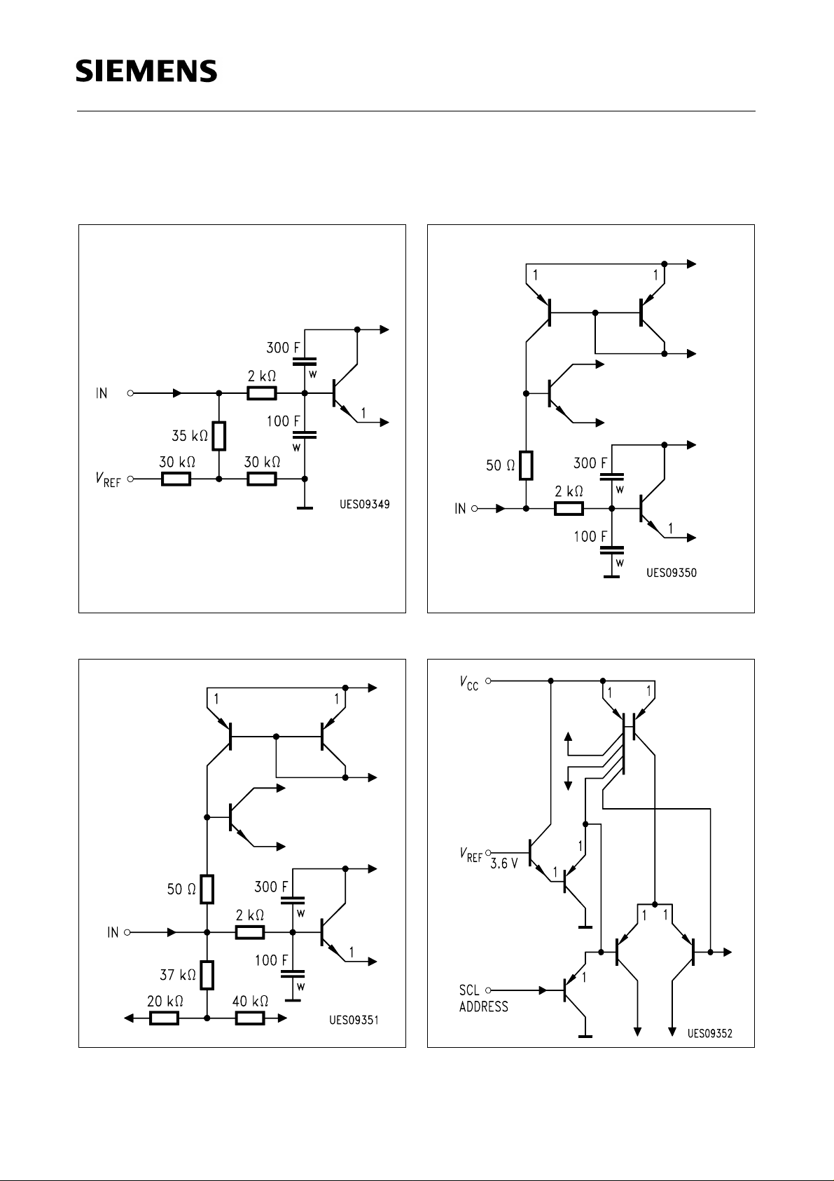
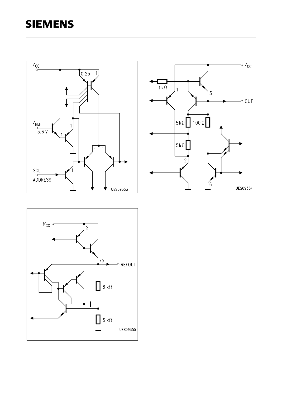
1.6 Pin Description
TDA 6920
Overview
C (color input)
In 2, 5, 6, 7 (CVBS input)
In 2, 3, 4 (CVBS input)
SCL, Address
Semiconductor Group 4
Page 5
TDA 6920
Overview
SDA
Out 1-5 (CVBS output)
V
(SO-28 only)
REF
Semiconductor Group 5
Page 6
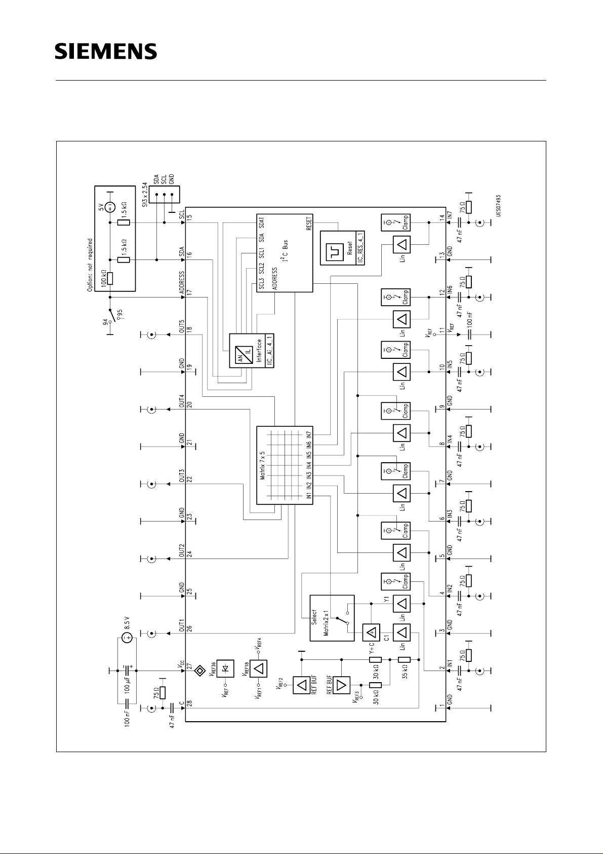
1.7 Functional Block Diagram
TDA 6920
Figure 2
Block Diagram (P-DSO-28-1)
Semiconductor Group 6
Page 7
TDA 6920
2 Functional Description
The main function of the IC is to switch 7 input video sources to 5 outputs.
Each output can be switched to only one input.
It is possible to have the same input connected to several outputs.
3 of the inputs can be used as non-clamping-input, switching is controlled by bus.
The clamping function of the other 4 inputs can be overriden by external resistor divider.
The other 4 inputs can be switched to non-clamping mode with external R/C network.
2
All switching possibilities are controlled by the I
All outputs can be switched to low impedance off condition by the I
Driving 75 Ω load requires external transistors for best performance.
The recommended coupling capacitor at each input is 47 nF.
Each clamping input requires a 75 Ω (max. 500 Ω) termination resistor.
C Bus.
2
C Bus.
Operation without or with a termination resistor greater than 500 Ω causes malfunction
of the new high performance clamping circuit.
Unused inputs should be directly grounded.
6 × 8 bits are necessary to determine one complete configuration change.
(1 addressbyte, 5 databytes)
Minimum configuration change for 1 output needs 2 × 8 bit (1 addressbyte, 1 databyte).
Power on reset state: all 5 outputs switched to input 1, all inputs clamped, Y+C off.
● Address Selection (fast I
2
C Bus)
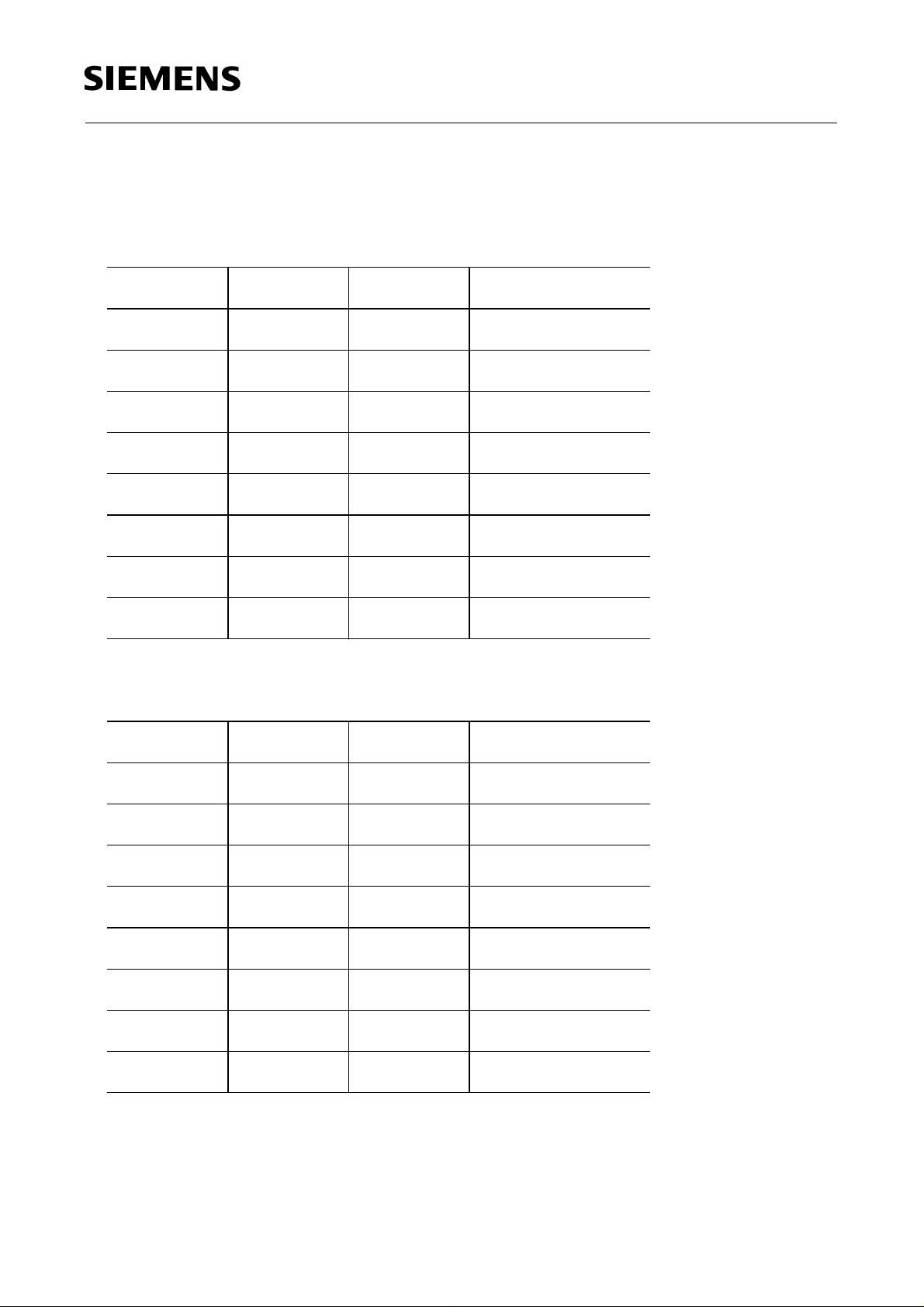
1st byte of transmisson (8 bit)
Hex Binary Address Pin
MSB LSB
96 1001 0110
V
(min. 3 V)
CC
94 1001 0100 GND
Semiconductor Group 7
Page 8
TDA 6920
● Data Mode Selections (fast I
2
C Bus)
2nd byte of transmission (8 bit)
Output Selection (3 bit, bit 7 must always be 0)
b7 b6
1)
b5 b4 b3 b2 b1 b0
1)
Selected Output
0X 000 XXX - not used
0X 001 XXX OUT1
0X 010 XXX OUT2
0X 011 XXX OUT3
0X 100 XXX OUT4
0X 101 XXX OUT5
0X 110 XXX - not used
0X 111 XXX - not used
1)
..X = don’t care
Input Selection Clamped (3 bit, bit 7 must always be 0)
b7 b6 b5 b4 b3
1)
b2 b1 b0 Selected Input
0X XXX 000 Output off condition
00 XXX 001 IN1
00 XXX 010 IN2
00 XXX 011 IN3
00 XXX 100 IN4
0X XXX 101 IN5
0X XXX 110 IN6
0X XXX 111 IN7
1)
..X = don’t care
Semiconductor Group 8
Page 9
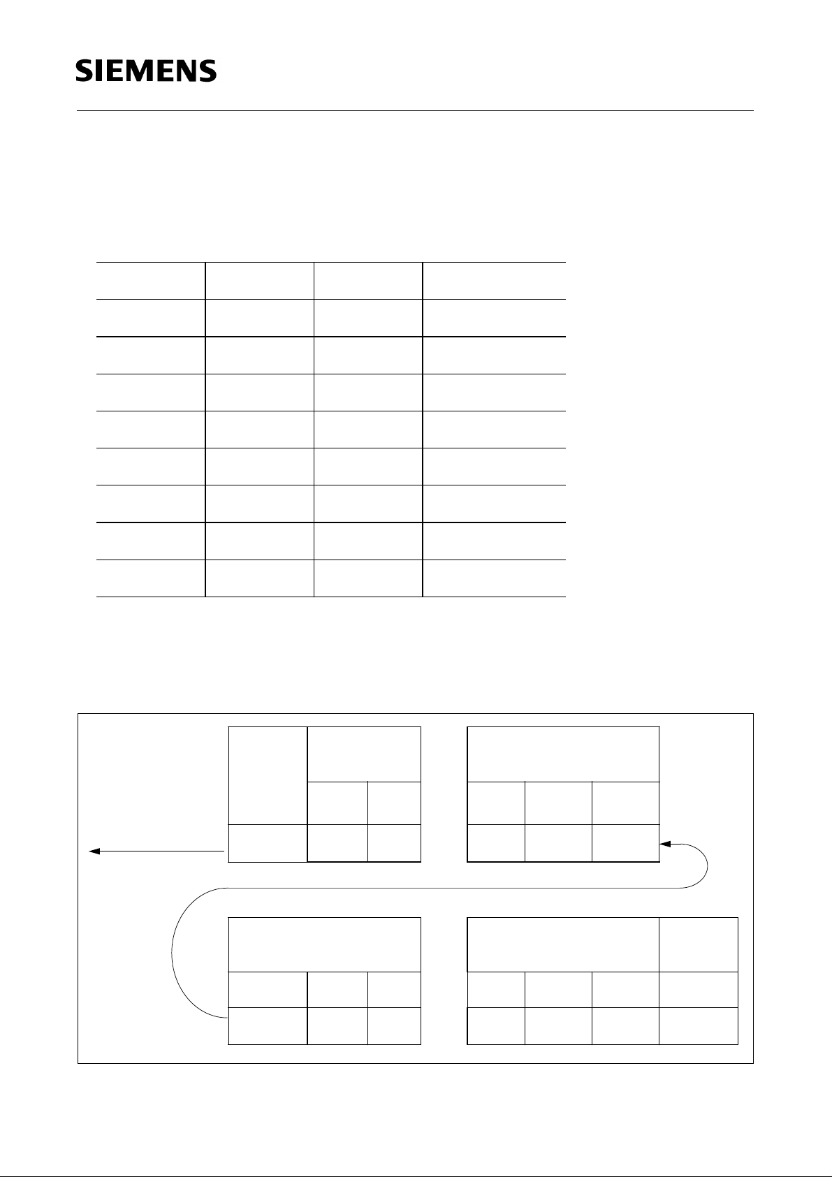
TDA 6920
● Data Mode Selections (fast I
2
C Bus) continued
2nd byte of transmission (8 bit)
Input Selection Non Clamped / Y+C (Y: always clamped. C: non clamped)
(3 bit, bit 7 must always be 0)
b7 b6 b5 b4 b3
1)
b2 b1 b0 Selected input
00 XXX 001 in1, (Y+C) off
00 XXX 010 in2, clamp on
00 XXX 011 in3, clamp on
00 XXX 100 in4, clamp on
01 XXX 001 in1, (Y+C) on
01 XXX 010 in2, clamp off
01 XXX 011 in3, clamp off
01 XXX 100 in4, clamp off
1)
X = don’t care (if only input operation mode change is requested, b5, b4
b3 should be 0, 0, 0: no output configuration is changed.)
● Bus Protocol (fast I
2
C Bus)
Programming Example: SDA sequence
serial data stream
address 96
start
condition
MSB LSB ..... mode output input
H
10 1001 0110 00 100 011
data: output 5 connect to
input 1 (Y+C)
1st data: output 4 connect
to input 3 clamped
last data: output 1 connect
to input 4 not clamped
stop
condition
..... mode output input ..... mode output input
01 101 001 01 001 100 01
Semiconductor Group 9
Page 10
TDA 6920
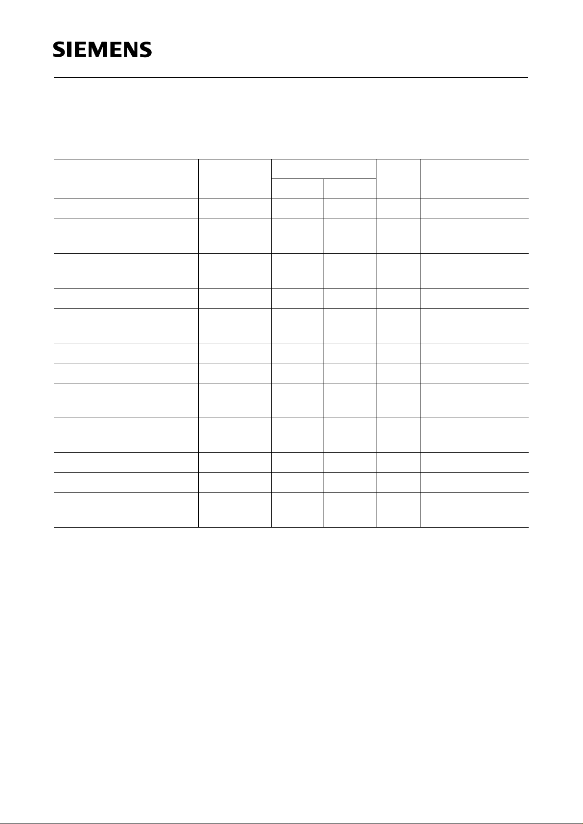
3 Electrical Characteristics
3.1 Absolute Maximum Ratings
Parameter Symbol Limit Values Unit Test Condition
min. max.
V
Supply voltage (
) V
CC
CC
014V
Reference voltage
(P-DSO-28-1 only)
Reference current
(
R
= 1 kΩ)
Lmin
Output voltage
Output current
(
R
= 500 Ω)
Lmin
Input voltage
Input voltage
SCL, SDA, address input
voltage
ESD-voltage all pins HBM
(
R = 1.5 kΩ, C = 100 pF)
Junction temperature
Storage temperature
Thermal resistance
(system - air)
V
REF
I
REF
V
OUT1 - OUT5
I
OUT1 - OUT5
V
C
V
IN1 - IN7
V
SDA, SCL,
Address
V
ESD
T
j
T
stg
R
th SA
05V
3.5 mA
0 V
CC
V
5mA
0 V
0 V
0 V
CC
CC
CC
V
V
V
– 6 6 kV
150 °C
– 40 125 °C
75 K/W
Note: Maximum ratings are absolute ratings; exceeding only one of these values may
cause irreversible damage to the integrated circuit.
Semiconductor Group 10
Page 11
TDA 6920
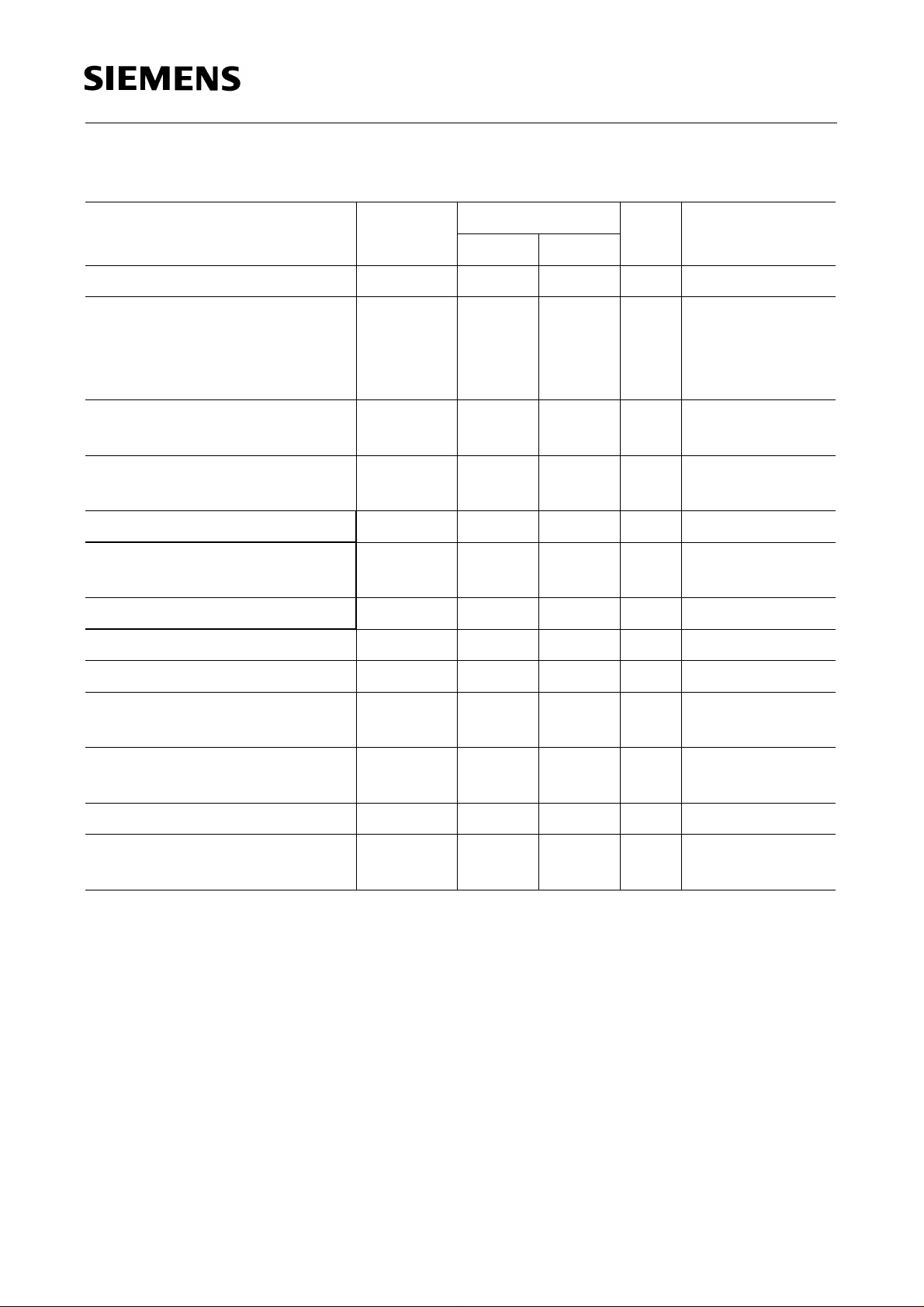
3.2 Operating Range
Parameter Symbol Limit Values Unit Test Condition
min. max.
Supply voltage
Absolute minimum supply
voltage (only usable with
reduced output signals of max.
2 Vpp)
Reference voltage
(P-DSO-28-1 only)
Video-input frequency range –
3dB
Video-input AC-voltage (color)
Video-input AC-voltage
(Y, CVBS)
Video-output AC-voltage
Input DC-voltage
Input DC-voltage (clamping)
Input DC-voltage
(non clamping)
V
CC
V
CC
V
REF
ƒ
IN IN1 - IN7, C
V
C
V
IN1 - IN7
V
OUT1 - OUT5
V
C
V
IN1 - IN7
V
IN2, 3, 4
7.5 13.2 V
4.5 V
3.3 3.9 V
0 20 MHz
1.0 Vpp
1.7 Vpp
3.4 Vpp
1.3 2.3 V
1.8 3.5 V
1.5 3.2 V
Input source-impedance
RI
IN1 - IN7
0 500 Ω
(clamping)
2
I
C-Bus clock ƒ
Ambient temperature during
IN SDA, SCL
T
A
0 500 kHz
– 10 85 °C
operation
Note: In the operating range the functions given in the circuit description are fulfilled.
Semiconductor Group 11
Page 12
TDA 6920
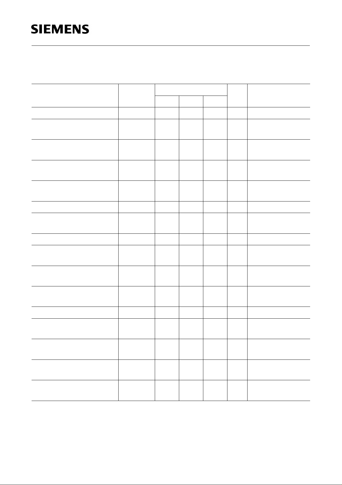
3.3 DC Characteristics
T
= 25 °C, VCC = 8.5 V
A
Parameter Symbol Limit Values Unit Test Condition
min. typ. max.
Total current consumption
Reference voltage
(P-DSO-28-1 only)
Output DC-voltage
(clamping)
Output DC-voltage
(output off)
Output current
Input DC-voltage
Input DC-voltage
(clamping)
Input current (clamping)
Input DC-voltage (for ext.
clamping override)
Input DC-voltage (non-
clamping, Bus controlled)
I
CC
V
REF
V
OUT1 - OUT5
V
OUT1 - OUT5
I
OUT1 - OUT5
V
C
V
IN1 - IN7
I
IN1 - IN7
V
IN1 - IN7
V
IN2, 3, 4
42 58 mA RL = ∝
3.4 3.6 3.8 V RL = ∝
1.8 V V
0.8 V V
0.5 1.0 2.0 mA V
C, IN1 - IN7
C, IN1 - IN7
= 2 V,
OUT
In = 0 Vpp
1.8 V VC = 0 Vpp
1.8 V V
0.33 1 µA I
2.4 V V
2.4 V V
IN1 - IN7
IN1 - IN7
IN1 - IN7
IN2, 3, 4
= 0 Vpp
= 0 Vpp
= 0 Vpp
= 0 Vpp
= 0 Vpp
= 0 Vpp
Input current
(SCL, SDA, address)
Output current (SDA)
Output voltage low (SDA)
SCL, SDA, address
(96 hex) : high
SCL, SDA, address
(94 hex) : low
SCL, SDA, address
(hysteresis)
I
SDA, SCL
I
Address
I
SDA
V
SDA
V
SDA
V
SDA, SCL
V
Address
V
SDA, SCL
V
Address
V
SDA, SCL
V
Address
0.1 0.4 µA V
6mAV
0
0
3.0 V
0.2
0.3
0.4
0.6
CC
V
V
V
SDA, SCL
V
Address
SDA
I
SDA
I
SDA
= 0 V
= 0 V
= 0.6 V
= 3 mA sink
= 3 mA sink
0 1.5 V
0.2 1 V dependant on
input frequency
Semiconductor Group 12
Page 13
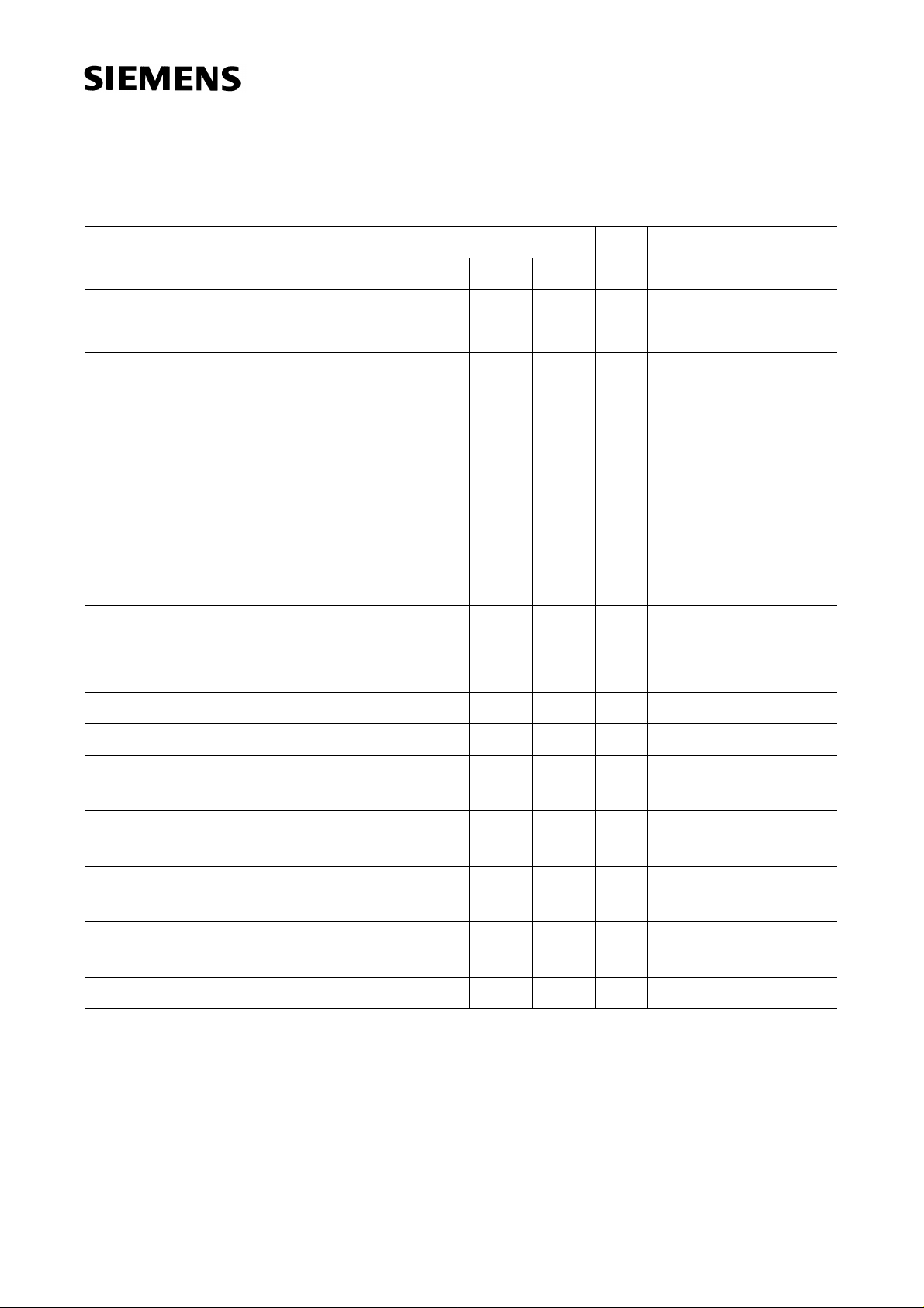
TDA 6920
3.4 AC Characteristics
T
= 25 °C, VCC = 8.5 V
A
Parameter Symbol Limit Values Unit Test Condition
min. typ. max.
Video bandwidth
Video gain
Crosstalk (0 - 5 MHz)
P-DSO-28-1
Crosstalk (0 - 5 MHz)
P-DSO-28-1
Crosstalk (0 - 5 MHz)
P-DIP-18-5
Crosstalk (0 - 5 MHz)
P-DIP-18-5
Input AC-voltage
Input AC-voltage
Input AC-voltage (sinus)
Output AC-voltage
2
I
C-Bus clock ƒ
P
OUT/IN
V
OUT/IN
A
A
A
A
V
C
V
IN1 - IN7
V
IN2, 3, 4
V
OUT1 - OUT5
IN SDA, SCL
15 20 MHz – 3 dB point
1.9 2.0 2.1
– 65 – 60 dB inputs 75 Ω to GND
– 55 – 50 dB inputs 500 Ω to GND
– 62 – 60 dB inputs 75 Ω to GND
– 45 – 50 dB inputs 500 Ω to GND
0.75 1 Vpp sinus
1 1.5 Vpp clamped
1 1.5 Vpp non clamped
2 3 Vpp
400 500 kHz
Output linearity
Input resistance
DG
OUT1-
OUT5
R
C, IN2, 3, 4
0.2 1 % RL = ∝
40 50 kΩ
(non-clamping)
Input source-impedance
R
IN1 - IN7
0 75 500 Ω
(clamping)
Input coupling-capacitor
(clamping)
Output dyn. impedance
C
IN1 - IN7
R
OUT1 - OUT5
47
nFµFCVBS-signal >
10
50 75 Ω
20 Hz Audiosignal
Note: The listed characteristics are ensured over the operating range of the integrated
circuit. Typical characteristics specify mean values expected over the production
spread. If not otherwise specified, typical characteristics apply at
T
=25°C and
A
the given supply voltage.
Semiconductor Group 13
Page 14
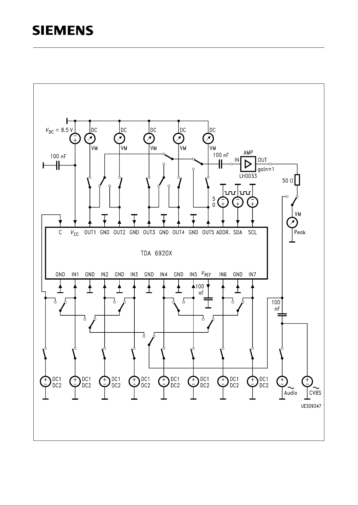
4 Test Circuits
TDA 6920
Figure 3
Test Circuit (P-DSO-28-1)
Semiconductor Group 14
Page 15
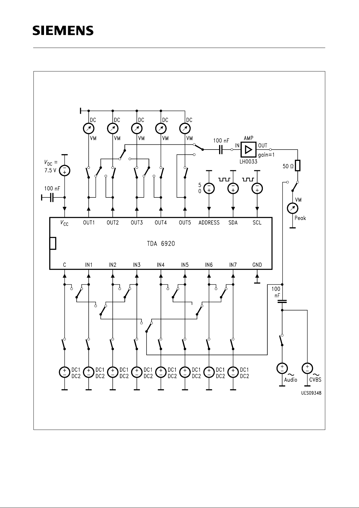
TDA 6920
Figure 4
Test Circuit (P-DIP-18-5)
Semiconductor Group 15
Page 16
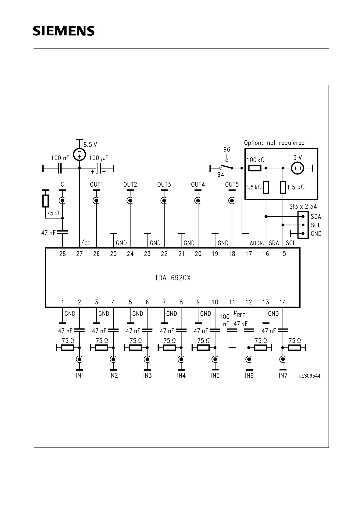
5 Application Circuits
TDA 6920
Figure 5
Application Circuit P-DSO-28-1 (clamping inputs)
Semiconductor Group 16
Page 17
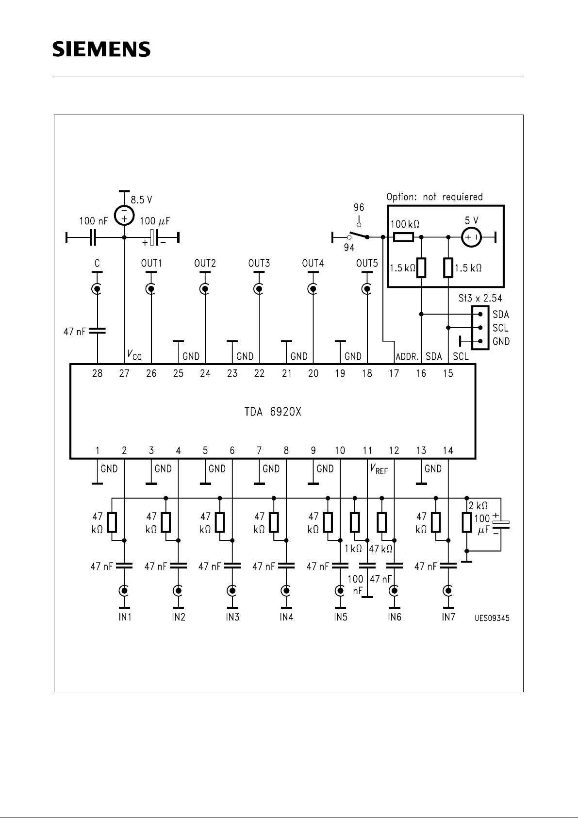
TDA 6920
Figure 6
Application Circuit P-DSO-28-1 (no clamping inputs with clamping overide)
Semiconductor Group 17
Page 18
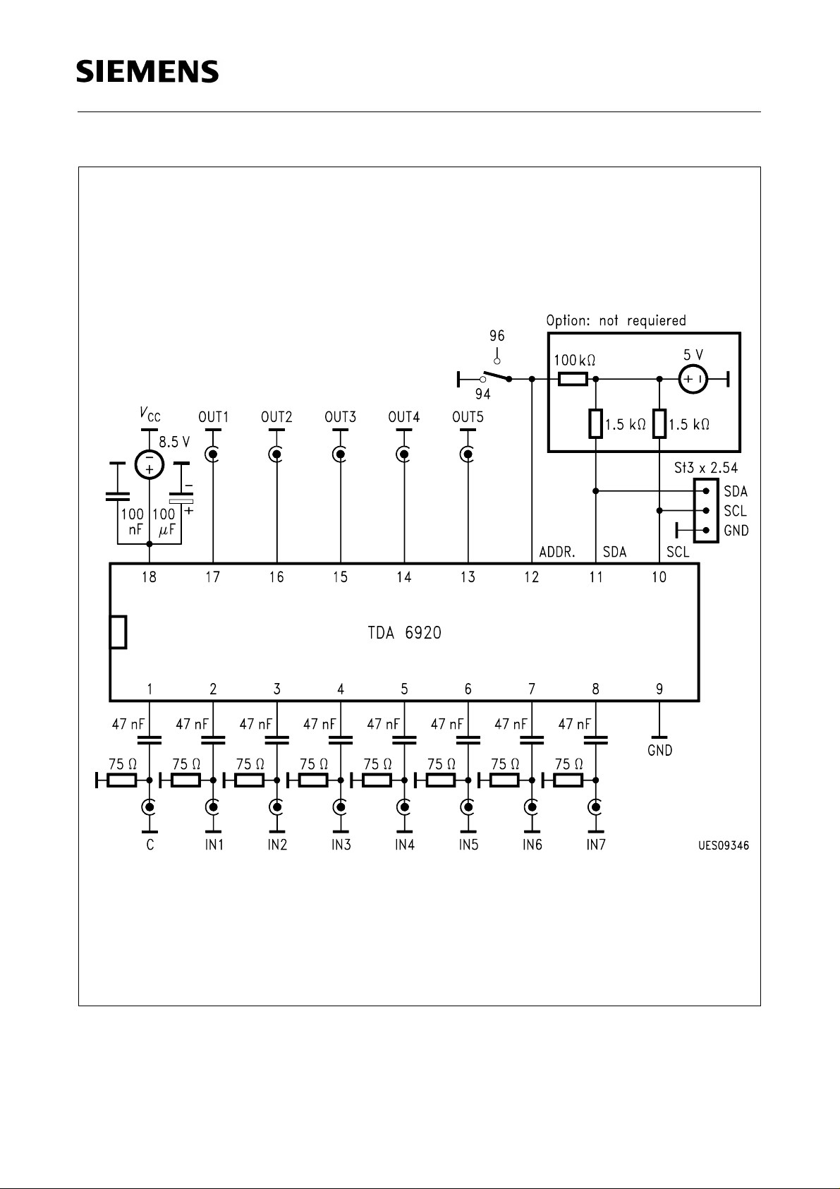
TDA 6920
Figure 7
Application Circuit (P-DIP-18-5)
Semiconductor Group 18
Page 19
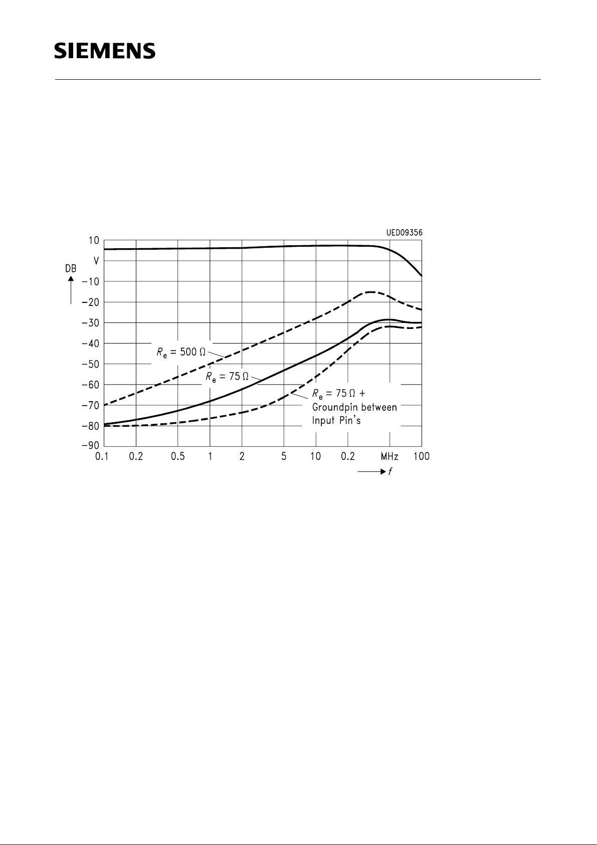
6 Electrical Diagrams
Typical frequency response and crosstalk
(simulated) for P-DSO-28-1 package
TDA 6920
V
Conditions:
= 8.5 V, all outputs selected to one different input;
CC
response: the measured output has max. signal on the selected input;
crosstalk: the measured output has no signal on the selected input, another input has
max. signal
Semiconductor Group 19
Page 20
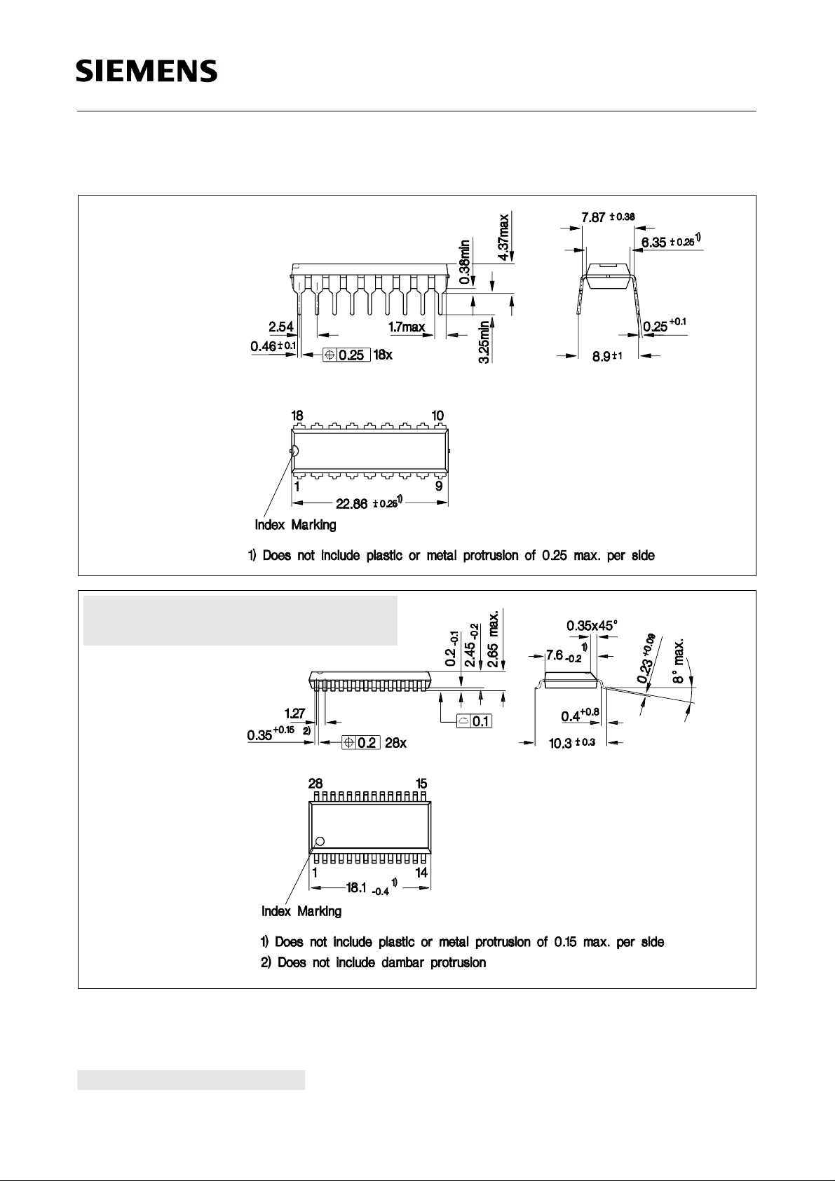
7 Package Outlines
P-DIP-18-5
(Plastic Dual in-line Package)
TDA 6920
P-DSO-28-1
(Plastic Dual Small Outline Package)
GPD05586
Sorts of Packing
Package outlines for tubes, trays etc. are contained in our
Data Book “Package Information”.
SMD = Surface Mounted Device
Semiconductor Group 20
GPS05123
Dimensions in mm
 Loading...