

Page 1
Multistandard Sound IF
TDA 6160-2X
Preliminary Data Bipolar IC
Features
● Sound carrier mixer
● VCO
● Programmable Divider
● Reference divider with crystal oscillator
● Phase comparator
● Operational amplifier for PLL filter
2
● I
C bus interface
● 3 identical FM channels with limiter amplifiers
P-DSO-28-1
and coincidence demodulators.
Type Ordering Code Package
TDA 6160-2X Q67000-A5085 P-DSO-28-1 (SMD)
Functional Description
Multistandard sound IF-device consisting of a mixer as a frequency converter, a voltage-controlled
oscillator (VCO) that can be continuously tuned in 10-kHz increments with crystal accuracy by
means of a PLL, and three following parallel FM-limiter amplifiers with coincidence demodulators.
The switching functions and setting of the PLL are controlled on an I2C bus.
Application
For use in satellite receivers.
Semiconductor Group 143 08.93
Page 2
Pin Functions
Pin No. Function
1 Quartz oscillator
TDA 6160-2X
2 PD-output / integrator input (
V
3 Integrator output (
)
D
4 VCO
5 Chip address switching (CA)
6 Demodulator circuit (IF-1)
7 Demodulator circuit (IF-1)
8 AF-output 1
9 Demodulator circuit (IF-2)
10 Demodulator circuit (IF-2)
11 AF-output 2
12 Demodulator circuit (IF-3)
13 Demodulator circuit (IF-3)
14 AF-output 3
15 IF-input 3
16
V
(analog)
S
17 IF-input 2
f
REF
, fCy)
18 Ground (analog)
19 IF-input 1
20 IF-reference
21 Mixer output 2
22 Mixer output 1
23 Mixer input (reference)
24 Mixer input
25 Ground (digital)
26
27 I
28 I
V
(digital)
S
2
C bus (SCL)
2
C bus (SDA)
Semiconductor Group 144
Page 3
Pin Functions
TDA 6160-2X
Pin 1
Pin 2/3
Semiconductor Group 145
Page 4
TDA 6160-2X
Pin 4
Pin 6/7/8; 9/10/11; 12/13/14
Semiconductor Group 146
Page 5
TDA 6160-2X
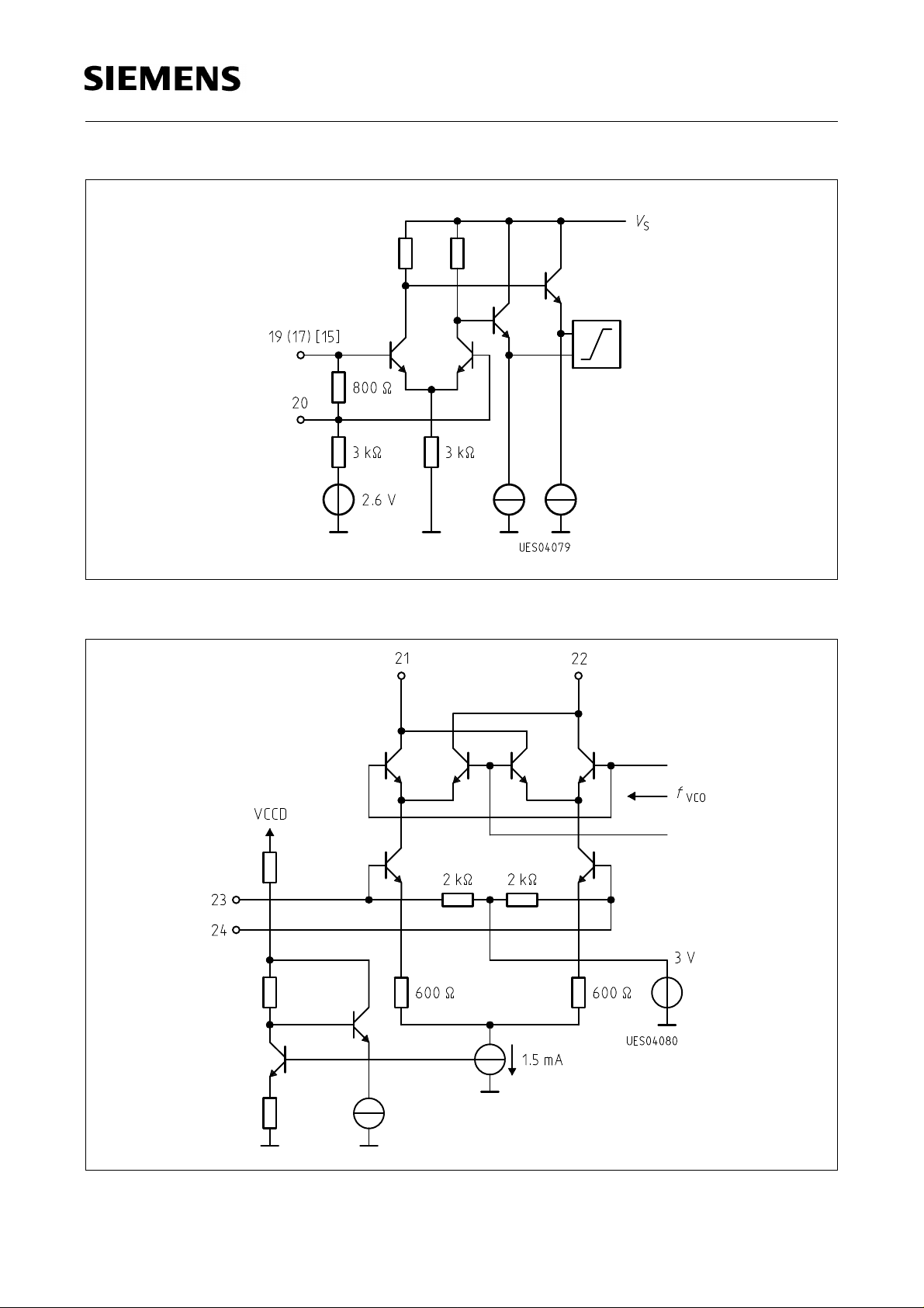
Pin 19; 17; 15/20
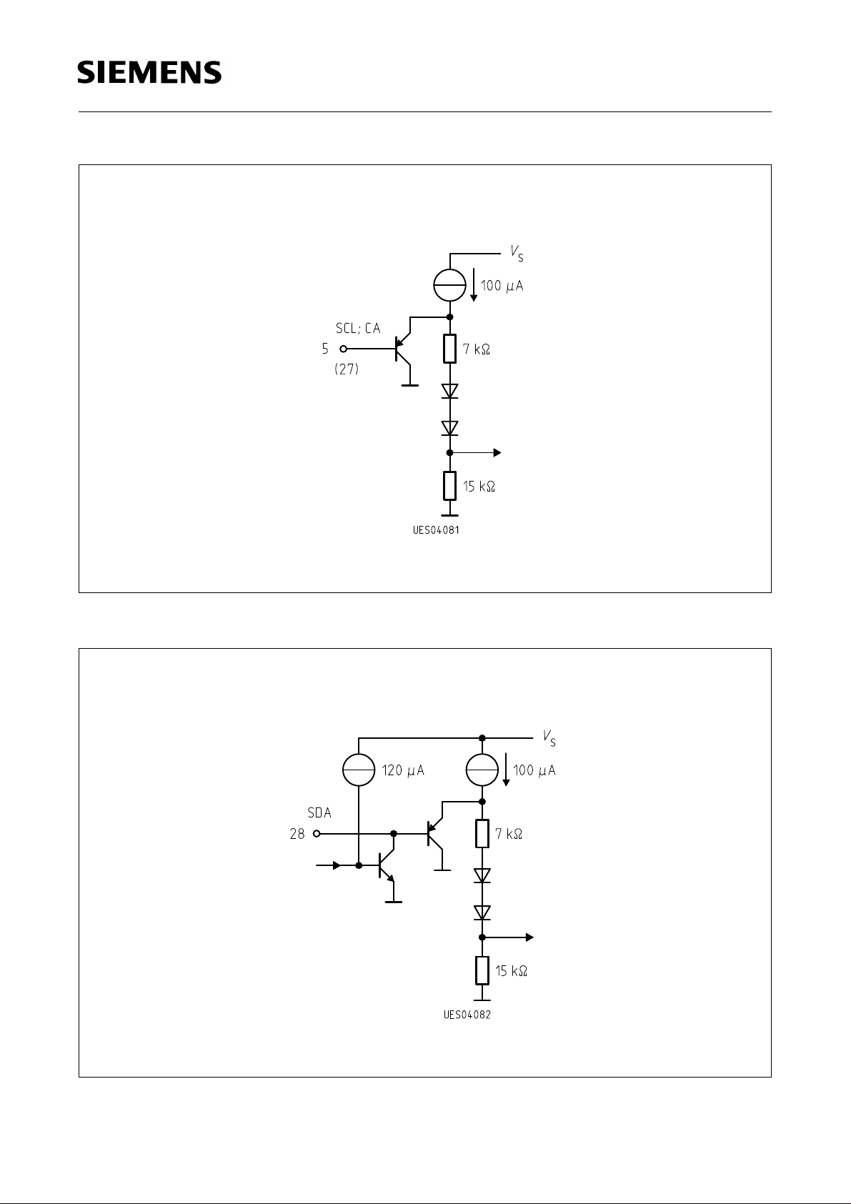
Pin 21/22/23/24
Semiconductor Group 147
Page 6
TDA 6160-2X
Pin 5; 27
Pin 28
Semiconductor Group 148
Page 7

TDA 6160-2X
Block Diagram
Semiconductor Group 149
Page 8

TDA 6160-2X
Circuit Description
The sound intermediate frequencies contained in the baseband of a demodulated FM satellite
signal can lie between 5 and 9 MHz. This band of frequencies is applied ready filtered to the input
of the converter mixer. The purpose of this mixer is to convert the different sound IFs in the
baseband to fixed output frequencies (e.g. 10.7/10.52 MHz). These frequencies are then fed by
external filters to the inputs of the three sound IF-amplifiers.
The VCO of the mixer can be continuously tuned between 14.5 and 20 MHz in 10-kHz increments
with crystal accuracy by means of a PLL-circuit.
The setting of the programmable divider and the cutting in and out of the sound IF-amplifiers are
controlled on the I2C bus.
Pin 5 (CA) offers two switchable chip addresses to enable parallel operation of two devices.
All pins are guarded against electrostatic discharge. SCL and SDA include special protective
structures to permit continued bus operation when the device is switched off.
PLL
The VCO-signal, DC coupled internally, is applied to the PLL-input. It passes through a
programmable divider (N = 1024 to 2047) and is then compared to a reference frequency
(f
= 10 kHz) in a digital frequency/phase detector. This frequency is derived from a 4-MHz crystal
REF
oscillator whose signal is divided by 400.
The phase detector has a charge-pump push-pull current output. If the negative edge of the divided
VCO-signal appears before the negative edge of the reference signal, the current source I+ will
pulse for the duration of the phase difference. In the reverse case it is the current sink I–. If both
signals are in-phase, the output is high-impedance and the PLL is locked in. The current pulses are
filtered by means of an integrator (internal operational amplifier with external RC-circuitry).
The pump current can be switched between the two values 1 and 5 by software with a control bit 5I.
This permits a change in the control response during and after the lock-in state.
I2C Bus Interface
Information is exchanged between the processor and the sound IF-device on an asynchronous
bidirectional data bus. The timing for this comes from the processor (input SCL), while pin SDAfunctions as an input or output depending on the direction of the data (open collector; external
pull-up resistor).
The data from the processor go to an I2C bus controller and are filed in registers (latches 0 to 2)
according to their function. When the bus is not busy, both lines are in marking state (SDA, SCL are
high). Each telegram begins with the start condition: SDA goes low while SCL remains high. All
further exchanges of information are while SCL is low and are read by the controller with the positive
clock edge. If SDA goes high while the clock is high, the PLL recognizes this as a stop condition and
thus the end of the telegram.
For what follows, refer to the table of logic assignments below.
All telegrams are transferred byte by byte, followed by a ninth clock pulse during which the controller
pulls the SDA-line to low (i.e. acknowledge condition). The first byte consists of seven address bits
with which the processor selects the PLL from among several peripheral devices (chip select). The
Semiconductor Group 150
Page 9

TDA 6160-2X
eighth bit is always low. The first bit of the first or third data byte in the data part of the telegram
determines whether a divider ratio or control information will follow. In every case the first byte must
be followed by a byte of the same data type (or a stop condition). When the supply voltage is
applied, a power-on reset circuit prevents the PLL from pulling the SDA-line to low and thus blocking
the bus.
Logic Allocations
Address byte
Progr. divider byte 1
Progr. divider byte 2
Control information
Address byte 1
Address byte 2 = H46
01000MA1MA0R/WA
0 0 n10 n9 n8 n7 n6 n5 A
n4 n3 n2 n1 n0 0 0 0 A
1 5IZ2Z1Z0T2T1T0 A
01000100A
= H44
01000110A
Chip address (CA)
pin 5 on: ground = address byte 1
V
or open = address byte 2
S
Test Mode
T2, T1, T0 = 0, 0, 0 normal operation
T2, T1, T0 = 1, 0, 0 pin 2 = f
T2, T1, T0 = 1, 1, 0 pin 2 = f
REF
Cy
T2, T1, T0 = 1, 1, 1 pin 2 = tristate
T2, T1, T0 = 0, 1, 1 pin 2 = high-impedance = pin 3 high-impedance
IF-Muting Circuits
Z2, Z1, Z0 = 0, 0, 0 normal operation
Z2, Z1, Z0 = 0, 0, 1 IF 3 = off (output 14 high-impedance)
Z2, Z1, Z0 = 0, 1, 0 IF 2 = off (output 11 high-impedance)
Z2, Z1, Z0 = 0, 1, 1 IF 1 = on; IF 2/IF 3 = off
Z2, Z1, Z0 = 1, 0, 0 IF 1 = off (output 8 high-impedance)
Z2, Z1, Z0 = 1, 0, 1 IF 1 = off; IF 2 = on; IF 3 = off
Z2, Z1, Z0 = 1, 1, 0 IF 3 = on; IF 1/IF 2 = off
Z2, Z1, Z0 = 1, 1, 1 IF 1, IF 2, IF 3 = off
Semiconductor Group 151
Page 10

TDA 6160-2X
Telegram Examples
Start-AB-DB1-DB2-CI-Stop Start = start condition
AB = address byte
Start-AB-CI-DB1-DB2-Stop DB1 = divider byte 1
Start-AB-DB1-Stop DB2 = divider byte 2
CI = control information
Start-AB-CI-Stop Stop = stop condition
Converter Mixer + VCO
In the converter mixer the sound subcarriers (frequency band approx. 5 to 9 MHz) contained in the
baseband of the received composite signal are converted to an output frequency of 10.52 MHz or
10.7 MHz for example. The two mixer outputs are designed as open-collector outputs.
The VCO has internal feedback and its frequency of 15.5 to 19.7 MHz is determined by an external
resonant circuit with a varactor diode that is tuned by the PLL. The resonant circuit is connected to
the supply voltage by its low side.
IF-Limiter with Demodulators
The limiter amplifiers are implemented as balanced five-stage, capacitively coupled differential
amplifiers. All there limiter inputs have a common reference (pin 20).
The output signals of the limiter amplifiers are fed direct and via an external phase-shifter circuit to
the coincidence demodulators. The AF-signals can be brought out an disconnectible (by Z2, Z1, Z0)
AF output stages. The outputs are high-impedance when they are disconnected.
Semiconductor Group 152
Page 11

TDA 6160-2X
Absolute Maximum Ratings
T
= 0 to 70 °C
A
Parameter Symbol Limit Values Unit
min. max.
Supply voltage V16, V
I
AF-output
AF-output
Demodulators
IF-inputs
Mixer outputs
VCO
Crystal oscillator
Junction temperature
Storage temperature
Thermal resistance
, I11, I
8
V
, V11, V
8
V
6/7
V
15
V
21
V
4
V
1
T
j
T
stg
R
th SA
, V
, V17, V
, V
26
9/10
22
14
14
, V
12/13
19
06V
– 1.5 3 mA
0 V
0 V
V
16
16
16
V
V
V
7V
7V
0 1.5 V
150 °C
0 125 °C
90 K/W
All voltage values are referred to ground (pin 18, pin 25), unless stated otherwise.
All currents are designated according to the source and sink principle, i.e. if the device pin is to be
regarded as a sink (the current flows into the stated pin to internal ground), it has a negative sign,
V
and if it is a source (the current flows from
across the designated pin), it has a positive sign.
S
Operating Range
Supply voltage
Input frequency range
of converter mixer
Input frequency range of sound
IF-amplifiers (– 3 dB)
VCO-frequency
Ambient temperature
V
, V
16
f
I24
f
I15, 17, 19
f
O4
T
A
26
4.5 5.5 V
5 9 MHz
5 15 MHz
5 20 MHz
070°C
Semiconductor Group 153
Page 12

TDA 6160-2X
Characteristics
V
= 5 V; TA = 25 °C
S
Parameter Symbol Limit Values Unit Test Condition
min. typ. max.
Current drain (analog section) I
Current drain (digital section)
16
I
26
Phase-detector
charge current
I
PD
Mixer
Static Characteristics
Mixer output currents
I
21, 22
Output-current difference I21 – I
Mixer inputs V
23, 24
Dynamic Characteristics
Input voltage for IMA > 60 dB
Input-frequency band f
Input-resistance
Output-frequency band
Frequency band of VCO ∆
Mixer gain
V
24
I24
R
23/24
f
O21/22
f
G
Mi
4
Output-voltage range
on mixer
33 42 mA
20 35 44 mA
± 32
± 160
± 40
± 250
± 75
± 360µAµA
1.1 3.5 mA V23 = V
22
100 µA V23 = V
3V
180 230 mVrms SC1 = 6 MHz;
5 9 MHz
4kΩ
11 MHz
15 20 MHz
– 8– 4– 2dB R
V
16
– 0.4
V
16
max
V IMA > 55 dB;
I
5I
24
24
SC2 = 6.5 MHz;
SC3 = 7 MHz;
V
= V
SC1
= 470 Ω
L
V
<180mVrms
23/24
SC2
= V
SC3
Semiconductor Group 154
Page 13

TDA 6160-2X
Characteristics (cont’d)
Parameter Symbol Limit Values Unit Test Condition
min. typ. max.
Sound IF (for all three amplifiers)
Static and Dynamic Characteristics
Input-frequency band f
Input voltage to
activate limiting
(
V
– 3 dB) V
qAF
AF-output voltage
Distortion factor
AM-rejection
AM-rejection
15, 17, 19
15, 17, 19
V
8, 11, 14
THD
a
AM
a
AM
8, 11, 14
5 15 MHz
70 250 µV
150 220 300 mV f
0.2 % f
45 dB V
25 dB V
f
I15, 17, 19
= 10.7 MHz;
∆f = 30 kHz;
f
= 1 kHz
mod
I15, 17, 19
= 10.7 MHz;
∆f = 30 kHz;
V
I15, 17, 19
f
mod
I15, 17, 19
=10 mV,
= 1 kHz
= 10.7 MHz;
∆f = 30 kHz;
V
I15, 17, 19
f
mod
I15, 17, 19
=10 mV,
= 1 kHz
=20 to
100 mV; m = 30%
= 2 mV;
I15
m = 30%
AF-output DC-voltage 2.2 V
Design Notes
Sound IF-input resistance
Demodulator input resistance
AF-output resistance
Residual IF-voltage
R
15/20
R
17/20
R
19/20
R
6/7
R
9/10
R
12/13
R
8, 11, 14
V
IF8, 11, 14
800 Ω
30 kΩ
100 Ω
5mV
Hum suppression
(without deemphasis)
a
H
25 dB VS = 5 V;
Semiconductor Group 155
V
= 250 mVpp;
H
f
= 50 Hz
H
Page 14

TDA 6160-2X
Characteristics (cont’d)
Parameter Symbol Limit Values Unit Test Condition
min. typ. max.
I2C Bus (SCL, SDA)
Edges SCL, SDA
Rise time
Fall time
Shift clock SCL
Frequency
H-pulse width
L-pulse width
Start
Setup time
Hold time
Stop
Setup time
Bus free
Data change
Setup time
Hold time
Inputs SCL, SDA
Input voltage
t
R
t
F
f
SCL
t
H
t
L
t
SUSTA
t
HDSTA
t
SUSTO
t
BUF
t
SUDAT
t
HDDAT
V
IH
V
IL
1
300
0
100 kHz
4
4
4
4
4
4
1
1
2.4 5.5
1
µs
ns
µs
µs
µs
µs
µs
µs
µs
µs
V
V
Input current
Output SDA (open collector)
Output voltage
Address byte 1 = L
Address byte 2 = H or open
I
IH
I
IL
V
QH
V
QL
V
5L
V
5H
4.5 5.5
01V
2.4 5.5 V
Semiconductor Group 156
10
10
0.4
µA
µA
V
V
R
= 2.5 kΩ
L
I
= 3 mA
QL
Page 15

TDA 6160-2X
Test Circuit
Semiconductor Group 157
Page 16

TDA 6160-2X
Application Circuit
Semiconductor Group 158
Page 17

TDA 6160-2X
I2C Bus Timing Diagram
t
SUSTA
t
HDSTA
t
H
t
L
t
SUDAT
t
HDDAT
t
SUSTO
t
BUF
t
F
t
R
Setup time (start)
Hold time (start)
H-pulse width (clock)
L-pulse width (clock)
Setup time (data change)
Hold time (data change)
Setup time (stop)
Bus free time
Fall time
Rise time
All times referred to VIH and VIL values
Semiconductor Group 159
 Loading...