

Page 1
Video IF with FPLL,
MAC State
Features
● Active multistandard video IF
with FPLL demodulator
● 12-MHz bandwidth
● MAC state
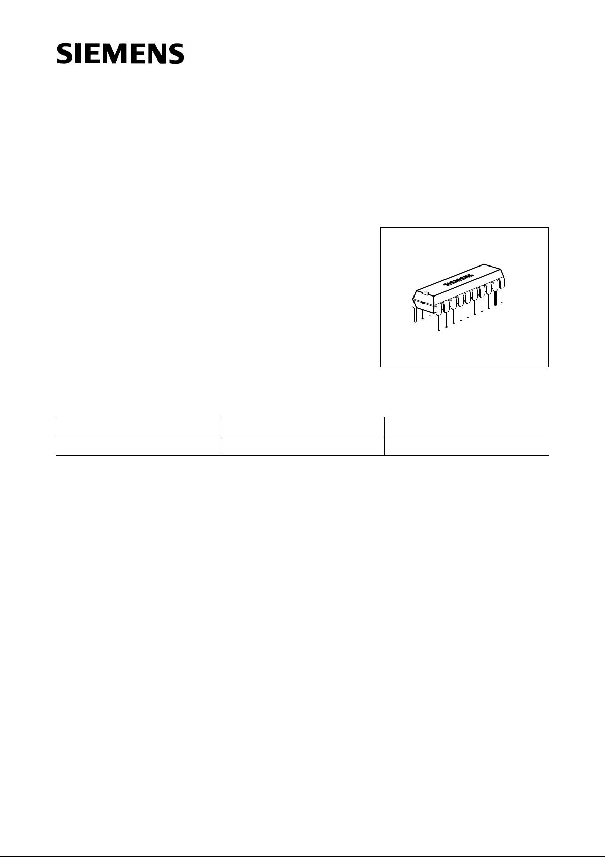
TDA 6050-5
Bipolar IC
P-DIP-20
Type Ordering Code Package
TDA 6050-5 Q67000-A5123 P-DIP-20
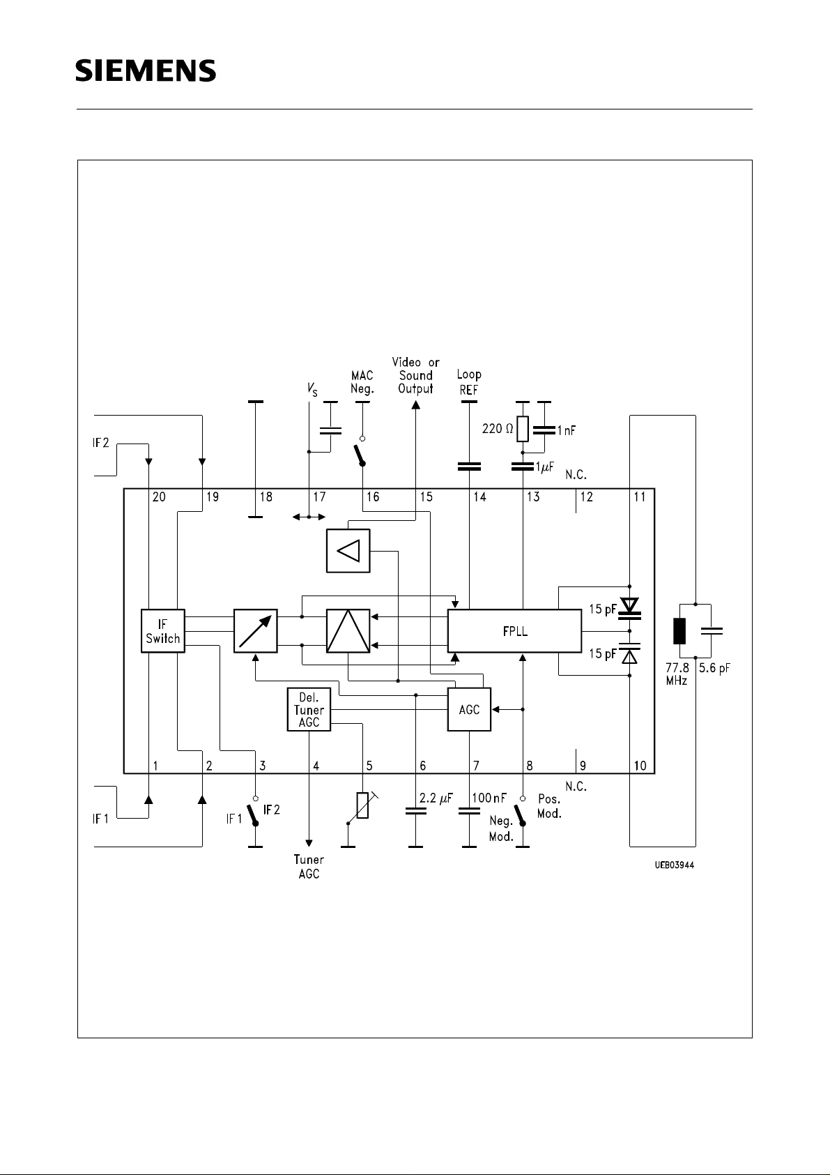
Circuit Description
The IF circuit consists of a four-stage capacitively coupled and symmetrically designed controlled
amplifier and a real synchronous demodulator with a FPLL-carrier regeneration. Two IF inputs can
be selected for applications with different SAWs. The main performance of the device is the very low
differential phase DP and gain DG combined with an excellent intermodulation ratio. The positive
video output is used to derive the IF and tuner control voltage. The AGC threshold is set by means
of a potentiometer. Dependent on the modulation polarity the video signal and the AGC are
switched over. MAC state can be selected by an additional signal.
Application
Multistandard TV/VTR and cable converters with mono or stereo applications.
Semiconductor Group 63 06.94
Page 2
Pin Functions
Pin No. Function
1 IF input 1a
2 IF input 1b
3 IF switch
4 Tuner AGC output
5 Tuner AGC threshold
6 Main AGC-time constant
7 Mean value AGC-time constant
8 Positive/negative modulation switch
9 N.C.
10 FPLL-VCO (2 × video carrier)
TDA 6050-5
11 FPLL-VCO (2 × video carrier)
12 N.C.
13 FPLL-loop filter
14 FPLL-loop reference
15 Video output
16 MAC-standard switch
17 +
18 Ground
19 IF input 2a
20 IF input 2b
V
supply voltage
S
Semiconductor Group 64
Page 3
TDA 6050-5
Block Diagram
Semiconductor Group 65
Page 4

TDA 6050-5
Absolute Maximum Ratings
T
= 0 to 70 ˚C
A
Parameter Symbol Limit Values Unit
min. max.
Supply voltage V
Junction temperature
Storage temperature
Thermal resistance
(system-air)
Operating Range
Supply voltage V
Supply voltage delayed tuner AGC
IF-frequency range
Ambient temperature during operation
T
T
R
V
f
IF
T
17
j
stg
th SA
17
5
A
0 13.2 V
150 ˚C
– 40 125 ˚C
60 K/W
10.8 13.2 V
0.8 12 V
12 80 MHz
– 10 85 ˚C
Semiconductor Group 66
Page 5

DC Characteristics
T
= 0 to 85 ˚C; VS = 12 V
A
Parameter Symbol Limit Values Unit Test Condition
min. typ. max.
TDA 6050-5
Total current
consumption
IF input
IF switch
H or open = IF 1
L = IF 2
Standard switch
H level
L level
B/G standard
L standard
MAC standard
AGC Voltage
Min. AGC
Max. AGC
– I
V
V
±
V
V
±
± I
V
V
V
V
17
, V2,
1
19
I
3
3
3
I
8
16
, V
8
, V
8
6
6
, V
51 mA
5.7 6.0 6.3 V
20
120
210 260
2.0
0.0
16
16
120
2
0
210 260
0.0 0.1
2.8
5.0
1.0
5
1
0.5
4.0
µA
V
V
µA
V
V
V
V
V
= 0 V, 5 V
3
V
, V16 = 0 V, 5 V
8
V
= H V16 = H
8
V
= L V16 = H
8
V
= H V16 = L
8
V
, V
1-2
19-20
V
, V
1-2
19-20
= 0 Vrms
= 150 mVrms
AGC-Time Constant with Neg. Modulation
Charge current
Discharge current
Charge/discharge
I
6
– I
∆I
1.1
6
6
13
55
1.4
18
82
ratio
AGC-Time Constant with Pos. Modulation
Charge current
Discharge current
Discharge current
I
6
– I
– I
1.1
6
6
0.15
70
1.4
0.25
85
(Average control)
Charge/discharge
∆I
6
4000
5600
ratio
Mean Value Generation with Pos. Modulation
White level
Zero carrier level
V
7
V
7
4.9
3.3
5.7
3.7
1.9
23
140
1.9
0.35
120
9000
6.5
4.1
mA
µA
mA
µA
µA
V
V
V
= 2.0 V, V15≤ 3.2 V
6
V
= 2.0 V, V15≥ 4.2 V
6
V
= 2.0 V, V15 ≥ 7.0 V
6
V
= 2.0 V, 5.2 V < V15 < 6.5 V
6
V
= 2.0 V, V15 < 3.9 V
6
V
, V
1-2
V
, V
1-2
= 10 mVrms
19-20
= 0 Vrms
19-20
Semiconductor Group 67
Page 6

DC-Characteristics (cont’d)
Parameter Symbol Limit Values Unit Test Condition
min. typ. max.
TDA 6050-5
Tuner AGC threshold
Tuner AGC current
V
5
I
5
V
6
V
6
I
–
4
4.4
650
2.8
0.3
10
max. 1 ms
– I
4
0
FPLL
VCO-tank circuit
Loop reference
V10, V
V
14
11
3.4
Video Output Negative Modulation
Output current
Sync pulse level
Zero carrier level
– I
I
V
V
15
15
15
15
1.9
4.0
3.3
6.3
4.7
850
3.1
0.4
5.0
1050
3.4
0.5
18 30
10
3
3.8 4.1
2.5
3.7
7.0
3.3
4.1
7.7
V
µA
V
V
mA
µA
V
V
mA
mA
V
V
R
→ ∞
5-18
V
= 0
5
R
= 10 kΩ
5-18
R
= 10 Ω
5-18
V
= 0.5 V17, V5 = 0.75 V
4
V
, V
1-2
V
= 0.5 V17, V5 = 4 V
4
V
, V
1-2
V
= 5.0 V, V
15
= 100 mVrms
19-20
= 10 mVrms
19-20
1-2
, V
19-20
=
10 mVrms, no modulation to
ground via R = 500 Ω
V
1-2
, V
= 10 mVrms,
19-20
no modulation
V
= 3 V,
6
V
1-2
, V
= 0 Vrms
19-20
Video Output Positive Modulation (L standard)
White level
Zero carrier level
V
15
V
15
6.0
3.3
6.7
3.7
Semiconductor Group 68
7.4
4.1
V
V
1-2
, V
= 10 mVrms,
19-20
no modulation
V
V
6
V
1-2
= 3 V,
, V
19-20
= 0 Vrms
Page 7

TDA 6050-5
AC Characteristics
T
= 0 to 85 ˚C; VS = 12 V
A
Parameter Symbol Limit Values Unit Test Condition
min. typ. max.
Min. IF-input voltage
(min. AGC)
Max. IF-input voltage
(max. AGC)
IF-control range ∆
Video output
Changes via control
range
Changes via supply
voltage range
V
, V
1-2
19-20
V
1-2
, V
19-20
90
45
100
60 µVrms
V 63 70 dB
V
∆
V
∆V
15
15
15
2.7 3.0 3.3 Vpp V
3
2
6
4
mVrms
%
%
R
, V
1-2
15-18
= 10 mVrms
19-20
= 1.5 kΩ
Control range = 55 dB
10.8 V < V17 < 13.2 V
Semiconductor Group 69
Page 8

TDA 6050-5
AC Characteristics (cont’d)
Parameter Symbol Limit Values Unit Test Condition
min. typ. max.
Design Notes
IF-input resistance
symmetrical
IF-input capacitance
symmetrical
VCO voltage
Video output resistance
Video noise voltage ratio
Video bandwidth
Differential gain
Differential phase
Intermodulation ratio
f
= 1.07 MHz = fTT – f
IM
sound porch = – 20 dB
Intercarrier noise
Varactor diode
Varactor diode
R
1-2
C
1-2
V
10-11
R
, R
, C
15
1.5 2 2.5 kΩ
19-20
19-20
25pF
700 mVpp
70 125 Ω
S/N 60 dB CCIR Rec 567-1
B
– 3 dB
DG
DP
a
IM
FT
S/N 54 dB V
C
10, 11
C
10, 11
12 MHz
5
2.5
%
o
60 dB V
15
7
pF
pF
V
, V
1-2
19-20
V
, V
1-2
19-20
, V
1-2
19-20
, V
1-2
19-20
CCIR 468
FuBK, m = 100 %
sound porch = – 13 dB
V
= 2.5 V
13
V
= 4.9 V
13
= 10 mVrms
= 10 mVrms
= 10 mVrms
= 10 mVrms,
Semiconductor Group 70
Page 9

TDA 6050-5
Test Circuit
Semiconductor Group 71
Page 10

TDA 6050-5
Application Circuit Video
Semiconductor Group 72
 Loading...