

Page 1

INTEGRATED CIRCUITS
DATA SH EET
TDA5330T
VHF, UHF and Hyperband
mixer/oscillator for TV and VCR
3-band tuners
Product specification
File under Integrated Circuits, IC02
January 1988
Page 2

Philips Semiconductors Product specification
VHF, UHF and Hyperband mixer/oscillator for
TDA5330T
TV and VCR 3-band tuners
GENERAL DESCRIPTION
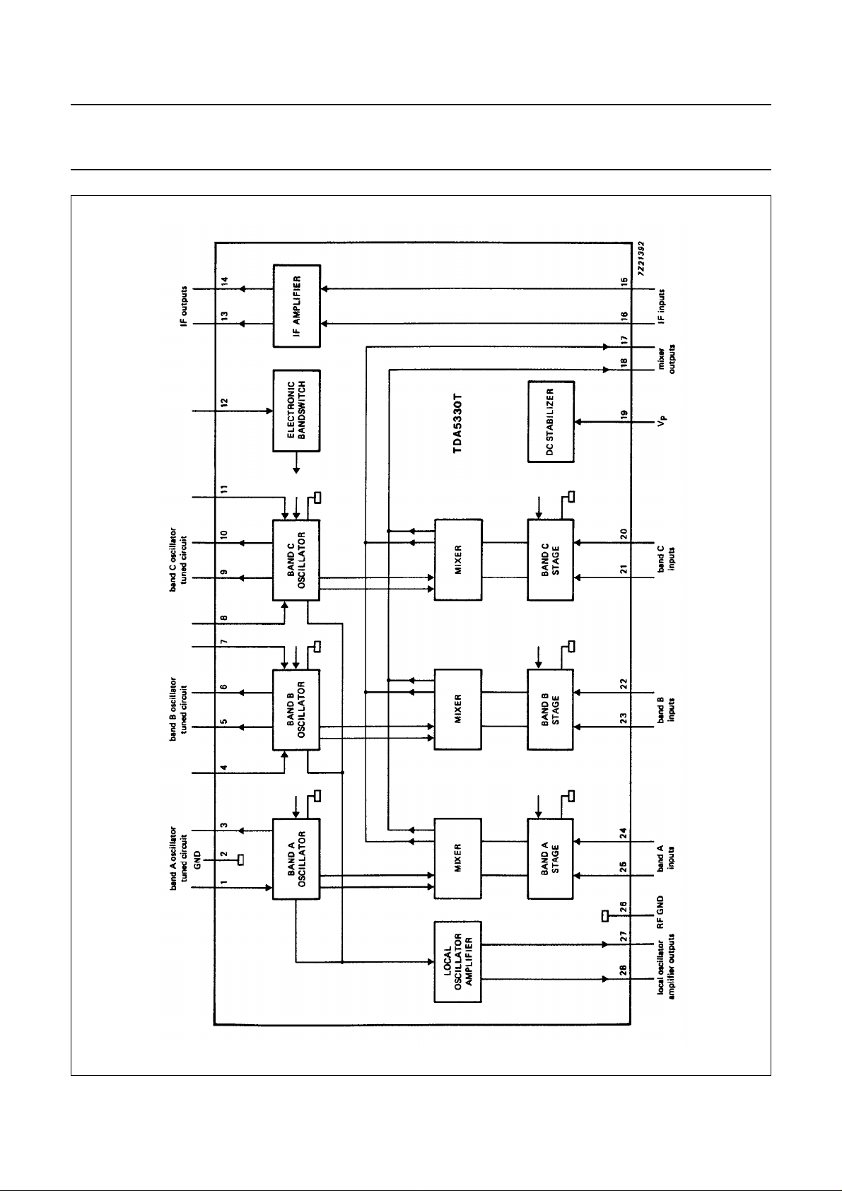
The TDA5330T is a monolithic integrated circuit that performs the band A, band B and band C mixer/oscillator functions
in TV and VCR tuners. This device gives the designer the capability to design an economical and physically small 3-band
tuner which will be capable of meeting the most stringent requirements e.g. FTZ or FCC. The tuner development time
can be drastically reduced by using this device.
Features
• Balanced mixer with a common emitter input for band A
• Amplitude-controlled oscillator for band A
• Balanced mixer with common base input for band B and C
• Balanced oscillator for band B and C
• Local oscillator buffer output for external prescaler
• SAW filter preamplifier with an output impedance of 100 Ω
• Bandgap voltage stabilizer for oscillator stability
• Electronic bandswitch
QUICK REFERENCE DATA
PARAMETER CONDITIONS SYMBOL MIN. TYP. MAX. UNIT
Supply voltage V
Band A frequency range f
Band B frequency range f
Band C frequency range f
19−2, 26
A
B
C
− 12 − V
48 − 180 MHz
160 − 470 MHz
430 − 860 MHz
Conversion noise F 7 − 11 dB
Band A input voltage 1% cross-modulation V
Band B and C input power 1% cross-modulation P
Band A voltage gain G
Band B voltage gain G
Band C voltage gain G
24−26
I
v
v
v
− 100 − dBµV
−−21 − dBm
− 24 − dB
− 37 − dB
− 36 − dB
PACKAGE OUTLINE
28-lead mini-pack , plastic (SO20; SOT163A); SOT 163-1; 1996 November 28.
January 1988 2
Page 3
Philips Semiconductors Product specification
VHF, UHF and Hyperband mixer/oscillator
for TV and VCR 3-band tuners
TDA5330T
January 1988 3
Fig.1 Block diagram.
Page 4
Philips Semiconductors Product specification
VHF, UHF and Hyperband mixer/oscillator
for TV and VCR 3-band tuners
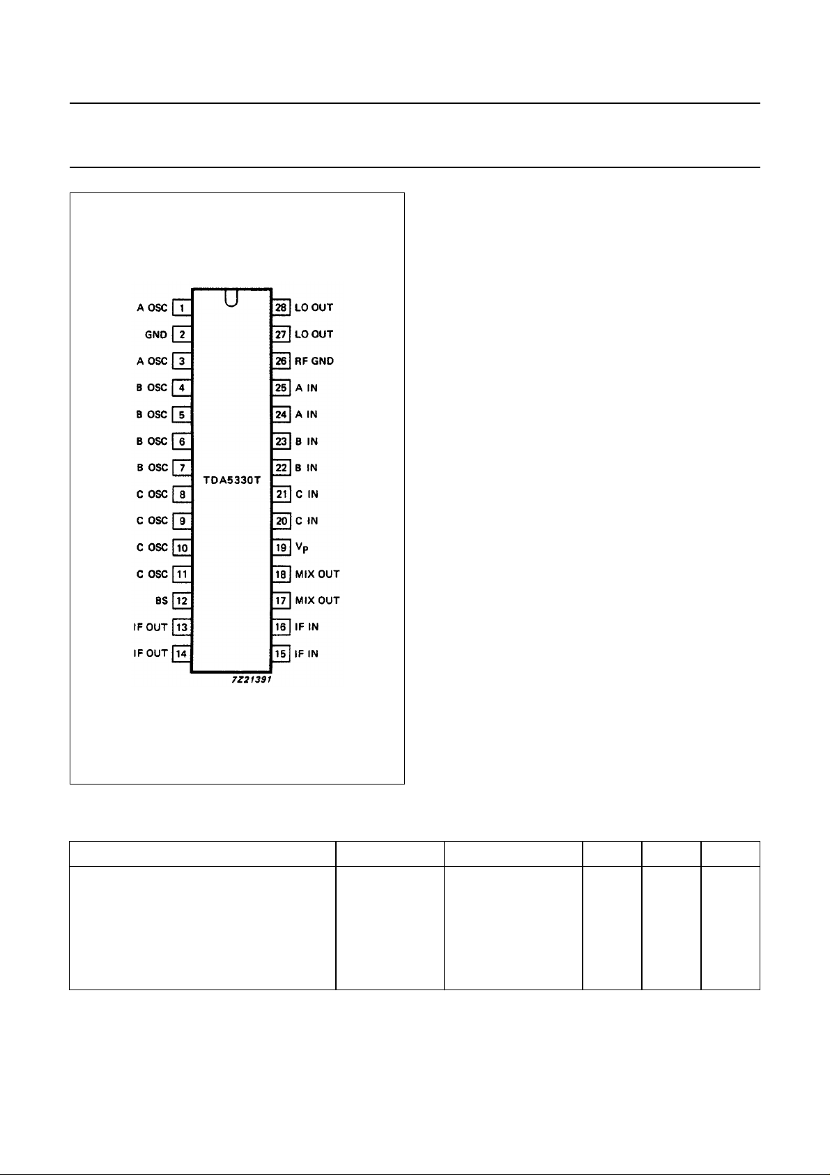
PINNING
1 A OSC band A oscillator input
2 GND ground (0 V)
3 A OSC band A oscillator output
4 B OSC band B oscillator input
5 B OSC band B oscillator output
6 B OSC band B oscillator output
7 B OSC band B oscillator input
8 C OSC band C oscillator input
9 C OSC band C oscillator output
10 C OSC band C oscillator output
11 C OSC band C oscillator input
12 BS electronic bandswitch
13 IF OUT IF amplifier output
14 IF OUT IF amplifier output
15 IF IN IF amplifier input
16 IF IN IF amplifier input
17 MIX OUT mixer output
18 MIX OUT mixer output
19 V
20 C IN band C input
21 C IN band C input
22 B IN band B input
23 B IN band B input
24 A IN band A input
25 A IN band A input
Fig.2 Pinning diagram.
26 RF GND ground for RF inputs
27 LO OUT local oscillator amplifier output
28 LO OUT local oscillator amplifier output
TDA5330T
P
positive supply voltage
RATINGS
Limiting values in accordance with the Absolute Maximum System (IEC 134)
PARAMETER CONDITIONS SYMBOL MIN. MAX. UNIT
Supply voltage V
Switching voltage V
Output current of each pin to ground I
Maximum short-circuit time (all pins) t
Storage temperature range T
Operating ambient temperature range T
P=V19−2, 26
12
O
SC
stg
amb
THERMAL RESISTANCE
From junction to ambient in free air R
th j-a
January 1988 4
−0.3 14 V
014V
−−10 mA
− 10 s
−55 +150 °C
−25 +80 °C
typ. 75 K/W
Page 5

Philips Semiconductors Product specification
VHF, UHF and Hyperband mixer/oscillator
TDA5330T
for TV and VCR 3-band tuners
CHARACTERISTICS
= 12 V; T
V
P
PARAMETER CONDITIONS SYMBOL MIN. TYP. MAX. UNIT
Supply voltage V
Supply current I
Switching voltage;
band A V
band B V
band C V
Switching current;
band C I
Band A Mixer
(including IF amplifier)
Frequency range f
Noise figure note 1;
Optimum source
conductance 50 MHz G
Input admittance see Fig.9
Input capacitance 50 - 180 MHz C
Input voltage 1% cross-modulation;
Input voltage 10 kHz pulling;
Voltage gain 20 log
Band A mixer
Conversion
transadmittance Sc = I
mixer = −I18/V
Mixer output
admittance pins 15 and 16 − 0.1 − mS
Mixer output
capacitance C
=25°C; unless otherwise specified.
amb
measured using
circuit shown in
Fig.9
50 MHz NF − 7.5 9 dB
180 MHz NF − 910dB
180 MHz G
in channel V
in channel V
(V
13−14/V24
)G
17/V24
24
19−2, 26
19
12
12
12
12
A
24−26
24−26
24−26
24−26
24−26
v
Sc
24−17, 18
17−18
10 − 13.2 V
− 42 55 mA
0 − 1.1 V
1.6 − 2.4 V
3.0 − 5.0 V
−−50 µA
48 − 180 MHz
− 0.5 − mS
− 1.1 − mS
− 2 − pF
97 100 − dBµV
100 108 − dBµV
22.5 25.0 27.5 dB
− 3.5 − mS
− 2 − pF
January 1988 5
Page 6

Philips Semiconductors Product specification
VHF, UHF and Hyperband mixer/oscillator
TDA5330T
for TV and VCR 3-band tuners
PARAMETER CONDITIONS SYMBOL MIN. TYP. MAX. UNIT
Band A oscillator
Frequency range f
Frequency shift ∆V
= 10% ∆f −−200 kHz
P
A
Frequency drift ∆T = 25 °C ∆f −−400 kHz
Frequency drift 5 s to 15 min after
switching on ∆f −
Band B mixer
(including IF)
measured using circuit
shown in
Fig.9
measurements
using hybrid;
note 2
Frequency range f
B
Noise figure pins 22 and 23;
200 MHz NF − 810dB
470 MHz NF − 810dB
Input admittance see Fig.5
Available input power 1% cross-modulation;
in channel;
pins 22 and 23;
200 MHz P
470 MHz P
AI
AI
10 kHz pulling pins 22 and 23;
in channel;
470 MHz −−11 − dBm
N+5 − 1 MHz pulling note 3;
430 MHz −−11 − dBm
Voltage gain note 4;
200 MHz G
470 MHz G
v
v
Band B oscillator
Frequency range f
Frequency shift ∆V
= 10% ∆f −−400 kHz
P
B
Frequency drift ∆T=25°C ∆f −−500 kHz
Frequency drift 5 s to 15 min after
switching on ∆f −−200 kHz
80 − 216 MHz
−
200 kHz
160 − 470 MHz
−24 −21 − dBm
−24 −21 − dBm
33 36 39 dB
33 36 39 dB
200 − 500 MHz
January 1988 6
Page 7

Philips Semiconductors Product specification
VHF, UHF and Hyperband mixer/oscillator
TDA5330T
for TV and VCR 3-band tuners
PARAMETER CONDITIONS SYMBOL MIN. TYP. MAX. UNIT
Band C mixer
(including IF)
Frequency range f
Noise figure pins 20 and 21;
Input admittance see Fig.6
Available input power 1% cross-modulation
10 kHz pulling pins 20 and 21;
N+5 − 1 MHz pulling note 3;
Voltage gain note 4;
Band C oscillator
Frequency range f
Frequency shift ∆V
Frequency drift ∆T=25°C ∆f −−800 kHz
Frequency drift 5 s to 15 min after
IF Amplifier
Input reflection
coefficient S
Reverse transmission
coefficient S
Forward transmission
coefficient S
Output reflection
coefficient see Fig.8 S
measured
using circuit shown in
Fig.9;
measurements
using hybrid;
note 2
C
430 − 860 MHz
430 MHz NF − 911dB
860 MHz NF − 911dB
in channel;
pins 20 and 21;
430 MHz P
860 MHz P
AI
AI
−25 −21 − dBm
−25 −21 − dBm
in channel;
860 MHz −−20 − dBm
820 MHz −42 −35 − dBm
430 MHz G
860 MHz G
= 10% ∆f −−400 kHz
b
v
v
C
33 36 39 dB
33 36 39 dB
470 − 900 MHz
switching on ∆f −−200 kHz
mod. phase
note 5; differentially
measured at 36 MHz;
see Fig.7
11
12
21
22
−−0,5 −2.0 − dB/deg
−−41 −7 − dB/deg
− 12 160 − dB/deg
−−910− dB/deg
January 1988 7
Page 8

Philips Semiconductors Product specification
VHF, UHF and Hyperband mixer/oscillator
TDA5330T
for TV and VCR 3-band tuners
PARAMETER CONDITIONS SYMBOL MIN. TYP. MAX. UNIT
LO output
Output voltage into
50 Ω resistor V
Spurious signal on
LO output with
respect to LO
output signal note 6 SRF −−−10 dB
LO signal harmonics
with respect to
LO signal measured at 50 Ω SHD −−−10 dB
Notes
1. Measured with an input circuit for optimum noise. (see Fig.3).
2. The values have been corrected for hybrid and cable losses. The symmetrical output impedance of the circuit is
100 Ω.
3. The input level of a N+5 − 1 MHz signal (just visible).
4. The gain is defined as the transducer gain (measured in Fig.9) plus the voltage transformation ratio of L6 to L7
(6:1, 16 dB).
5. All S parameters are referred to a 50 Ω system.
6. Measured with 50 Ω output impedance on pins 26 and 27 and a RF input signal level of:
RF level = 1 V at f < 180 MHz
RF power = 0.5 dBm at 100 MHz < f < 225 MHz
RF power = −10 dBm at 225 MHz < f < 860 MHz
27−28
14 35 100 mV
Fig.3 Input circuit for optimum noise.
Table 1 Component values
COMPONENT F = 50 MHz F = 180 MHz
L 13 t, ∅ 5.5 mm, wire 0.7 mm (note 1)
L2 rigid cable, 2.9 cm (note 1)
L3 rigid cable, 4 cm (note 1)
C 9.6 pF (note 1)
Note
1. Value to be fixed.
January 1988 8
Page 9

Philips Semiconductors Product specification
VHF, UHF and Hyperband mixer/oscillator
TDA5330T
for TV and VCR 3-band tuners
Table 2 Electrical parameters of the circuit (for appropriate impedance and selectivity)
PARAMETER F = 50 MHz F = 180 MHz UNIT
Insertion loss 0.3 (note 1) dB
Bandwidth 8 (note 1) MHz
Image suppression 15 (note 1) dB
Output impedance (source for IC) 2 (note 1) kΩ
Note
1. Value to be fixed.
Fig.4 S11 of the band A mixer input (40 to 220 MHz).
January 1988 9
Page 10

Philips Semiconductors Product specification
VHF, UHF and Hyperband mixer/oscillator
for TV and VCR 3-band tuners
TDA5330T
Fig.5 S11 of the band B mixer input (150 to 500 MHz).
Fig.6 S11 of the band C mixer input (450 to 900 MHz).
January 1988 10
Page 11

Philips Semiconductors Product specification
VHF, UHF and Hyperband mixer/oscillator
for TV and VCR 3-band tuners
TDA5330T
Fig.7 S11 of the LO output (50 to 900 MHz).
Fig.8 S11, S12 and S22 of the IF amplifier (30 to 60 MHz).
January 1988 11
Page 12

Philips Semiconductors Product specification
VHF, UHF and Hyperband mixer/oscillator
for TV and VCR 3-band tuners
TDA5330T
January 1988 12
Fig.9 Test circuit diagram.
Page 13

Philips Semiconductors Product specification
VHF, UHF and Hyperband mixer/oscillator
TDA5330T
for TV and VCR 3-band tuners
Component values of the test circuit
resistors
R1 = 47 kΩ R2 = 18 Ω R3 = 22 kΩ R4 = 22 kΩ
R5 = 22 Ω (SMD) R6 = 22 kΩ R7 = 1 kΩ R8 = 2.2 kΩ
R9 = 22 kΩ R10 = 15 kΩ R11 = 22 kΩ
capacitors
C1 = 1 nF C2 = 1 nF C3 = 1 nF C4 = 1 nF
C5 = 1 nF C6 = 1 nF C7 = 1 nF C8 = 1 nF
C9 = 1 nF C10 = 1 nF C11 = 1 nF C12 = 15 pF (N750)
C13 = 15 pF (N750) C14 = 1 nF C15 = 1 nF C16 = 1 nF
C17 = 0.68 pF (SMD) C18 = 1 pF (SMD) C19 = 100 pF (SMD) C20 = 5.6 pF (SMD)
C21 = 1 pF C22 = 0.68 pF (SMD) C23 = 150 pF (N750) C24 = 1.8 pF (N750)
C25 = 3.3 pF (SMD) C26 = 3.3 pF (SMD) C27 = 1.8 pF (SMD) C28 = 1 nF
C29 = 1 pF (NPO) C30 = 1 pF (NPO) C31 = 82 pF (N750) C32 = 1 nF
C33 = 1 µF (40 V) Cm = 18 pF (N750)
diodes and IC
D1 = BB911 D2 = BB909B D3 = BB405B
IC = TDA5330T
coils
L1 = 6.5 t (φ3) L2 = 1.5 t (φ3) L3 = 1.5 t (φ3) L4 = 1.5 t (φ3)
L5 = 2 × 6 t (note 1) L6 = 12 t (note 1) L7 = 2 t (mounted on L6) L8 = 5 µH (choke coil)
wire size for L1 to L4 = 0.4 and for L5 to L7 = 0.1 mm.
Note
1. Coil type: TOKO 7 kN; material: 113 kN, screw core (03-0093), pot core (04-0026).
January 1988 13
Page 14

Philips Semiconductors Product specification
VHF, UHF and Hyperband mixer/oscillator
for TV and VCR 3-band tuners
PACKAGE OUTLINE
SO20: plastic small outline package; 20 leads; body width 7.5 mm
D
c
y
Z
20
11
TDA5330T
SOT163-1
E
H
E
A
X
v M
A
pin 1 index
1
e
0 5 10 mm
DIMENSIONS (inch dimensions are derived from the original mm dimensions)
mm
A
max.
2.65
0.10
A
0.30
0.10
0.012
0.004
1
A2A
2.45
2.25
0.096
0.089
0.25
0.01
b
0.49
0.36
p
cD
0.32
0.23
0.013
0.009
3
0.019
0.014
UNIT
inches
Note
1. Plastic or metal protrusions of 0.15 mm maximum per side are not included.
10
w M
b
p
scale
(1)E(1) (1)
13.0
12.6
0.51
0.49
eHELLpQ
7.6
1.27
7.4
0.30
0.050
0.29
10.65
10.00
0.419
0.394
Q
A
2
A
1
1.4
0.055
1.1
0.4
0.043
0.016
detail X
1.1
1.0
0.043
0.039
(A )
L
p
L
0.25
0.01
A
3
θ
0.25 0.1
0.01
ywv θ
Z
0.9
0.4
8
0.004
0.035
0.016
0
o
o
OUTLINE
VERSION
SOT163-1
IEC JEDEC EIAJ
075E04 MS-013AC
REFERENCES
January 1988 14
EUROPEAN
PROJECTION
ISSUE DATE
95-01-24
97-05-22
Page 15

Philips Semiconductors Product specification
VHF, UHF and Hyperband mixer/oscillator
TDA5330T
for TV and VCR 3-band tuners
SOLDERING
Introduction
There is no soldering method that is ideal for all IC packages. Wave soldering is often preferred when through-hole and
surface mounted components are mixed on one printed-circuit board. However, wave soldering is not always suitable for
surface mounted ICs, or for printed-circuits with high population densities. In these situations reflow soldering is often
used.
This text gives a very brief insight to a complex technology. A more in-depth account of soldering ICs can be found in our
“IC Package Databook”
Reflow soldering
Reflow soldering techniques are suitable for all SO packages.
Reflow soldering requires solder paste (a suspension of fine solder particles, flux and binding agent) to be applied to the
printed-circuit board by screen printing, stencilling or pressure-syringe dispensing before package placement.
Several techniques exist for reflowing; for example, thermal conduction by heated belt. Dwell times vary between
50 and 300 seconds depending on heating method. Typical reflow temperatures range from 215 to 250 °C.
Preheating is necessary to dry the paste and evaporate the binding agent. Preheating duration: 45 minutes at 45 °C.
(order code 9398 652 90011).
Wave soldering
Wave soldering techniques can be used for all SO packages if the following conditions are observed:
• A double-wave (a turbulent wave with high upward pressure followed by a smooth laminar wave) soldering technique
should be used.
• The longitudinal axis of the package footprint must be parallel to the solder flow.
• The package footprint must incorporate solder thieves at the downstream end.
During placement and before soldering, the package must be fixed with a droplet of adhesive. The adhesive can be
applied by screen printing, pin transfer or syringe dispensing. The package can be soldered after the adhesive is cured.
Maximum permissible solder temperature is 260 °C, and maximum duration of package immersion in solder is
10 seconds, if cooled to less than 150 °C within 6 seconds. Typical dwell time is 4 seconds at 250 °C.
A mildly-activated flux will eliminate the need for removal of corrosive residues in most applications.
Repairing soldered joints
Fix the component by first soldering two diagonally- opposite end leads. Use only a low voltage soldering iron (less
than 24 V) applied to the flat part of the lead. Contact time must be limited to 10 seconds at up to 300 °C. When using a
dedicated tool, all other leads can be soldered in one operation within 2 to 5 seconds between 270 and 320 °C.
January 1988 15
Page 16

Philips Semiconductors Product specification
VHF, UHF and Hyperband mixer/oscillator
TDA5330T
for TV and VCR 3-band tuners
DEFINITIONS
Data sheet status
Objective specification This data sheet contains target or goal specifications for product development.
Preliminary specification This data sheet contains preliminary data; supplementary data may be published later.
Product specification This data sheet contains final product specifications.
Limiting values
Limiting values given are in accordance with the Absolute Maximum Rating System (IEC 134). Stress above one or
more of the limiting values may cause permanent damage to the device. These are stress ratings only and operation
of the device at these or at any other conditions above those given in the Characteristics sections of the specification
is not implied. Exposure to limiting values for extended periods may affect device reliability.
Application information
Where application information is given, it is advisory and does not form part of the specification.
LIFE SUPPORT APPLICATIONS
These products are not designed for use in life support appliances, devices, or systems where malfunction of these
products can reasonably be expected to result in personal injury. Philips customers using or selling these products for
use in such applications do so at their own risk and agree to fully indemnify Philips for any damages resulting from such
improper use or sale.
January 1988 16
 Loading...