

Page 1
[Q)~u~
~[}{]~~¥
.
Product specification
File under Integrated Circuits, ICO1
Philips
Semiconductors
November 96
re
Page 2
Philips Semiconductors
Product specification
Brushless DC motor drive circuit
FEATURES
.Full-wave commutation (using push/pull drivers at the output stages) without position sensors
.Built-in start-up circuit
.Optimum commutation independent on motor type or motor loading
.Built-in flyback diodes
.Three push-pull outputs:
-0.85 A output current
-built-in current limiter
.Thermal protection
.Low current consumption by adaptative base-drive
.Tacho output without extra sensor.
..Comparator for external position generator (PG) signal
.Built-in multiplexer combining internal FG and external PG signal on one pin for easy use with a controlling
microprocessor
.Linear control of the output stages
.PG signal output.
TDA5241
APPLICATIONS
.General purpose spindle driver ( e.g. VCR scanner motor).
GENERAL DESCRIPTION
The TDA5241 is a bipolar integrated circuit used to drive brush less DC motors in full-wave mode. The device senses the
rotor position using an EMF-sensing technique and is ideally suited as a drive circuit for VCR scanner motors.
QUICK REFERENCE DATA
~ Measured over full voltage and temperature ranges
SYMBOL
Yp
IUM
Yo
Note
1. An unstabilized supply can be used; Transients of 2 V allowed with max slope 0.1 V/J.ls.
supply voltage range (note 1 } 4
I cu!rent limiting
I oU~Ut voltage at 10 = 100 mA(Upper+Lower transistor)
PARAMETER MIN. TYP.
0.6
0.85
0.93
MAX.
~
~
UNIT
v
A
V
2/19
Page 3
Philips Semiconductors
Product specification
Brushless DC motor drive circuit
ORDERING INFORMATION
.
TDA5241
.
March 1997
Fig.1 Power derating curve .
3/19
Page 4
Philips Semiconductors
8
Brushless DC motor drive circuit
BLOCK DIAGRAM
Product specification
TDA5241
March 1997
4/19
Page 5
Philips Semiconductors
Product specification
Brushless DC motor drive circuit
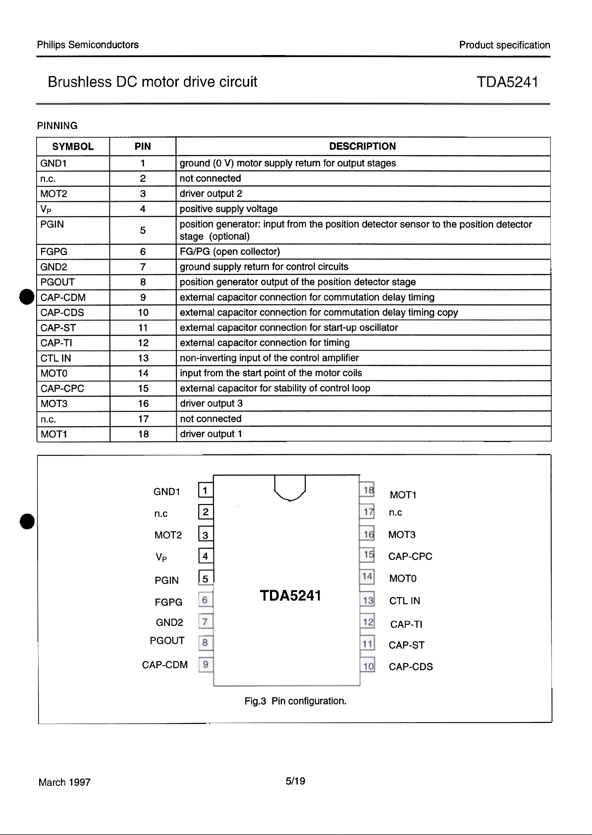
PINNING
SYMBOL PIN
8
GND1
n.c.
MOT2
Vp
PGIN
FGPG
GND2
PGOUT
CAP-CDM
CAP-CDS
CAP-ST
CAP- TI
CTLIN
MOTO
CAP-CPC
MOT3
n.c.
MOT1
1
2
3
4
5
6
7
8
9
10
11
12
13
14
15
16
17
18
ground (0 V) motor supply return for output stages
not connected
driver output 2
Dositive suDDlv voltage
position generator: input from the position detector sensor to the position detector
stage (optional)
FG/PG (open collector)
ground supply return for control circuits
position generator output of the position detector stage
external capacitor connection for commutation delay timing
external capacitor connection for commutation delay timing copy
external capacitor connection for start-up oscillator
external capacitor connection for timing
non-inverting input of the control amplifier
input from the start point of the motor coils
external capacitor for stability of control loop
driver output 3
I not connected
I driver output 1
TDA5241
DESCRIPTION
GND1
n.c
.
u
MOT2
Vp
PGIN
FGPG
GND2
PGOUT
CAP-CDM
10 I
6
7
18
19
TDA5241
18
MOT1
17 n.c
16 MOT3
15
CAP-CPC
14
MOTO
CTLIN
13
12
CAP- TI
CAP-ST
111
CAP-CDS
110
Fig.3 Pin configuration.
March 1997
5/19
Page 6
Philips Semiconductors
Product specification
Brushless DC motor drive circuit
TDA5241
FUNCTIONAL DESCRIPTION
The TDA5241 offers a sensorless three phase motor drive function. It is unique in its combination of sensorless motor
drive and full-wave drive.
The TDA5241 offers protected outputs capable of handling high currents and can be used with star or delta connected
motors. It can easily be adapted for different motors and applications.
The TDA5241 offers the following features:
.Sensorless commutation by using the motor EMF
.Built-in start-up circuit
.Optimum commutation, independent of motor type or motor loading
.Built-in flyback diodes
.Three phase full-wave drive
..High output current (0.85 A)
.Outputs protected by current limiting and thermal protection of each output transistor
.Low current consumption by adaptive base-drive
.Accurate frequency generator (FG) by using the motor EMF
.Comparator for external position generator (PG) signal
.Built-in multiplexer combining internal FG and external PG signals on one pin for easy use with a controlling
microprocessor
.Linear control of the output stages.
LIMITING VALUES
In accordance with the Absolute Maximum Rating System (IEC 134).
PARAMETER
8
SYMBOL
Vp
VI
1 0
Vo
VI
Ptot
~
Tamb
supply voltage
input voltage; all pins except Vp (VI < 8 V)
output voltage; PGOUT and PG/FG
output voltage; MOTO, MOT1, MOT2 and MOT3
input voltage; CAP-ST, CAP- TI, CAP-CD and CAP-DC
total power dissipation
storage temperature range
I operating ambient temperature range
-0.3
GND
-1
~
1-10
MIN.
MAX.
18
I
V p + 0.5
Vp
Vp + Vo
2.5
see power
derating
curve
+150
+70
.5
UNIT
v
v
v
v
v
loc
~
March 1997
6/19
Page 7

Philips Semiconductors Product specification
TDA5241Brushless DC motor drive circuit
CHARACTERISTICS
VP = 14.5 V "10%; T
Symbol
Supply
V
P
I
P
Thermal protection
T
SD
DT
MOT0 – CENTER TAP
V
I
I
I
V
CSW
DV
CS
V
H
MOT1, MOT2 AND MOT3
V
DO
DV
OL
DV
OH
I
LIM
V
DHF
V
DLF
I
DM
CTL IN
V
CTLIN
V
CTLIN0
G
TRAN
PG IN
V
I
I
B
R
I
V
CSW
+/–V
IAMP
= –10 °C to 70°C, unless otherwise specified
amb
Parameter Conditions Min Typ Max Unit
Supply voltage range note 1 4 – 18 V
Input current range note 2 – 5.3 7 mA
Local temperature at temperature
130 140 150 °C
sensor causing shut–down
Reduction in temperature
after shut–down – TSD–30 – °C
before switch–on
Input voltage range –0.5 – V
Input bias current 0.5 V<VI <VP–1.5 V –10 – –
P
V
mA
Comparator Switching Level note 3 20 30 40 mV
Variations in comparator switching
–3 0 +3 mV
levels
Comparator input hysteresis – 75 –
mV
Voltage drop at 25 °C IO = 100 mA – 0.93 1.05 V
(V
upper stage + V
out
Variation in voltage between lower
transistors
Variation in voltage between upper
transistors
Current limiting
Diode forward voltage (DH) notes 4 and 5; see Fig. 2;
Diode forward voltage (DL) notes 4 and 5; see Fig. 2;
lower stage) IO = 500 mA – 1.65 1.9
out
in control mode;
= 100 mA
I
O
in control mode;
I
= –100 mA
O
12 V/6.8W
– – 150 mV
– – 150 mV
0.6 0.85 1 A
– – 1.5 V
I
= –500 mA
O
–1.5 – – V
I
= 500 mA
O
Peak diode current note 5 – – 1 A
Input voltage range 0 – V
Offset voltage See Fig. 6
V
CAPCPC
v 1.1 V
Transfer gain CAP–CPC = 100 nF
V
= 1.5V and
CTLIN
V
= 3 V
CTLIN
0.7 – – V
4.5 5 5.5 V/V
P
V
Input voltage range –0.3 – +5 V
Input bias current – – 650 nA
Input resistance 5 – 30
kW
Comparator switching level 86 93 107 mV
Comparator input hysteresis – 8 – mV
March 1997
7/19
Page 8

Philips Semiconductors Product specification
TDA5241Brushless DC motor drive circuit
Symbol UnitMaxTypMinConditionsParameter
PG OUT (open collector)
V
OL
V
OHmax
t
THL
t
PL
FG/PG (open collector)
V
OL
V
OHmax
t
THL
d
t
PL
CAP–ST
I
I
I
O
V
SWL
V
SWM
V
SWH
CAP–TI
I
I
I
OH
I
OL
V
SWL
V
SWM
V
SWH
CAP–CDM
I
I
I
O
II/I
O
V
IL
V
IH
Output voltage LOW IO = 1.6 mA – – 0.4 V
Output voltage HIGH – – V
Transition time HIGH-to-LOW;
– 0.5 –
P
V
ms
CL = 50 pF;
RL = 10 kW
Pulse width LOW 4 – 10
ms
Output voltage LOW IO =1.6 mA – – 0.4 V
Maximum output voltage HIGH – – V
Transition time HIGH–to–LOW
– 0.5 –
P
V
ms
CL = 50 pF
RL = 10 kW
Ratio of FG frequency and
– 1:2 – –
commutation frequency
Duty factor – 50 – %
Pulse width LOW after a PG IN pulse 5 7 15
Output sink current 1.5 2.0 2.5
Output source current –2.5 –2.0 –1.5
ms
mA
mA
Lower switching level – 0.20 – V
Middle switching level – 0.30 – V
Upper switching level – 2.20 – V
Output sink current 22 30 38
Output source current HIGH –70 –63 –56
Lower source current LOW –6.0 –5.3 –4.6
mA
mA
mA
Lower switching level – 50 – mV
Middle switching level – 0.30 – V
Upper switching level – 2.20 – V
Output sink current 10.6 16.2 22
Output source current –5.3 –8.1 –11
mA
mA
Ratio of sink to source current 1.85 2.05 2.25
Input voltage level LOW 780 860 940 mV
Input voltage level HIGH 2.3 2.4 2.55 V
March 1997
8/19
Page 9

Philips Semiconductors Product specification
TDA5241Brushless DC motor drive circuit
Symbol UnitMaxTypMinConditionsParameter
CAP–CDS
I
I
I
O
II/I
O
V
IL
V
IH
CAP–CPC
I
I
I
O
NOTES:
1. An unstabilized supply can be used; transients of 2 V allowed with max slope 0.1 V/µs.
2. All other inputs at 0V; all outputs at V
3. Switching levels with respect to MOT1, MOT2 and MOT3.
4. Drivers are in high impedance OFF–state.
5. The outputs are short–circuit protected by limiting the current and the IC temperature.
Output sink current 10.1 15.5 20.9
Output source current –20.9 –15.5 –10.1
A
A
Ratio of sink to source current 0.9 1.025 1.15
Input voltage level LOW 780 860 940 mV
Input voltage level HIGH 2.3 2.4 2.55 V
Output sink current 1 – 3 mA
Output source current –100 – –30
and IO = 0 µA.
P
A
March 1997
Fig. 4 Switching levels
9/19
Page 10

Product specificationPhilips Semiconductors
8
Brushless DC motor drive circuit
TDA5241
APPLICATION INFORMATION
Introduction
Figure 5 shows full-wave driving of a three phase motor requires three push-pull output stages. In each of the six possible
states two outputs are active, one sourcing and one sinking current. The third output presents a high impedance to the
motor which enables measurement of the motor EMF in the corresponding motor coil by the EMF comparator at each
output. The commutation logic is responsible for control of the output transistors and selection of the correct EMF
comparator.
The zero-crossing in the motor EMF (detected by the comparator selected by the commutation logic) is used to calculate
the correct moment for the next commutation, that is, the change to the next output state. The delay is calculated
(depending on the motor loading) by the adaptive commutation delay block.
Because of high inductive loading the output stages contain flyback diodes. The output stages are also protected by a
current limiting circuit and by thermal protection of the six output transistors.
8 The zero-crossings can be used to provide speed information such as the tacho signal FG. A VCR scanner also requires
a PG phase sensor. This circuit has an interface for a simple pick-up coil. A multiplexer circuit is also provided to combine
the FG and PG signals in time. The TDA 5240 is providing 1 multiplexed FG PG signal: pin7 (8020) FG-PG 3 times the
number of pole pairs. A PG output signal is generated; pulse width is typically 7 ~s.
Table 1
8 In Table1 , the sequence of the six possible states of the outputs has been depicted
OUTPUT STATES
STATE
1
2
3
4
5
6
MOT1
Z
H
H
Z
L
L
MOT2
L
L
Z
H
H
Z
MOT3
H
Z
L
L
Z
-
H
8
March 1997
10/19
Page 11

Philips Semiconductors
Brushless DC motor drive circuit TDA5241
.
Product specification
.
March 1997
Fig.5 Typical application of the TDA5241.
11/19
Page 12

Philips Semiconductors
Product specification
Brushless DC motor drive circuit TDA5241
Analog control of the motor output voltages is achieved by an internal operational amplifier which tranfer gain is internally
fixed. Compensation of the motor pole is done by an external capacitor (CAP CPC).
Both grounds GND1 and GND2 must be connected together.
ADJUSTMENTS
The system has been designed in such a way that the tolerances of the application components are not critical. However ,
the approximate values of the following components must still be determined:
.The start capacitor; this determines the frequency of the start oscillator
.The two capacitors in the adaptive commutation delay circuit. These are important in determining the optimum moment
for commutation, depending on the type and loading of the motor
.The timing capacitor; this provides the system with its timing signals
(This deals with the application note AN94070)
THE START CAPACITORS (CAP-ST)
This capacitor determines the frequency of the start oscillator. It is charged and discharged, with a current of 2 ~A, from
0.05 to 2.2 V and back to 0.05 V. The time taken to complete one cycle is given by:
tstart = (2.15 X C)s (with C in ~F)
The start oscillator is reset by a commutation pulse and so is only active when the system is in the start-up mode. A pulse
from the start oscillator will cause the outputs to change to the next state (torque in the motor) .If the movement of the
motor generates enough EMF the TDA5241 will run the motor. If the amount of EMF generated is insufficient, then the
motor will move one step only and will oscillate in its new position.
The amplitude of the oscillation must decrease sufficiently before the arrival of the next start pulse, to prevent the pulse
arriving during the wrong phase of the oscillation. The oscillation of the motor is given by:
8
March 1997
12/19
Page 13

Philips Semiconductors
Product specification
Brushless DC motor drive circuit
fosc =
where:
Kt = torque constant (N.m/A)
I = current (A)
p = number of magnetic pole-pairs
J = inertia J (kg/m2)
Example: J = 72 x 10-6 kg/m2, K = 25 x 10-3 N.m/A, p = 6 and I = 0.5 A; this gives f osc = 5 Hz. If the damping is high
then a start frequency of 2 Hz can be chosen or t = 500 ms, thus C = 0.5/2 = 0.25 IlF, (choose 220 nF).
TDA5241
THE ADAPTIVE COMMUTATION DELAY (CAP-CDM AND CAP-CDS)
In this circuit capacitor CAP-CDM is charged during one commutation period, with an interruption of the charging current
during the diode pulse. During the next commutation period this capacitor (CAP-CDM) is discharged at twice the charging
current. The charging current is 8.1 IlA and the discharging current 16.2 IlA ; the voltage range is from 0.9 to 2.2 V. The
voltage must stay within this range at the lowest commutation frequency of interest, fc1:
c = 8.1 -5
:rx1:3
If the frequency is lower, then a constant commutation delay after the zero-crossing is generated by the discharge from
2.2 to 0.9 Vat 16.2 J.lA.
-~ (C in nF)
-fC1
maximum delay = (0.076 x C) ms (witch C in nF)
Example: nominal commutation frequency = 900 Hz and the lowest usable frequency = 400 Hz, so:
CAP-CDM = 400= 15.6 (choose 18 nF)
6231
The other capacitor, CAP-CDS, is used to repeat the same delay by charging and discharging with 20 ~A.
The same value can be chosen as for CAP-CDM. Figure 7 illustrates typical voltage waveforms
-Vmax=Vih
voltage
on CAP-CD
-Vil
8
March 1997
Fig.7 CAP-CD and CAP-DC typical voltage waveforms in normal running mode.
(ZCR = Zero-crossing ; COM = COMMUTATION)
13/19
Page 14

Philips Semiconductors
Product specification
Brushless DC motor drive circuit TDA5241
THE TIMING CAPACITOR (CAP- TI)
Capacitor CAP- TI is used for timing the successive steps within one commutation period; these steps include some
internal delays.
The most important function is the watchdog time in which the motor EMF has to recover from a negative diode-pulse
back to a positive EMF voltage (or vice versa). A watchdog timer is a guarding function that only becomes active when
the expected event does not occur within a predetermined time.
The EMF usually recovers within a short time if the motor is running normally ( « ms ). However, if the motor is
motionless or rotating in the reverse direction, then the time can be longer ( » ms ).
A watchdog time must be chosen so that it is long enough for a motor without EMF (still) and eddy currents that may
stretch the voltage in a motor winding; however, it must be short enough to detect reverse rotation. If the watchdog time
is made too long, then the motor may run in the wrong direction (with little torque).
The capacitor is charged, with a current of 5711A, from 0.2 to 0.3 V. Above this level it is charged, with a current of 5 I1A,
up to 2.2 V only if the selected motor EMF remains in the wrong polarity (watchdog function). At the end, or, if the motor
voltage becomes positive, the capacitor is discharged with a current of 28 11 A. The watchdog time is the time taken to
charge the capacitor, with a current of 5 I1A, from 0.3 to 2.2 V. The value of CAP- TI is given by:
= 2.63 tm (C in nF ; t in ms)
Example: If after switching off, the voltage from a motor winding is reduced, in 3.5 ms, to within 20 mV (the offset of the
EMF comparator), then the value of the required timing capacitor is given by:
C = 2.63 x 3.5 = 9.2 (choose 10 nF)
Typical voltage waveforms are illustrated by Fig. 8.
voltage
on CAP- TI
8
March 1997
If the chosen value of CAP- TI is too small, then oscillations can occur in certain positions of a blocked rotor. If the chosen value is too large, then it is
possible that the motor may run in the reverse direction (synchronously with little torque).
Fig.8 Typical CAP- TI and VMOT1 voltage waveforms in normal running mode.
14/19
Page 15

Product specificationPhilips Semiconductors
Brushless DC motor drive circuit
OTHER DESIGN ASPECTS
There are other design aspects concerning the application of the TDA5241 besides the commutation function. They are:
.Generation of the tacho signal FG
.Built-in interface for a PG sensor
.Reliability.
TDA5241
FG SIGNAL
The FG signal is generated in the TDA5241 by using the zero-crossing of the motor EMF from the three motor windings.
Every zero-crossing in a (star connected) motor winding is used to toggle the FG output signal. The FG frequency is
therefore half the commutation frequency. All transitions indicate the detection of a zero-crossing (except for PG). The
negative-going edges are called FG pulses because they generate an interrupt in a controlling microprocessor.
8 The accuracy of the FG output signal Uitter) is very good. This accuracy depends on the symmetry of the motor's
electromagnetic construction, which also effects the satisfactory functioning of the motor itself.
Two FG frequencies are given out: 6 times the number of poles pairs or 3 times the number of poles pairs. A pull-up
resistor must be connected to PGFG outputs
Example: A three phase motor with 6 magnetic pole-pairs at 1500 rpm and with a full-wave drive has a commutation
frequency of 25 x 6 x 6 = 900 Hz, and generates a tacho signal of 450 Hz.
PG SIGNAL
The accuracy of the PG signal in applications such as VCR must be high (phase information. This accuracy is obtained
by combining the accurate FG signal with the PG signal by using a wide tolerance external PG sensor. The external PG
signal (PGIN) is only used as an indicator to select a particular FG pulse. This pulse differs from the other FG pulses in
that a ahort LOW-time of 15 /.ls after a HIGH to LOW transition. All other FG pulses have a 50% duty factor (see Fig. 9),
tolerance on PC IN
PG IN
MOT3
PG / F G.S'-J~s-LJ~
v!\v v!\v
March 1997
Fig.9 Timing and the FG and PG IN signals.
15/19
Page 16

Philips Semiconductors
Product specification
Brushless DC motor drive circuit
RELIABILITY
It is necessary to protect high current circuits and the output stages are protected in two ways:
.Current limiting of the 'lower' output transistors. The 'upper' output transistors use the same base current as the
conducting 'lower' transistor (+15%). This means that the current to and from the output stages is limited.
.Thermal protection of the six output transistors is achieved by each transistor having a thermal sensor that is active
when the transistor is switched on. The transistors are switched off when the local temperature becomes too high.
TDA5241
March 1997
16/19
Page 17

Philips Semiconductors
Product specification
Brushless DC motor drive circuit
PACKAGE OUTLINE
8
TDA5241
Dimensions in mm
MSA259
March 1997
Fig.10 PLASTIC DUAL IN-LINE PACKAGE; 18 LEADS; SOT102RG4
17/19
Page 18

Philips Semiconductors
Product specification
Brushless DC motor drive circuit
SOLDERING
Introduction
There is no soldering method that is ideal for aIlIC packages. Wave soldering is often preferred when through-hole and
surface mounted components are mixed on one printed-circuit board. However, wave soldering is not always suitable for
surface mounted ICs, or for printed-circuits with high population densities. In these situations reflow soldering is often
used.
This text gives a very brief insight to a complex technology. A more in-depth account of soldering ICs can be found in our
"IC Package Databook"(order code 939865290011).
Reflow soldering
Reflow soldering techniques are suitable for all SO packages.
Reflow soldering requires solder paste (a suspension of fine solder particles, flux and binding agent) to be applied to the
printed-circuit board by screen printing, stencilling or pressure-syringe dispensing before package placement.
Several techniques exist for reflowing; for example, thermal conduction by heated belt. Dwell times vary between
50 and 300 seconds depending on heating method. Typical reflow temperatures range from 215 to 250 °C.
Preheating is necessary to dry the paste and evaporate the binding agent. Preheating duration: 45 minutes at 45 °C.
TDA5241
Wave soldering
Wave soldering techniques can be used for all SO packages if the following conditions are observed:
.A double-wave (a turbulent wave with high upward pressure followed by a smooth laminar wave) soldering technique
should be used.
.The longitudinal axis of the package footprint must be parallel to the solder flow.
.The package footprint must incorporate solder thieves at the downstream end.
During placement and before soldering, the package must be fixed with a droplet of adhesive. The adhesive can be
applied by screen printing, pin transfer or syringe dispensing. The package can be soldered after the adhesive is cured.
Maximum permissible solder temperature is 260 °C, and maximum duration of package immersion in solder is
10 seconds, if cooled to less than 150 °C within 6 seconds. Typical dwell time is 4 seconds at 250 °C.
A mildly-activated flux will eliminate the need for removal of corrosive residues in most applications.
Repairing soldered joints
Fix the component by first soldering two diagonally- opposite end leads. Use only a low voltage soldering iron (less
than 24 V) applied to the flat part of the lead. Contact time must be limited to' 10 seconds at up to 300 °C. When using a
dedicated tool, all other leads can be soldered in one operation within 2 to 5 seconds between 270 and 320 °C.
March 1997
18/19
Page 19

Philips Semiconductors Product specification
TDA5241Brushless DC motor drive circuit
Data sheet status
Product
Data sheet status
Objective
specification
Preliminary
specification
Product
specification
[1] Please consult the most recently issued data sheet before initiating or completing a design.
[2] The product status of the device(s) described in this data sheet may have changed since this data sheet was published. The latest information is available on the Internet at URL
http://www.semiconductors.philips.com.
[1]
status
Development
Qualification
Production
[2]
Definitions
Short-form specification — The data in a short-form specification is extracted from a full data sheet with the same type number and title. For
detailed information see the relevant data sheet or data handbook.
Limiting values definition — Limiting values given are in accordance with the Absolute Maximum Rating System (IEC 60134). Stress above one
or more of the limiting values may cause permanent damage to the device. These are stress ratings only and operation of the device at these or
at any other conditions above those given in the Characteristics sections of the specification is not implied. Exposure to limiting values for extended
periods may affect device reliability.
Application information — Applications that are described herein for any of these products are for illustrative purposes only. Philips
Semiconductors make no representation or warranty that such applications will be suitable for the specified use without further testing or
modification.
Disclaimers
Life support — These products are not designed for use in life support appliances, devices or systems where malfunction of these products can
reasonably be expected to result in personal injury . Philips Semiconductors customers using or selling these products for use in such applications
do so at their own risk and agree to fully indemnify Philips Semiconductors for any damages resulting from such application.
Right to make changes — Philips Semiconductors reserves the right to make changes, without notice, in the products, including circuits, standard
cells, and/or software, described or contained herein in order to improve design and/or performance. Philips Semiconductors assumes no
responsibility or liability for the use of any of these products, conveys no license or title under any patent, copyright, or mask work right to these
products, and makes no representations or warranties that these products are free from patent, copyright, or mask work right infringement, unless
otherwise specified.
Contact information
For additional information please visit
http://www.semiconductors.philips.com . Fax: +31 40 27 24825
For sales offices addresses send e-mail to:
sales.addresses@www.semiconductors.philips.com.
Definitions
This data sheet contains data from the objective specification for product development.
Philips Semiconductors reserves the right to change the specification in any manner without notice.
This data sheet contains data from the preliminary specification. Supplementary data will be
published at a later date. Philips Semiconductors reserves the right to change the specification
without notice, in order to improve the design and supply the best possible product.
This data sheet contains data from the product specification. Philips Semiconductors reserves the
right to make changes at any time in order to improve the design, manufacturing and supply.
Changes will be communicated according to the Customer Product/Process Change Notification
(CPCN) procedure SNW-SQ-650A.
Koninklijke Philips Electronics N.V. 1996
All rights reserved. Printed in U.S.A.
Date of release: 11-96
Document order number: 9397 750 08755
yyyy mmm dd
1
 Loading...