

Page 1

INTEGRATED CIRCUITS
DATA SH EET
TDA1593
IF amplifier/demodulator for
FM car radio receivers
Product specification
Supersedes data of 1995 May 29
File under Integrated Circuits, IC01
1996 Oct 10
Page 2

Philips Semiconductors Product specification
IF amplifier/demodulator for
TDA1593
FM car radio receivers
FEATURES
• Balanced limiting amplifier
• Balanced coincidence demodulator
• Two open-collector stop pulse outputs for
microcomputer tuning control
• Simulated behaviour of ratio detector (internal field
strength and detuning dependent voltage for dynamic
AF signal muting)
• Mono/stereo blend field strength indication control
voltage
• AFC output
• Internal compensation of AF signal total harmonic
distortion (THD)
• Built-in hum and ripple rejection circuits.
QUICK REFERENCE DATA
SYMBOL PARAMETER MIN. TYP. MAX. UNIT
V
P
I
P
V
iIF
V
oAF
S/N signal-to-noise ratio (f
THD total harmonic distortion (f
T
amb
supply voltage (pin 1) 7.5 8.5 12 V
supply current (l2=0) − 20 26 mA
IF input sensitivity for limiting on pin 20 (RMS value) 14 22 35 µV
AF output signal on pin 4 (RMS value) 180 200 220 mV
= 400 Hz; ∆f=±75 kHz) − 82 − dB
m
= 1 kHz; ∆f=±75 kHz) − 0.2 0.6 %
m
operating ambient temperature −40 − +85 °C
GENERAL DESCRIPTION
The TDA1593 provides IF amplification, symmetrical
quadrature demodulation and level detection for quality
FM car radio receivers and is suitable for mono and stereo
reception. It may also be applied to common front ends,
stereo decoders and AM receivers circuits.
All pin numbers mentioned in this data sheet refer to the
SO-version (TDA1593T) unless otherwise specified.
ORDERING INFORMATION
TYPE
NUMBER
NAME DESCRIPTION VERSION
PACKAGE
TDA1593 DIP18 plastic dual in-line package; 18 leads (300 mil) SOT102-1
TDA1593T SO20 plastic small outline package; 20 leads; body width 7.5 mm SOT163-1
1996 Oct 10 2
Page 3
Philips Semiconductors Product specification
IF amplifier/demodulator for
FM car radio receivers
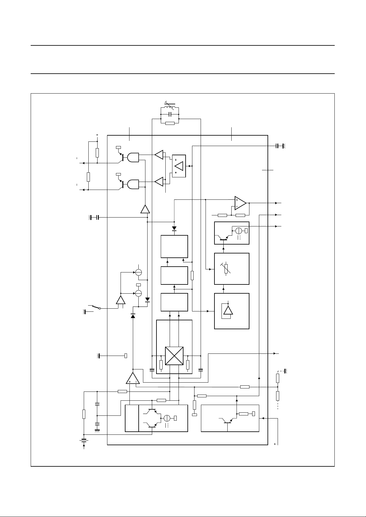
BLOCK DIAGRAM
5 V
25 kΩ
STOP 1
25 kΩ
STOP 0
16 15 14
47 nF
n.c.
12
100
DEMI2
11
pF
TDA1593
DDVWLVLVA ULV V
n.c.
V
ref
oAF
MBE512
100 nF
information
weighted level
MPX signal
=19
3.3
kΩ
DEMI1
10
L
Q
9 n.c.
86754321
TDA1593T
int
V
offset
V
x2
DETUNE
int
V
ref
V
(1)
13
int
V
DETECTOR
HP
FILTER
LP
FILTER
50 kHz
1 MHz
ref
MUTE
25 kΩ
THD
V
ATTENUATOR
COMPENSATION
Fig.1 Block diagram and application circuit.
QUADRATURE
17
9 pF
25 kΩ
18
22 nF
LFB2 LFB1 GND TSW MUTE ST0 ST1
22 nF
19
LEVEL
iIF
20
V
DETECTOR
330 Ω
int
V
25
kΩ
DEMODULATOR
int
V
40 kΩ
LIMITING
AMPLIFIER
9 pF
40
kΩ
VOLTAGE
STABILIZER
information
unweighted level
7.5 kΩ
ref
optional level shift
ref
V
V
SFE
input
FM-IF
1996 Oct 10 3
p ( 8.5 V)
V
(1) Connecting pin 13 to ground is only allowed to measure the current on pin 16; it is not used in application.
Page 4

Philips Semiconductors Product specification
IF amplifier/demodulator for
FM car radio receivers
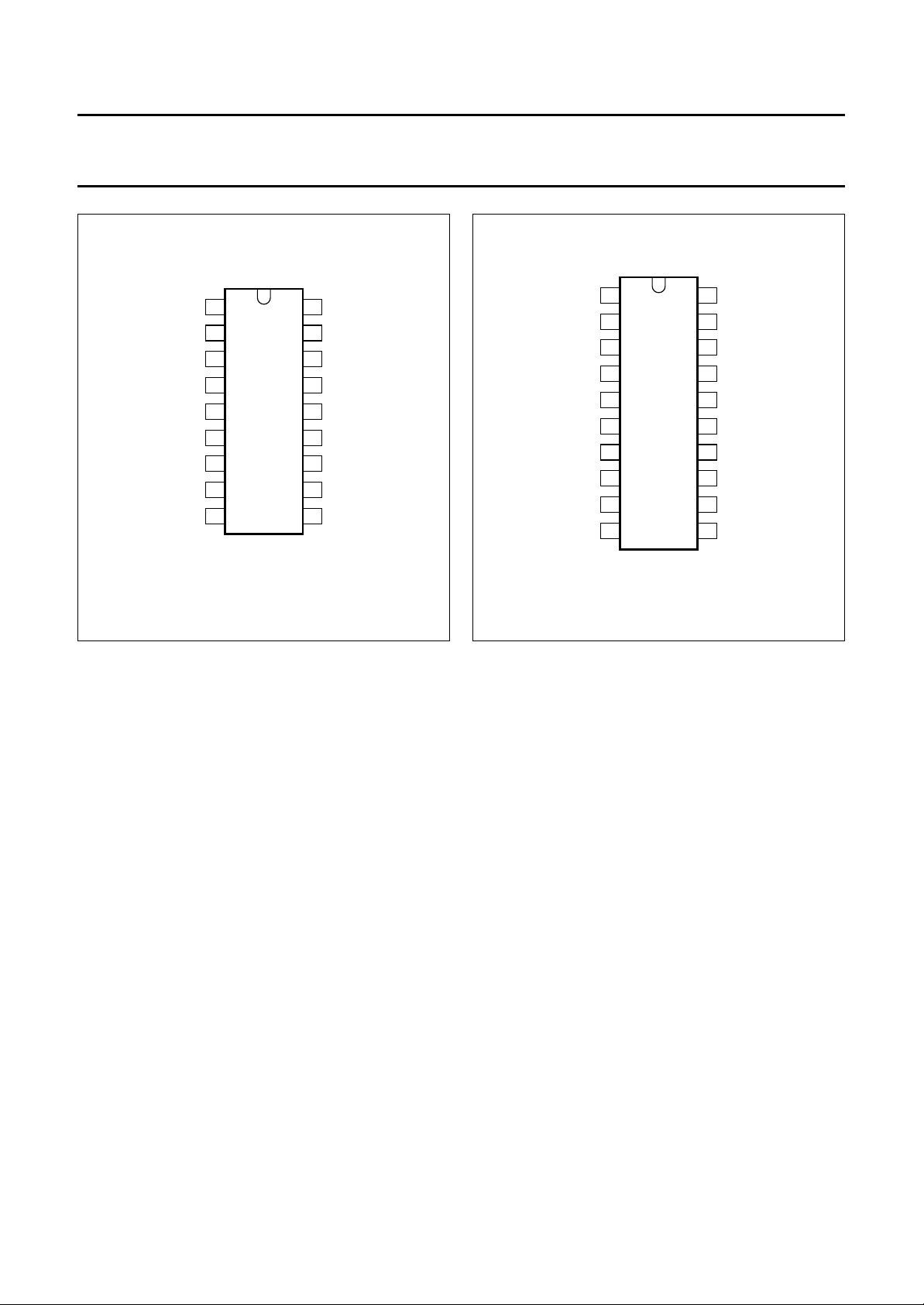
PINNING
PIN
SYMBOL
V
P
LVA 2 2 level adjustment for stop condition
ULV 3 3 unweighted level output
V
oAF
V
ref
WLV 6 6 weighted level output
n.c. 7 7 not connected
DDV 8 8 detune detector voltage
n.c. − 9 not connected
DEMI1 9 10 demodulator input 1
DEMI2 10 11 demodulator input 2
n.c. − 12 not connected
TSW 11 13 tau switch input
ST1 12 14 STOP-1, stop pulse output 1
ST0 13 15 STOP-0, stop pulse output 0
MUTE 14 16 muting voltage
GND 15 17 ground (0 V)
LFB1 16 18 IF limiter feedback 1
LFB2 17 19 IF limiter feedback 2
V
iIF
SOT102-1
DIP18
1 1 supply voltage (+8.5 V)
4 4 audio frequency output (MPX signal)
5 5 reference voltage output
18 20 IF signal input
SOT163-1
SO20
DESCRIPTION
TDA1593
1996 Oct 10 4
Page 5
Philips Semiconductors Product specification
IF amplifier/demodulator for
FM car radio receivers
V
1
P
LVA
2
ULV
3
V
4
oAF
V
5
ref
WLV
n.c.
DDV
DEMI1 DEMI2
TDA1593
6
7
8
9
MBE513
V
18
iIF
17
LFB2
16
LFB1
15
GND
14
MUTE
13
ST0
12
ST1
11
TSW
10
TDA1593
V
1
P
LVA
2
ULV
3
V
4
oAF
V
5
ref
TDA1593T
6
WLV
7
n.c.
8
DDV
n.c. n.c.
9
10
DEMI1 DEMI2
MBE514
V
20
iIF
19
LFB2
18
LFB1
GND
17
16
MUTE
15
ST0
14
ST1
13
TSW
12
11
Fig.2 Pin configuration for DIP-version.
FUNCTIONAL DESCRIPTION
The limiter amplifier has five stages of IF amplification
using balanced differential limiter amplifiers with emitter
follower coupling.
Decoupling of the stages from the supply voltage line and
an internal high-ohmic DC feedback loop give a very stable
IF performance. The amplifier gain is virtually independent
of changes in temperature.
The FM demodulator is fully balanced and compromises
two cross-coupled differential amplifiers.
The quadrature detection of the FM signal is performed by
direct feeding of one differential amplifier from the limiter
amplifier output, and the other via an external 90 degrees
phase shifting network. The demodulator has a good
stability and a small zero-cross-over shift. The bandwidth
of the demodulator output is restricted by an internal
low-pass filter to approximately 1 MHz. Non-linearities,
which are introduced by demodulation, are compensated
by the THD compensation circuit. For this reason, the
demodulator resonance circuit (between pins 10 and 11)
Fig.3 Pin configuration for SO-version.
must have a loaded Q-factor of 19. Consequently, there is
no need for the demodulator tuned circuit to be adjusted
for minimum distortion. Adjustment criterion is a
symmetrical stop pulse. The control voltage for the mute
attenuator (pin 16) is derived from the values of the level
detector and the detuning detector output signals.
The mute attenuator has a fast attack and a slow decay
determined by the capacitor on pin 16. The AF signal is fed
via the mute attenuator to the output (pin 4). A weighted
control voltage (pin 6) is obtained from the mute attenuator
control voltage via a buffer amplifier that introduces an
additional voltage shift and gain.
The level detector generates a voltage output signal
proportional to the amplitude of the input signal.
The unweighted level detector output signal is available.
The open-collector tuning stop output voltages STOP-0
and STOP-1 (pins 15 and 14) are derived from the
detuning and the input signal level. The pins 14 and 15
may be tied together, if only one tuning-stop output is
required.
1996 Oct 10 5
Page 6

Philips Semiconductors Product specification
IF amplifier/demodulator for
TDA1593
FM car radio receivers
LIMITING VALUES
TDA1593T pinning
In accordance with the Absolute Maximum Rating System (IEC 134).
SYMBOL PARAMETER MIN. MAX. UNIT
V
P
V
n
V
13
I
14, 15
P
tot
T
stg
T
amb
V
es
Note
1. Equivalent to discharging a 100 pF capacitor through a 1.5 kΩ series resistor.
supply voltage (pin 1) −0.3 +13 V
voltage at pins 2, 4, 5, 6, 10, 11and 16 −0.3 +10 V
voltage at pins 3, 8, 14, 15, 18, 19 and 20 −0.3 V
P
voltage on pin 13 − 6V
current at pins 14 and 15 − 2mA
total power dissipation − 360 mW
storage temperature −55 +150 °C
operating ambient temperature −40 +85 °C
electrostatic handling; note 1
all pins except pin 5 −2000 +2000 V
pin 5 −2000 +800 V
V
THERMAL CHARACTERISTICS
SYMBOL PARAMETER VALUE UNIT
R
th j-a
thermal resistance from junction to ambient in free air
SOT102-1 80 K/W
SOT163-1 90 K/W
1996 Oct 10 6
Page 7

Philips Semiconductors Product specification
IF amplifier/demodulator for
TDA1593
FM car radio receivers
CHARACTERISTICS
VP= 8.5 V; T
de-emphasis of 50 µs; tuned circuit at pins 10 and 1 1 aligned for symmetrical stop pulses; measurements taken in Fig.4
unless otherwise specified.
SYMBOL PARAMETER CONDITIONS MIN. TYP. MIN. UNIT
V
P
I
P
IF amplifier and demodulator
Z
i
C
i
AF output (pin 4)
R
o
V
4
PSRR power supply ripple rejection
Tuning stop detector
∆f
STOP-0
∆f
STOP-1
V
20
V
14, 15
Reference voltage source (pin 5)
V
ref
R
5
TC temperature coefficient − 3.3 − mV/K
= +25 °C; fIF= 10.7 MHz; deviation ±22.5 kHz with fm= 400 Hz; Vi= 10 mV (RMS) at pin 20;
amb
supply voltage (pin 1) 7.5 8.5 12 V
supply current I2=0 − 20 26 mA
demodulator input impedance
25 40 55 kΩ
between pins 10 and 11
demodulator input capacitance
− 6 − pF
between pins 10 and 11
output resistance − 400 −Ω
DC output level V
(pin 4)
detuning frequency for STOP-0
(pin 15)
detuning frequency for STOP-1
(pin 14)
dependency on input voltage for
STOP-0 and STOP-1
(RMS value)
output voltage I
≤ 5 µV (RMS) on pin 20 2.75 3.1 3.45 V
iIF
f = 1000 Hz;
= 50 mV (RMS)
V
ripple
33 36 − dB
see Fig.9
≥ 3.5 V −−+14.0 kHz
V
15
≤ 0.3 V +22.0 −−kHz
V
15
see Fig.8
≥ 3.5 V −−−14.0 kHz
V
14
≤ 0.3 V −22.0 −−kHz
V
14
see Fig.7
≥ 3.5 V 250 −−µV
V
14, 15
≤ 0.3 V −−50 µV
V
14, 15
=1mA −−0.3 V
14, 15
reference output voltage I5= −1 mA 3.3 3.7 4.1 V
output resistance I5= −1mA − 40 80 Ω
External muting
V
16
S steepness of control voltage
muting voltage at I2=0 V20≤ 5 µV (RMS); see Fig.10 1.45 1.75 2.05 V
= 1 mV (RMS) 3.0 3.45 3.9 V
V
20
slope: 100 µV ≤ V20≤ 100 mV;
20 ∆log V
---------------------
∆ V20log
∆V
20
16
1996 Oct 10 7
− 0.85 − V/dec
=20dB
Page 8

Philips Semiconductors Product specification
IF amplifier/demodulator for
TDA1593
FM car radio receivers
SYMBOL PARAMETER CONDITIONS MIN. TYP. MIN. UNIT
Internal mute α; note 1
α mute voltage V
I
16
current for capacitor (pin 16)
charge current V
discharge current V
charge current V
discharge current V
≥ V
16
ref
= 0.77V
V
16
= 0.55V
V
16
=0V −−8−µA
13
=0V − +120 −µA
13
13=Vref
13=Vref
ref
ref
Level detector
R
6
V
6
output resistance −−500 Ω
output voltage at I2=0 V20≤ 5 µV (RMS); see Fig.11 0.1 − 1.1 V
= 1 mV (RMS) 3.0 − 4.2 V
V
20
±200 kHz detuning 1.2 1.5 1.8 V
∆V
6
output voltage at detuning ±45 kHz detuning −−0.2 V
TC temperature coefficient − 3.3 − mV/K
S steepness of control voltage
slope: 50 µV ≤ V
20 ∆log V
---------------------
∆ V20log
∆V
20
6
20
=20dB
≤ 50 mV;
− 0 − dB
1.5 − 4.5 dB
− 20 − dB
−−100 −µA
− +120 −µA
1.4 1.7 2.0 V/dec
/∆f slope of output voltage at
∆V
6
detuning
S level shift adjustments
range by pin 2 ±∆V
gain −∆V
range by pin 2 ±∆V
gain −∆V
Note
∆V
4FM MUTE– OFF–()
1.
α20
-------------------------------------------------------log=
∆V
4FM MUTE– ON–()
∆f = 125 ±20 kHz − 35 − mV/kHz
6/Vref
/∆V
6
16/Vref
/∆V
16
2
2
0.42 0.5 − V/V
− 1.7 − V/V
0.21 0.25 − V/V
− 0.85 − V/V
1996 Oct 10 8
Page 9

Philips Semiconductors Product specification
IF amplifier/demodulator for
TDA1593
FM car radio receivers
OPERATING CHARACTERISTICS
VP= 7.5 to 12 V; T
de-emphasis of 50 µs; tuned circuit at pins 10 and 1 1 aligned for symmetrical stop pulses; measurements taken in Fig.4
unless otherwise specified.
SYMBOL PARAMETER CONDITIONS MIN. TYP. MIN. UNIT
IF amplifier and demodulator
V
i
S/N signal-to-noise ratio deviation ±75 kHz;
V
o
THD total harmonic distortion deviation ±75 kHz;
α
AM
Tuning stop detector
∆f
STOP-0
∆f
STOP-1
V
20
R
8
V
8
= +25 °C; fIF= 10.7 MHz; deviation ±22.5 kHz with fm= 400 Hz; Vi= 10 mV (RMS) at pin 20;
amb
input signal for start of limiting
V16= 4.5 V 14 22 35 µV
(−3 dB) (RMS value; pin 20)
input signal for signal-to-noise ratio
(RMS value)
f = 250 to 15000 Hz;
= 4.5 V
V
16
S/N=26dB − 15 −µV
S/N=46dB − 60 −µV
− 82 − dB
= 400 Hz
f
m
AF output signal (RMS value; pin 4) 180 200 220 mV
= 1 kHz
f
without de-emphasis − 0.2 0.6 %
m
±25 kHz detuning −−1.0 %
AM suppression on pin 4 m = 30%; on pin 20
= 0.3 to 1000 mV (RMS) 43 55 − dB
V
i
= 1 to 300 mV (RMS) 57 65 − dB
V
i
detuning frequency for STOP-0
(pin 15)
detuning frequency for STOP-1
(pin 14)
dependence on input voltage for
STOP-0 and STOP-1 (RMS value)
internal low-pass resistance of
see Fig.9
≥ 3.5 V −−+14.0 kHz
V
15
≤ 0.3 V +22.0 −−kHz
V
15
see Fig.8
≥ 3.5 V −−−14.0 kHz
V
14
≤ 0.3 V −22.0 −−kHz
V
14
see Fig.7
≥ 3.5 V 250 −−µV
V
14, 15
≤ 0.3 V −−50 µV
V
14, 15
12 25 50 kΩ
detune detector
voltage on capacitor Vi≤ 5 µV (RMS) on
− 2.2 − V
input pin 20
Level detector (I
V
6
=0)
2
output voltage V20≤ 5 µV (RMS) 0.1 − 1.1 V
V
Reference voltage source (pin 5)
V
ref
reference output voltage I5= −1 mA 3.3 3.7 4.1 V
1996 Oct 10 9
= 1 mV (RMS) 3.0 − 4.2 V
20
Page 10

Philips Semiconductors Product specification
IF amplifier/demodulator for
FM car radio receivers
R2
50 Ω
20
12
220 kΩ
22 nF
22 nF
19
S1
S2
IF=10.7 MHz
V
p
(
8.5 V)
R1
150 Ω
10 Ω
100 nF
1817
34
10 kΩ
V
mute STOP 0 STOP 1
47
nF
16
15
5 V
27kΩ27
kΩ
14
TDA1593T
4.7 nF
5
S3
6
3.9 kΩ
7
n.c.
level (weighted)
level (unweighted)
V
oAF
V
ref
V
oAF
89
100
nF
(unweighted)
(3.7 V)
(weighted)
220 nF
n.c.
131211
n.c.
TDA1593
100
3.3
kΩ
10
pF
IF
Q
=19
L
MBE511
Fig.4 Test circuit.
1996 Oct 10 10
Page 11

Philips Semiconductors Product specification
IF amplifier/demodulator for
FM car radio receivers
0
V
4
(dB)
−20
−40
−60
−80
−100
−6
10
(1) Audio signal.
(2) Noise.
(1)
(2)
−5
10
TDA1593
MBE519
−4
10
−3
10
−2
10
−1
10
V
i20 (rms)
(V)
1
Fig.5 Audio signal and noise as functions of the input signal V
de-emphasis 50 µs.
0
V
4
(dB)
−20
−40
−60
−80
−100
−6
10
(1) Audio signal.
(2) Spurious AM signal.
(1)
(2)
−5
10
−4
10
−3
10
(pin 20) with ∆f=±22.5 kHz; fm= 1 kHz;
iIF
−2
10
−1
10
V
i20 (rms)
MBE520
(V)
1
Fig.6 Typical AM suppression as a function of the input signal V
AM with fm= 400 Hz; m = 0.3 and 250 to 15000 Hz bandwidth.
1996 Oct 10 11
(pin 20) with ∆f=±22.5 kHz; fm= 1 kHz;
iIF
Page 12

Philips Semiconductors Product specification
IF amplifier/demodulator for
FM car radio receivers
10
V
14,15
(V)
8
6
4
2
0
−6
10
−5
10
TDA1593
MBE521
−4
10
−3
10
−2
10
−1
10
V
i20 (rms)
(V)
1
Fig.7 STOP-0 and STOP-1 output voltage dependent on input signal V
10
V
14
(V)
8
6
4
2
0
–10
–20 +10
0
MBE522
+20 +30–30
detune (kHz)
10
V
15
(V)
8
6
4
2
0
–10
–20 +10
(pin 20).
iIF
0
MBE523
+20 +30–30
detune (kHz)
Fig.8 STOP-1 output voltage dependent on
V
= 10 mV (RMS) (pin 20).
iIF
1996 Oct 10 12
Fig.9 STOP-0 output voltage dependent on
V
= 10 mV (RMS) (pin 20).
iIF
Page 13

Philips Semiconductors Product specification
IF amplifier/demodulator for
FM car radio receivers
10
V
16
(V)
8
6
4
2
0
10
(1) V2=0V.
(2) I2= 0mA.
(3) V2=V
ref
−6
.
−5
10
TDA1593
MBE515
(1)
(2)
(3)
−4
10
−3
10
−2
10
−1
10
V
i20 (rms)
(V)
1
Fig.10 External mute voltage V16 dependent on input signal V
10
V
6
(V)
8
6
4
2
0
10
(1) V2=0V.
(2) I2= 0mA.
(3) V2=V
ref
(pin 20); typical adjusting range.
iIF
MBE516
(1)
(2)
(3)
−6
.
−5
10
−4
10
−3
10
−2
10
−1
10
V
i20 (rms)
(V)
1
Fig.11 Control voltage V6 dependent on input signal V
1996 Oct 10 13
(pin 20); typical adjusting range.
iIF
Page 14

Philips Semiconductors Product specification
IF amplifier/demodulator for
FM car radio receivers
10
V
3
(V)
8
6
4
2
0
10
(1) V2=0V.
(2) I2= 0mA.
(3) V2=V
ref
−6
.
−5
10
TDA1593
MBE517
(1)
(2)
(3)
−4
10
−3
10
−2
10
−1
10
V
i20 (rms)
(V)
1
Fig.12 Level output voltage V3 dependent on input signal V
0.5
THD
(%)
0.4
0.3
0.2
0.1
0
−80 −60 −40 −20 0 +20 +40 +60 +80
(pin 20); typical adjusting range.
iIF
detune (kHz)
MBE518
Fig.13 Total harmonic distortion dependent on detuning; ∆f=±75 kHz; fm= 1 kHz; V
1996 Oct 10 14
=10mV.
iIF
Page 15

Philips Semiconductors Product specification
IF amplifier/demodulator for
FM car radio receivers
PACKAGE OUTLINES
DIP18: plastic dual in-line package; 18 leads (300 mil)
D
seating plane
L
Z
18
e
b
TDA1593
SOT102-1
M
E
A
2
A
A
1
w M
b
1
b
2
10
c
(e )
1
M
H
pin 1 index
1
0 5 10 mm
scale
DIMENSIONS (inch dimensions are derived from the original mm dimensions)
A
A
A
UNIT
max.
mm
inches
Note
1. Plastic or metal protrusions of 0.25 mm maximum per side are not included.
OUTLINE
VERSION
SOT102-1
12
min.
max.
IEC JEDEC EIAJ
b
1.40
1.14
0.055
0.044
b
1
0.53
0.38
0.021
0.015
b
2
0.32
1.40
0.23
1.14
0.013
0.055
0.009
0.044
REFERENCES
(1) (1)
cD E e M
21.8
21.4
0.86
0.84
9
6.48
6.20
0.26
0.24
E
(1)
Z
L
e
1
M
3.9
8.25
3.4
7.80
0.15
0.32
0.13
0.31
EUROPEAN
PROJECTION
E
9.5
8.3
0.37
0.33
H
0.2542.54 7.62
ISSUE DATE
w
0.010.10 0.30
93-10-14
95-01-23
max.
0.854.7 0.51 3.7
0.0330.19 0.020 0.15
1996 Oct 10 15
Page 16

Philips Semiconductors Product specification
IF amplifier/demodulator for
FM car radio receivers
SO20: plastic small outline package; 20 leads; body width 7.5 mm
D
c
y
Z
20
11
TDA1593
SOT163-1
E
H
E
A
X
v M
A
pin 1 index
1
e
0 5 10 mm
DIMENSIONS (inch dimensions are derived from the original mm dimensions)
mm
A
max.
2.65
0.10
A
1
0.30
0.10
0.012
0.004
A2A
2.45
2.25
0.096
0.089
0.25
0.01
b
p
cD
0.32
0.23
0.013
0.009
3
0.49
0.36
0.019
0.014
UNIT
inches
Note
1. Plastic or metal protrusions of 0.15 mm maximum per side are not included.
10
w M
b
p
scale
(1)E(1) (1)
13.0
12.6
0.51
0.30
0.49
0.29
eHELLpQ
7.6
1.27
7.4
0.050
10.65
10.00
0.42
0.39
A
2
0.055
A
1.4
Q
1
detail X
1.1
1.1
1.0
0.4
0.043
0.043
0.039
0.016
(A )
L
p
L
0.25
0.01
A
3
θ
0.25 0.1
0.01
0.004
ywv θ
Z
0.9
0.4
0.035
0.016
o
8
o
0
OUTLINE
VERSION
SOT163-1
IEC JEDEC EIAJ
075E04 MS-013AC
REFERENCES
1996 Oct 10 16
EUROPEAN
PROJECTION
ISSUE DATE
92-11-17
95-01-24
Page 17

Philips Semiconductors Product specification
IF amplifier/demodulator for
FM car radio receivers
SOLDERING
Plastic dual in-line packages
Y DIP OR WAVE
B
The maximum permissible temperature of the solder is
260 °C; this temperature must not be in contact with the
joint for more than 5 s. The total contact time of successive
solder waves must not exceed 5 s.
The device may be mounted up to the seating plane, but
the temperature of the plastic body must not exceed the
specified storage maximum. If the printed-circuit board has
been pre-heated, forced cooling may be necessary
immediately after soldering to keep the temperature within
the permissible limit.
EPAIRING SOLDERED JOINTS
R
Apply a low voltage soldering iron below the seating plane
(or not more than 2 mm above it). If its temperature is
below 300 °C, it must not be in contact for more than 10 s;
if between 300 and 400 °C, for not more than 5 s.
Plastic small outline packages
YWAVE
B
During placement and before soldering, the component
must be fixed with a droplet of adhesive. After curing the
adhesive, the component can be soldered. The adhesive
can be applied by screen printing, pin transfer or syringe
dispensing.
TDA1593
Y SOLDER PASTE REFLOW
B
Reflow soldering requires the solder paste (a suspension
of fine solder particles, flux and binding agent) to be
applied to the substrate by screen printing, stencilling or
pressure-syringe dispensing before device placement.
Several techniques exist for reflowing; for example,
thermal conduction by heated belt, infrared, and
vapour-phase reflow. Dwell times vary between 50 and
300 s according to method. Typical reflow temperatures
range from 215 to 250 °C.
Preheating is necessary to dry the paste and evaporate
the binding agent. Preheating duration: 45 min at 45 °C.
EPAIRING SOLDERED JOINTS (BY HAND-HELD SOLDERING
R
IRON OR PULSE
Fix the component by first soldering two, diagonally
opposite, end pins. Apply the heating tool to the flat part of
the pin only. Contact time must be limited to 10 s at up to
300 °C. When using proper tools, all other pins can be
soldered in one operation within 2 to 5 s at between 270
and 320 °C. (Pulse-heated soldering is not recommended
for SO packages.)
For pulse-heated solder tool (resistance) soldering of VSO
packages, solder is applied to the substrate by dipping or
by an extra thick tin/lead plating before package
placement.
-HEATED SOLDER TOOL)
Maximum permissible solder temperature is 260 °C, and
maximum duration of package immersion in solder bath is
10 s, if allowed to cool to less than 150 °C within 6 s.
Typical dwell time is 4 s at 250 °C.
A modified wave soldering technique is recommended
using two solder waves (dual-wave), in which a turbulent
wave with high upward pressure is followed by a smooth
laminar wave. Using a mildly-activated flux eliminates the
need for removal of corrosive residues in most
applications.
1996 Oct 10 17
Page 18

Philips Semiconductors Product specification
IF amplifier/demodulator for
TDA1593
FM car radio receivers
DEFINITIONS
Data sheet status
Objective specification This data sheet contains target or goal specifications for product development.
Preliminary specification This data sheet contains preliminary data; supplementary data may be published later.
Product specification This data sheet contains final product specifications.
Limiting values
Limiting values given are in accordance with the Absolute Maximum Rating System (IEC 134). Stress above one or
more of the limiting values may cause permanent damage to the device. These are stress ratings only and operation
of the device at these or at any other conditions above those given in the Characteristics sections of the specification
is not implied. Exposure to limiting values for extended periods may affect device reliability.
Application information
Where application information is given, it is advisory and does not form part of the specification.
LIFE SUPPORT APPLICATIONS
These products are not designed for use in life support appliances, devices, or systems where malfunction of these
products can reasonably be expected to result in personal injury. Philips customers using or selling these products for
use in such applications do so at their own risk and agree to fully indemnify Philips for any damages resulting from such
improper use or sale.
1996 Oct 10 18
Page 19

NOTES
1996 Oct 10 19
Page 20

Philips Semiconductors – a worldwide company
Argentina: see South America
Australia: 34 Waterloo Road, NORTH RYDE, NSW 2113,
Tel. +61 2 9805 4455, Fax. +61 2 9805 4466
Austria: Computerstr. 6, A-1101 WIEN, P.O. Box 213,
Tel. +43 1 60 101, Fax. +43 1 60 101 1210
Belarus: Hotel Minsk Business Center, Bld. 3, r. 1211, Volodarski Str. 6,
220050 MINSK, Tel. +375 172 200 733, Fax. +375 172 200 773
Belgium: see The Netherlands
Brazil: seeSouth America
Bulgaria: Philips Bulgaria Ltd., Energoproject, 15thfloor,
51 James Bourchier Blvd., 1407 SOFIA,
Tel. +359 2 689 211, Fax. +359 2 689 102
Canada: PHILIPS SEMICONDUCTORS/COMPONENTS,
Tel. +1 800 234 7381
China/Hong Kong: 501 Hong Kong Industrial Technology Centre,
72 Tat Chee Avenue, Kowloon Tong, HONG KONG,
Tel. +852 2319 7888, Fax. +852 2319 7700
Colombia: see South America
Czech Republic: see Austria
Denmark: Prags Boulevard 80, PB 1919, DK-2300 COPENHAGEN S,
Tel. +45 32 88 2636, Fax. +45 31 57 1949
Finland: Sinikalliontie 3, FIN-02630 ESPOO,
Tel. +358 9 615800, Fax. +358 9 61580/xxx
France: 4 Rue du Port-aux-Vins, BP317, 92156 SURESNES Cedex,
Tel. +33 1 40 99 6161, Fax. +33 1 40 99 6427
Germany: Hammerbrookstraße 69, D-20097 HAMBURG,
Tel. +49 40 23 53 60, Fax. +49 40 23 536 300
Greece: No. 15, 25th March Street, GR 17778 TAVROS/ATHENS,
Tel. +30 1 4894 339/239, Fax. +30 1 4814 240
Hungary: seeAustria
India: Philips INDIA Ltd, Shivsagar Estate, A Block, Dr. Annie Besant Rd.
Worli, MUMBAI 400 018, Tel. +91 22 4938 541, Fax. +91 22 4938 722
Indonesia: see Singapore
Ireland: Newstead, Clonskeagh, DUBLIN 14,
Tel. +353 1 7640 000, Fax. +353 1 7640 200
Israel: RAPAC Electronics, 7 Kehilat Saloniki St, TEL AVIV 61180,
Tel. +972 3 645 0444, Fax. +972 3 649 1007
Italy: PHILIPS SEMICONDUCTORS, Piazza IV Novembre 3,
20124 MILANO, Tel. +39 2 6752 2531, Fax. +39 2 6752 2557
Japan: Philips Bldg 13-37, Kohnan 2-chome, Minato-ku, TOKYO 108,
Tel. +81 3 3740 5130, Fax. +81 3 3740 5077
Korea: Philips House, 260-199 Itaewon-dong, Yongsan-ku, SEOUL,
Tel. +82 2 709 1412, Fax. +82 2 709 1415
Malaysia: No. 76 Jalan Universiti, 46200 PETALING JAYA, SELANGOR,
Tel. +60 3 750 5214, Fax. +60 3 757 4880
Mexico: 5900 Gateway East, Suite 200, EL PASO, TEXAS 79905,
Tel. +9-5 800 234 7381
Middle East: see Italy
Netherlands: Postbus 90050, 5600PB EINDHOVEN, Bldg. VB,
Tel. +31 40 27 82785, Fax. +31 40 27 88399
New Zealand: 2 Wagener Place, C.P.O. Box 1041, AUCKLAND,
Tel. +64 9 849 4160, Fax. +64 9 849 7811
Norway: Box 1, Manglerud 0612, OSLO,
Tel. +47 22 74 8000, Fax. +47 22 74 8341
Philippines: Philips Semiconductors Philippines Inc.,
106 Valero St. Salcedo Village, P.O. Box 2108 MCC, MAKATI,
Metro MANILA, Tel. +63 2 816 6380, Fax. +63 2 817 3474
Poland: Ul. Lukiska 10, PL 04-123 WARSZAWA,
Tel. +48 22 612 2831, Fax. +48 22 612 2327
Portugal: see Spain
Romania: see Italy
Russia: Philips Russia, Ul. Usatcheva 35A, 119048 MOSCOW,
Tel. +7 095 247 9145, Fax. +7 095 247 9144
Singapore: Lorong 1, Toa Payoh, SINGAPORE 1231,
Tel. +65 350 2538, Fax. +65 251 6500
Slovakia: see Austria
Slovenia: see Italy
South Africa: S.A. PHILIPS Pty Ltd., 195-215 Main Road Martindale,
2092 JOHANNESBURG, P.O. Box 7430 Johannesburg 2000,
Tel. +27 11 470 5911, Fax. +27 11 470 5494
South America: Rua do Rocio 220, 5th floor, Suite 51,
04552-903 São Paulo, SÃO PAULO - SP, Brazil,
Tel. +55 11 821 2333, Fax. +55 11 829 1849
Spain: Balmes 22, 08007 BARCELONA,
Tel. +34 3 301 6312, Fax. +34 3 301 4107
Sweden: Kottbygatan 7, Akalla, S-16485 STOCKHOLM,
Tel. +46 8 632 2000, Fax. +46 8 632 2745
Switzerland: Allmendstrasse 140, CH-8027 ZÜRICH,
Tel. +41 1 488 2686, Fax. +41 1 481 7730
Taiwan: PHILIPS TAIWAN Ltd., 23-30F, 66,
Chung Hsiao West Road, Sec. 1, P.O. Box 22978,
TAIPEI 100, Tel. +886 2 382 4443, Fax. +886 2 382 4444
Thailand: PHILIPS ELECTRONICS (THAILAND) Ltd.,
209/2 Sanpavuth-Bangna Road Prakanong, BANGKOK 10260,
Tel. +66 2 745 4090, Fax. +66 2 398 0793
Turkey: Talatpasa Cad. No. 5, 80640 GÜLTEPE/ISTANBUL,
Tel. +90 212 279 2770, Fax. +90 212 282 6707
Ukraine: PHILIPS UKRAINE, 4 Patrice Lumumba str., Building B, Floor 7,
252042 KIEV, Tel. +380 44 264 2776, Fax. +380 44 268 0461
United Kingdom: Philips Semiconductors Ltd., 276 Bath Road, Hayes,
MIDDLESEX UB3 5BX, Tel. +44 181 730 5000, Fax. +44 181 754 8421
United States: 811 East Arques Avenue, SUNNYVALE, CA 94088-3409,
Tel. +1 800 234 7381
Uruguay: see South America
Vietnam: see Singapore
Yugoslavia: PHILIPS, Trg N. Pasica 5/v, 11000 BEOGRAD,
Tel. +381 11 625 344, Fax.+381 11 635 777
For all other countries apply to: Philips Semiconductors, Marketing & Sales Communications,
Building BE-p, P.O. Box 218, 5600 MD EINDHOVEN, The Netherlands, Fax. +31 40 27 24825
© Philips Electronics N.V. 1996 SCA52
All rights are reserved. Reproduction in whole or in part is prohibited without the prior written consent of the copyright owner.
The information presented in this document does not form part of any quotation or contract, is believed to be accurate and reliable and may be changed
without notice. No liability will be accepted by the publisher for any consequence of its use. Publication thereof does not convey nor imply any license
under patent- or other industrial or intellectual property rights.
Internet: http://www.semiconductors.philips.com
Printed in The Netherlands 517021/1200/03/pp20 Date of release: 1996 Oct 10 Document order number: 9397 750 01119
 Loading...