

Page 1
High Performance Power Combi Controller TDA 16888
1Overview
1.1 Features
PFC Section
– IEC 1000-3 compliant
– Additional operation mode as auxiliary power supply
– Fast, soft switching totem pole gate drive (1 A)
– Dual loop control (average current and voltage
sensing)
– Leading edge triggered pulse width modulation
– Peak current limitation
– Topologies of PFC preconverter are boost or flyback
– Continuous/discontinuous mode possible
– 94% maximum duty cycle
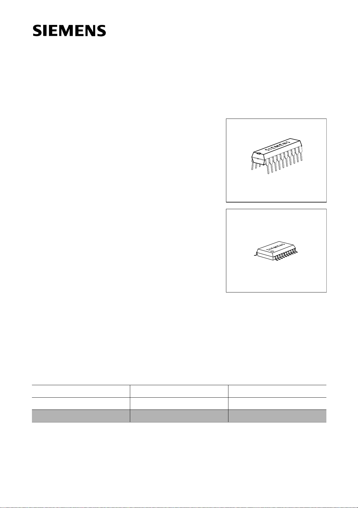
P-DIP-20-5
P-DSO-20-1
PWM Section
– Improved current mode control
– Fast, soft switching totem pole gate drive (1 A)
– Soft-start management
– Trailing edge triggered pulse width modulation
– Topologies of PWM converter are feed forward or flyback
– 50% maximum duty cycle to prevent transformer saturation
f
PWM
= f
PFC
–
Type Ordering Code Package
▼ TDA 16888 Q67000-A9284-X201-K5 P-DIP-20-5
▼
TDA 16888G Q67000-A9310-A702 P-DSO-20-1
▼ New type
Semiconductor Group 1 Data Sheet 1998-05-06
Page 2

TDA 16888
Special Features
– High power factor
–Typical 50µA start-up supply current
– Low quiescent current (15 mA)
– Undervoltage lockout with internal stan d-by operatio n
– Internally synchronized fixed operating frequency ranging from 15 kHz to 200 kHz
– External synchroniz ati on poss ible
– Shutdown of both outputs externally triggerable
– Peak current limitation
– Overvoltage protection
– Average current sensing by noise filtering
1.2 General Remarks
The TDA 16888 comprises the complete control for power factor controlled switched
mode power supplies. Wi th its PFC and PWM sec tion being internal ly synchronized, it
applies for off-line converters with input voltages ranging from 90 V to 270 V.
While the preferred topologies of the PFC preconverter are boos t or flyback, the PWM
section can be designed as forward or flyback converter. In order to achieve minimal line
current gaps the maximum duty cycle of the PFC is about 94%. The maximum duty cycle
of the PWM, however, is limited to 50% to prevent transformer saturation.
Semiconductor Group 2 Data Sheet 1998-05-06
Page 3

TDA 16888
P-DSO-20-1P-DIP-20-5
20
19
18
17
16
15
14
13
12
11
AUX VS
PFC VS
PFC VC
PFC FB
ROSC
PWM RMP
PWM IN
PWM SS
SYNC
REF
CC
1
2
3
4
5
6
7
8
9
10
AEP02461
PFC IAC
V
PFC CC
PFC CS
GND S
PFC CL
GND
PFC OUT
V
PWM OUT PWM CS
PFC IAC
V
REF
PFC CC
PFC CS
GND S
PFC CL
GND
PFC OUT
V
CC
PWM OUT
1
2
3
4
5
6
7
8
9
10
20
19
18
17
16
15
14
13
12
11
AEP02486
AUX VS
PFC VS
PFC VC
PFC FB
ROSC
PWM RMP
PWM IN
PWM SS
SYNC
PWM CS
Figure 1 Pin Configuration (top view)
Semiconductor Group 3 Data Sheet 1998-05-06
Page 4

1.3 Pin Definitions and Functions
Pin No. Symbol Function
1 PFC IAC AC line voltage sensing input
TDA 16888
2
V
REF
7.5 V reference
3 PFC CC PFC current loop compensation
4 PFC CS PFC current sense
5 GND S Ground sensing input
6 PFC CL Sensing i nput for PFC current limitation
7 GND Ground
8 PFC OUT PFC driver output
9
V
CC
Supply voltage
10 PWM OUT PWM driver output
11 PWM CS PWM current sense
12 SYNC Oscillator synchronization inpu t
13 PWM SS PWM soft-start
14 PWM IN PWM output voltage sensing input
15 PWM RMP PWM voltage ramp
16 ROSC Oscillator frequency set-up
17 PFC FB PFC voltage loop feedback
18 PFC VC PFC voltage loop compensation
19 PFC VS PFC output voltage sensing input
20 AUX VS Auxiliary power supply voltage sense
Semiconductor Group 4 Data Sheet 1998-05-06
Page 5
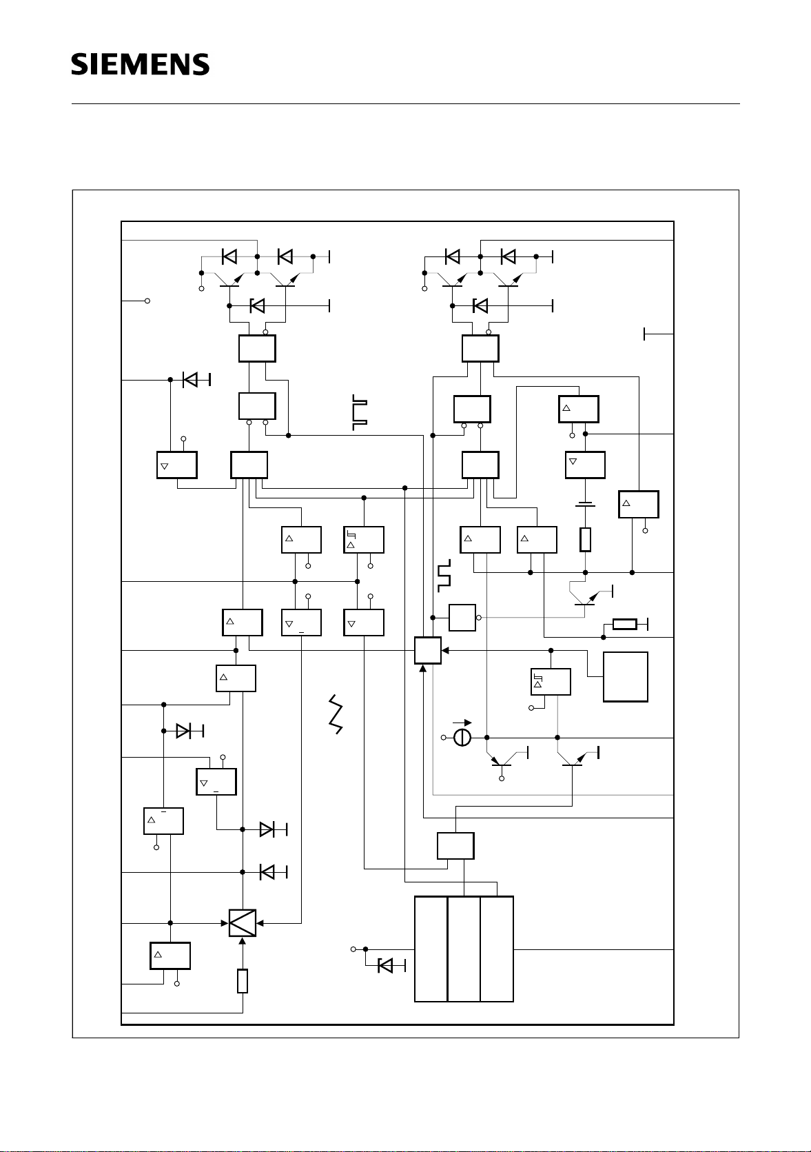
1.4 Block Di a g r am
TDA 16888
PFC
V
PFC
PFC
PFC
OUT
CC
CL
VS
CC
9
6
19
3
C3
10
OUT
PWM
AEB02357
S
V
S
V
Z1
S
V
Z2
7
&
&&
GND
D4
FF1
R
S
FF2
R
S
1 V
+
_
&
C1
C2
+
_
_
+
OTA2
C6
_
+
5.5 V 1 V
_
+
6 V
5.5 V
4 V
+
_
C7
1
C4
C8
_
+
Osc
C9
_
+
1 V
5
OP3
1
V
1.5 V
_
+
C10
Ω
1
R
10 k
3
R
_
+
Ω
100 k
0.4 V
11
15
CS
PWM
RMP
PWM
14
PWM
S
GND
VS
AUX
CSIAC
PFC PFC
FB VC
PFC
PFC
Figure 2
5
20
OTA3
18 4
OP1
17
1 8
+
1.2 V
_
Bias
PWM
Control
13
16
SS IN
PWM
ROSC
D3
OTA1
OP2
+
_
+
5 V
_
A
µ
1
30
Ι
C5
0.45 V
0.4 V
_
+
7.4 V
6 V
12
_
D1 D2
M
Q
3
M
2
M
+
5 V
1
M
Ω
2
R
10 k
S
V
Z3
17.5 V
1
<
_
11 V-14 V
Voltage Reference
Power Management
Undervoltage Lockout
7.5 V (Output Disable)
2
SYNC
REF
V
Semiconductor Group 5 Data Sheet 1998-05-06
Page 6

TDA 16888
2 Functional Description
Power Supply
The TDA 16888 is protecte d again st overvolta ges ty pically above 17.5 V by an internal
V
Zener diod e Z3 at pin 9 (
ESD circuitry.
By means of its power manageme nt the TDA 16888 will switch from in ternal stand-by,
which is characterized by negligible current consumption, to operation mode as soon as
a supply voltage threshold of 14 V at pin 9 (
ringing at switch-over an undervoltage lockout is implemented, which will cause the
power management t o switch from operation mode t o internal stand-by as soon as th e
supply voltage falls bel ow a threshold of 11 V. Therefore, even if the supply voltage wil l
fall below 14 V, operation mode will be maintained as lo ng as the sup ply voltage is well
above 11 V.
) and against electrostatic discharging at any pin by special
CC
V
) is exceeded. To avoid uncontrolled
CC
As soon as the supply v oltage has stabilize d, which is d etermined by the TDA 16888’ s
power management and its soft-start feature at pin 13 (PWM SS), the PWM section will
be enabled by means of its internal bias control.
Protection Circuitry
Both PFC and PWM section are equipped with a fast overvoltage protection (C6)
sensing at pin 19 (PFC VS), which when being activated will immediately shut down both
gate drives. In addition to improve the PFC section’s load regulation it uses a fast but soft
overvoltage protection (OTA2) prior to the one described above, which when being
Q
activated will cause a well controlled throttling of the multiplier output
.
M
In case an undervoltage of the PFC output voltage is detecte d at pin 19 (PFC VS) by
comparator C4 the gate drive of t he PWM section will be s hut down in order to reduce
the load current an d to increase the PFC output voltage. This u ndervoltage shutdown
has to be prior to the undervoltage lockout of the internal power management and
V
therefore has to be bound to a threshold voltage at pin 9 (
) well above 11 V.
CC
In order to prevent the external circuitry from destruction the PFC output PFC OUT
(pin 8) will immediately be switched off by comparator C2, if the voltage at pin 19
(PFC VS) drops to ground caused by a broken wire. In a similar way measures are taken
to handle a broken wire at any other pin in order to ensure a safe operation of the IC and
its adjoining circuitry.
If necessary both outputs, PFC OUT (pin 8) an d PWM OUT (pin 10), can be shutdown
on external request. This is accom plished by shorti ng the external refe rence voltag e at
V
pin 2 (
characteristic, which will cut down the o utput current whe n
) to ground. To protect the external reference, i t is equipped with a foldback
REF
V
(pin 2 ) is shorted (see
REF
Figure 4).
Semiconductor Group 6 Data Sheet 1998-05-06
Page 7

TDA 16888
Both PFC and PWM section are equipped with a peak current limitation, which is realized
by the comparators C3 and C9 sensing at pin 6 (PFC CL) and pin 11 (PWM CS)
respectively. When being activated this current limitation will immediately shut down the
respective gate drive PFC OUT (pin 8) or PWM OUT (pin 10).
Finally each pin is protected against electrostatic discharge.
Oscillator/Synchronization
The PFC and PWM clock signals as well as the PFC voltage ramp are synchronized by
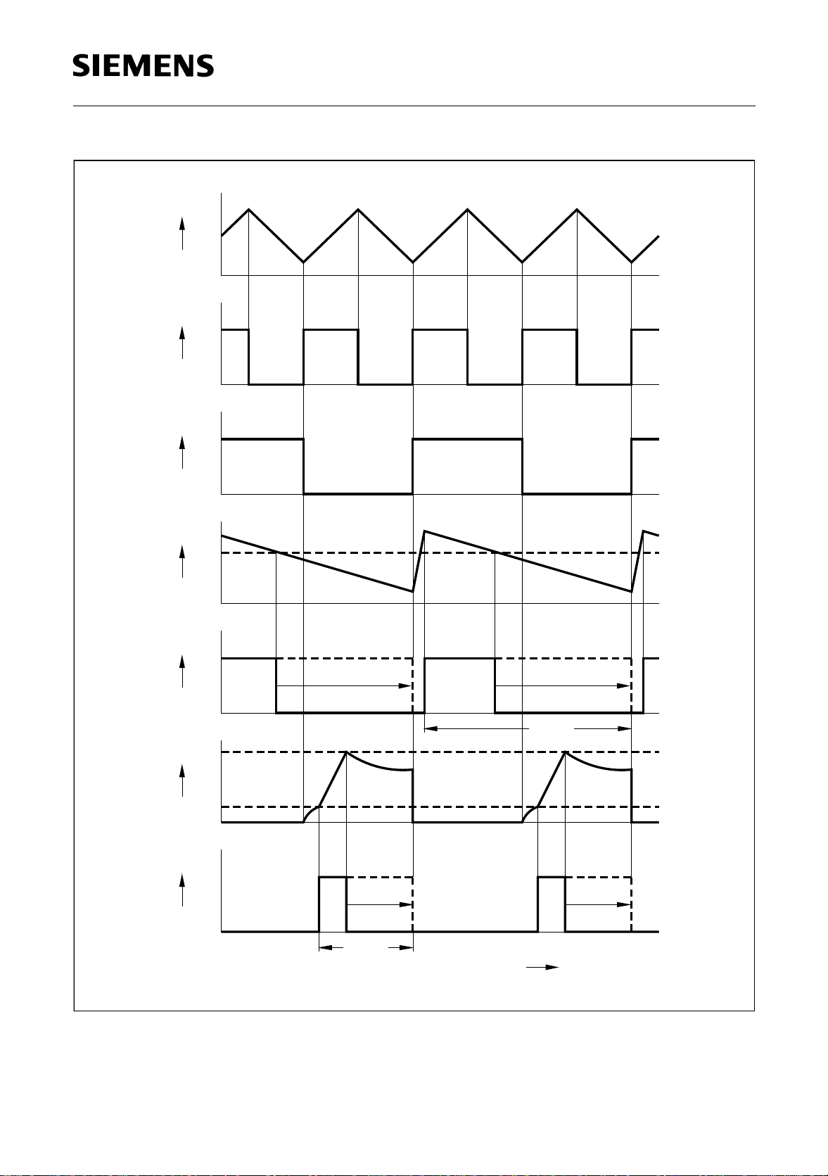
the internal oscillator (see Figure 18). The oscillator’s frequency is set by an external
resistor connected to pin 16 (ROSC) and ground (see Figure 5). The corresponding
capacitor, however, is integrated to guarantee a low current cons umption and a high
resistance against elec tromagnetic interferenc es. In order to ensure superior prec ision
of the clock frequency, the clock signal CLK OSC is derived from a triangular instead of
a saw-tooth signal. Furthermore to provide a clock reference CLK OUT with exactly 50%
duty cycle, the frequency of the oscillator’s clock signal CLK OSC is halved by a D-latch
before being fed into the PFC and PWM section respectively (see Figure 18).
The ramp signal of the PFC section
V
PFC RMP
is composed of a slowly falling and a
steeply rising edge. This ramp has been reversed in contrast to the common practice, in
order to simultaneously allow for current measurement at pin 5 (GND S) and for external
compensation of OP2 by means of pin 5 (GND S) and pin 3 (PFC CC).
The oscillator can be synchronized with an external clock signal supplied at pin 12
(SYNC). However, since the oscilla tor’s frequency is halved before being fed into the
PFC and PWM section, a synchronization frequency being twice the operating frequency
is recommended. As long as th e synchronization signal is H the os cillator’s triangular
V
signal
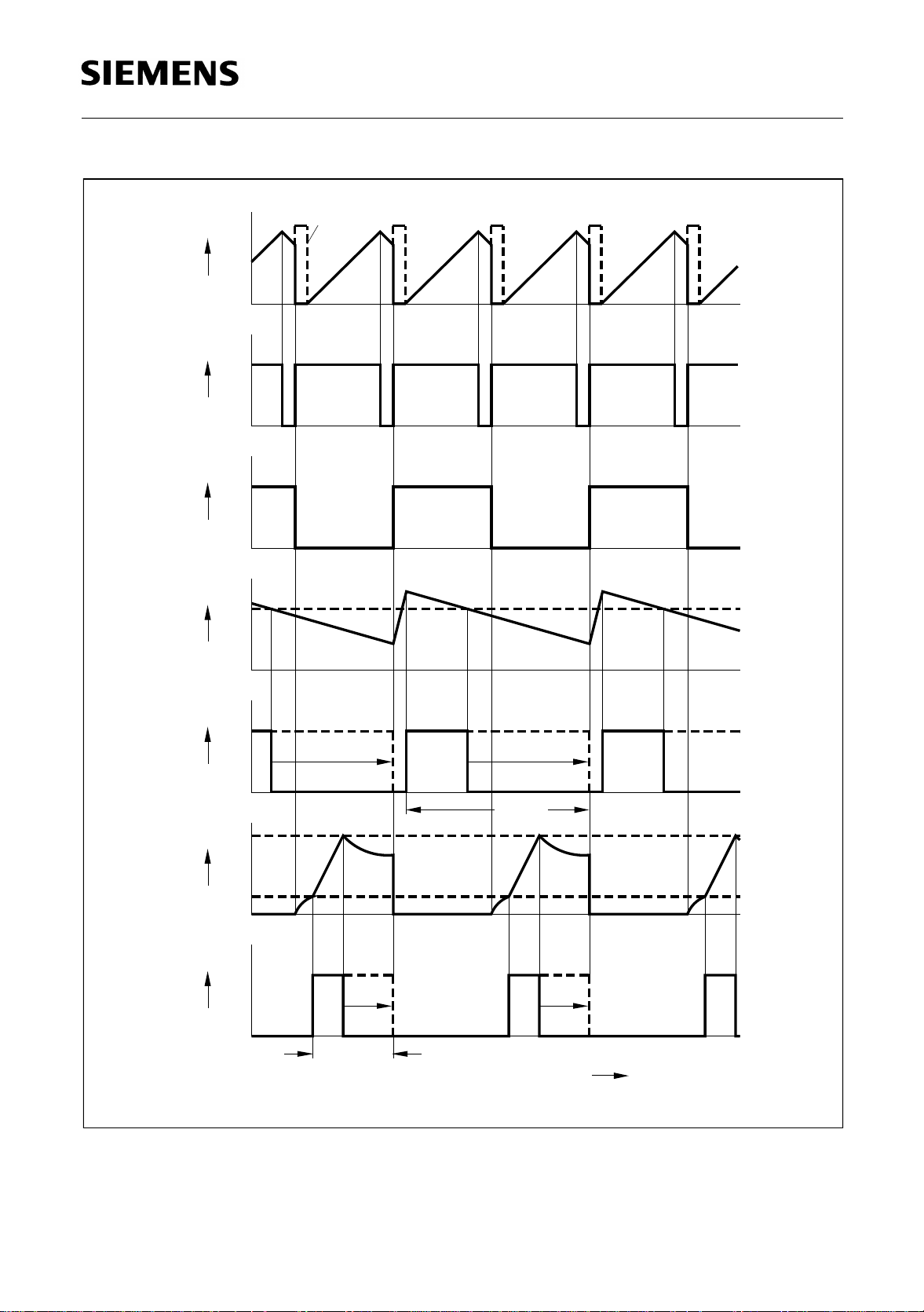
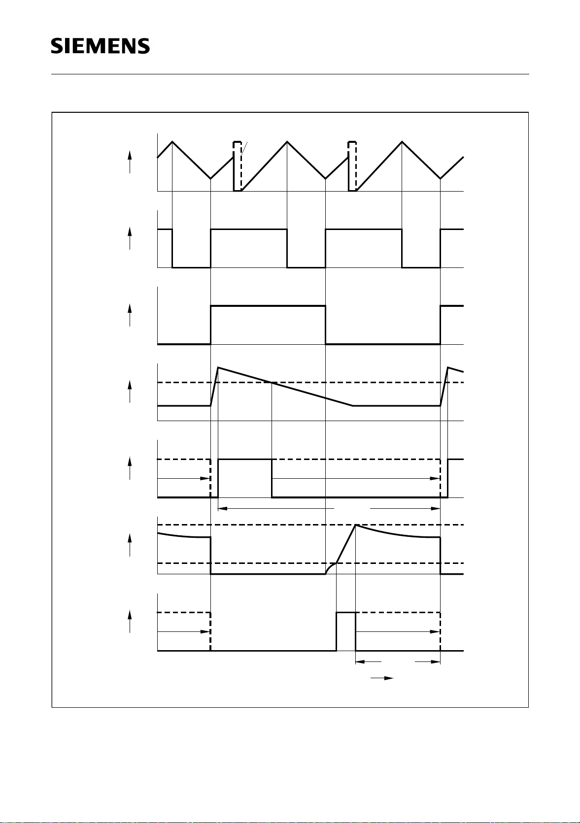
is interrupted and its clock signal CLK OSC is H (see Figure 19 and
OSC
Figure 20). However, as soon as the external clock changes from H to L the oscillator is
released. Correspondingly, by means of an external clock signal supplied at pin 12
f
(SYNC) the oscillator frequency
varied on principle only within the range from 0.66
set by an external resistor at pin 16 (ROSC) can be
OSC
f
OSC
to 2 f
. If the oscillator has to
OSC
be synchronized over a wider freq uency rang e, a synch roni zation by means of the s ink
current at pin 16 (ROSC) has to be preferred to a synchronization by means of pin 12
(SYNC). Anyhow, please note, that pin 12 (SYNC) is not meant to permanently
shutdown both PFC and PWM section. It can be used to halt the oscil lator freezi ng the
prevailing state of both drivers but does not allow to automatically shut th em down. A
V
shutdown can be achieved by shorting pin 2 (
) to ground, instead.
REF
Finally, In order to reduce the overall current consumption under low load conditions, the
oscillator frequency itself is halv ed as long as the voltage at pin 13 (PWM SS) is less
than 0.4 V (disabled PWM section).
Semiconductor Group 7 Data Sheet 1998-05-06
Page 8

TDA 16888
PFC Section
At normal operation the PFC section operates with dual loop control. An inner loop,
which includ es OP2, C 1, FF1 and the PF C’s driv er, cont rols the s hape of the lin e current
by average current control enabling either continuous or discontinuous operation. By the
outer loop, which is supported by OP1, the multiplier, OP2, C1, FF1 and the PFC's driver,
the PFC output voltage is controlled. Furthermore there is a third control loop composed
of OTA1, OP2, C1, FF1 and the PFC’s driver, which allows the PFC section to be
operated as an auxiliary power su pply even when the PWM section is disabled. With
disabled PWM section, however, the PFC section is operated with ha lf of its nominal
operating frequency in order to reduce the overall current consumption.
Based on a pulse-wi dth-m odulation, which is leading edge triggered with respect to the
internal clock reference CLK OUT and which is trailing edge modulated according to the
PFC ramp signal
V
PFC RMP
PFC section is designed fo r a maximum duty cycl e of ca. 94% to achiev e minimal line
current gaps.
and the output voltage of OP2 V
PFC CC
(see Figure 1 8), the
PWM Section
The PWM section is e quipped with improved cu rrent mode con trol containin g effective
slope compensation as well as enhanced spike suppression in contrast to the commonly
used leading edge current blanking. This is achieved by the chain of operational amplifier
V
OP3, voltage source
and the 1st order low pass filter composed of R1 and an external
1
capacitor, which is connected to pin 15 (PWM RMP). For crosstalk suppression between
PFC and PWM section a signal-to-no ise ratio comparable to voltage mode controlled
PWM’s is set by operational amplifier OP3 performing a fivefold amplification of the PWM
load current, which is sense d by an external shunt resistor. In order to simulta neously
perform effective slope compensation and to suppress leading spikes, which are due to
parasitic capacitances bei ng disch arged whenever the power transisto r is switched on,
V
the resulting signal is su bsequently increas ed by the constant volta ge of
and finally
1
fed into the 1st order low pass fi lter. The peak ramp voltage, that in this way can be
V
reached, amounts to ca. 6. 5 V. By combination of voltag e source
and the following
1
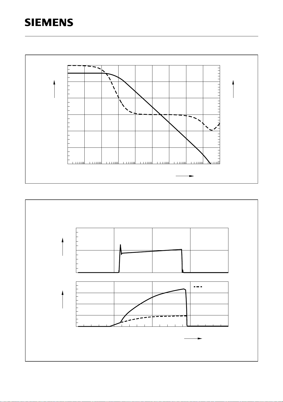
low pass filter a basic ramp (step response) with a leading notch is crea ted, which will
fully compensate a leading spike (see Figure 12) provided, the external capacitor at
pin 15 (PWM RMP) and the external current sensing shunt resistor are scaled properly.
Semiconductor Group 8 Data Sheet 1998-05-06
Page 9

TDA 16888
The pulse-width-modulation of the PWM section is trailing edge modulated according to
the PWM ramp signal
V
PWM RMP
pin 14 (PWM IN) (see Figure 18). In contrast to the PFC secti on, however, the pulsewidth-modulation of the PWM section is trailing edge triggered with respect to the
internal clock reference CLK OUT in order to avoid undesirable electromagnetic
interference of both section s. Moreover the maximu m duty cycl e of the PWM is limited
to 50% to prevent transformer saturation.
By means of the above mentioned improved current mode control a stable pulse-widthmodulation from maximum load down to no lo ad is achi eved. Finally, in case of no load
conditions the PWM section may as well be disabled by shorting pin 13 (PWM SS) to
ground.
at pin 15 (PWM RMP) and the input volta ge V
PWM IN
at
Semiconductor Group 9 Data Sheet 1998-05-06
Page 10

TDA 16888
3 Functional Block Description
Gate Drive
Both PFC and PWM section use fast tot em pole gate drives at pin 8 (PFC OUT) and
pin 10 (PWM OUT) respectively, which are designed to avoid cross conduction currents
and which are equipped with Zener diodes (Z1, Z2) in order to improve the control of the
attached power transistors as well as to protect them against undesirable gate
overvoltages. At voltages below the undervoltage lockout threshold these gate drives are
active low. In order to keep the switching losses of the involved power diodes low and to
minimize electroma gnetic emissions, both gate drives are optimized for s oft switching
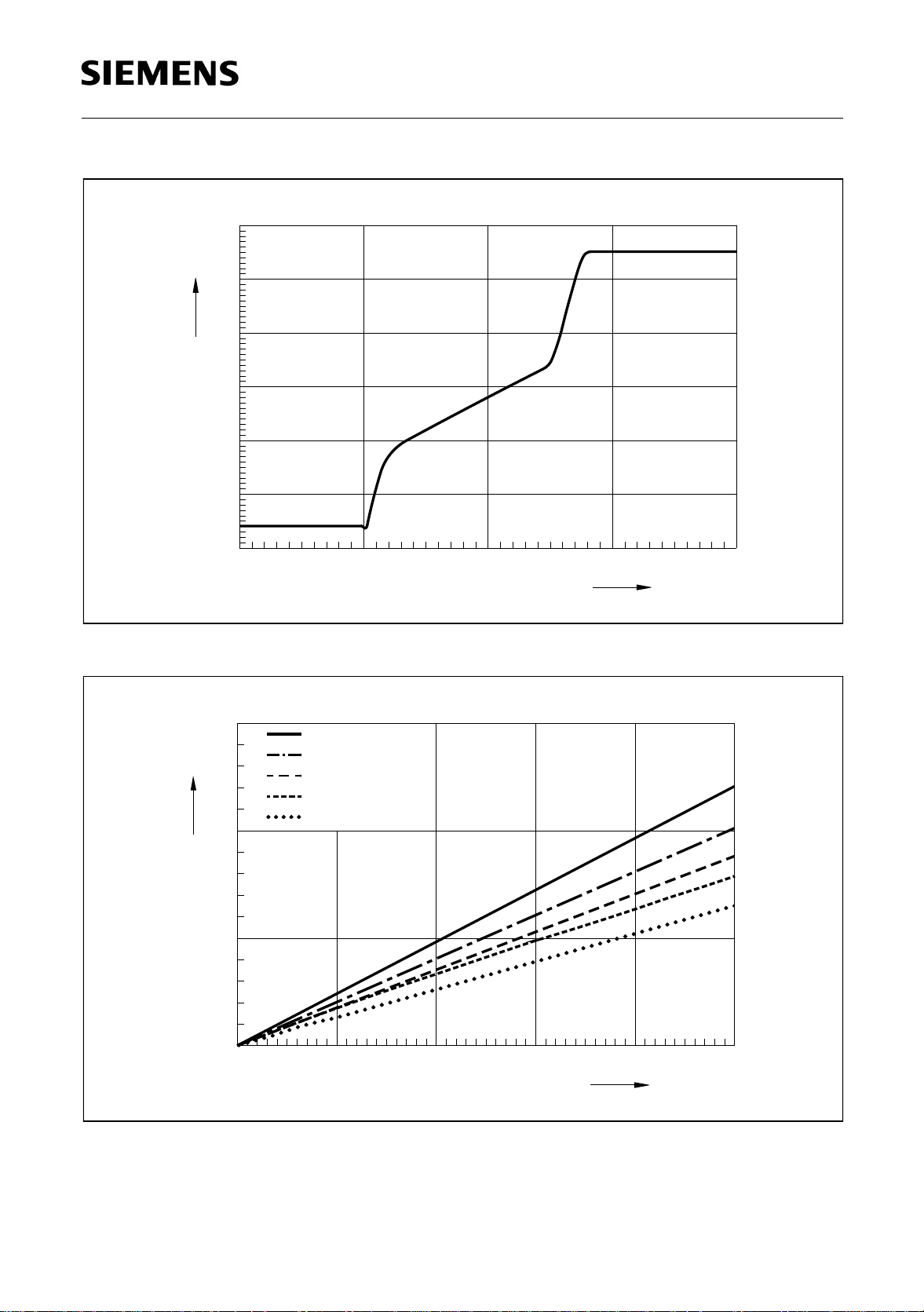
operation. This is achie ved by a novel slope cont rol of the rising edge at each d river’s
output (see Figure 13).
Oscillator
The TDA 16888’s clock signals as well as the PFC voltage ram p are provided by the
internal oscillator. Th e oscillat or’s frequency i s set by a n external resistor connected to
pin 16 (ROSC) and ground (see Figure 5). The correspon ding capacitor, however, is
integrated to guarantee a low current consumption and a high resistance against
electromagnetic interferences. In order to ensure superior precision of the clock
frequency, the clock signal CLK OSC is derived from the minima and maxima of a
triangular instead of a saw-tooth signal (see Figure 18). Furthe rmor e, to pr ovide a cl ock
reference CLK OUT with exactly 50% duty cycle, the freq uency of the os cillator ’s clock
signal CLK OSC is halved by a D-latch before being fed into the PFC and PWM section
respectively.
The ramp signal of the PFC section
V
PFC RMP
is composed of a slowly falling and a
steeply rising edge, the latter of which is triggered by the rising edge of the clock
reference CLK OUT. This ramp has been revers ed in c ontrast to t he common practic e,
in order to simultaneously allow for current measurement at pin 5 (GND S) and for
external compensation of OP2 by means of pin 5 (GND S) and pin 3 (PFC CC). The
slope of the falling edge, which in conjunction with the output of OP2 controls the pulsewidth-modulation of the PFC output signal
V
PFC OUT
, is derived from the current set by the
external resistor at pin 16 (ROSC). In this way a cons tant amplitu de of the ram p signal
(ca. 4.5 V) is ensured. In contrast, the slope of the rising edge, which marks the minimum
blanking interval and therefore li mits the max imum duty c ycle
t
of the PFC output
on,max
signal, is determined by an internal current source.
In contrast to the PFC section the ramp signal of the PWM section is trailing edge
triggered with respect to the internal clock reference CLK OUT to avoid undesirable
electromagnetic interference of both sections. Moreover, the maximum duty cycle of the
PWM is limited by the risi ng edge of the clock reference CLK OUT to 50% to pr event
transformer saturation.
Semiconductor Group 10 Data Sheet 1998-05-06
Page 11

TDA 16888
The oscillator can be synchronized with an external clock signal supplied at pin 12
V
(SYNC). As long as this clock signal is H the oscillator’s triangular signal
interrupted and its clock signal CLK OSC is H (see Figure 19 and Figure 20). However,
as soon as the external clock changes from H to L the oscillator is released.
Correspondingly, by me ans of an external clock signal su pplied at pin 12 (SYNC) the
f
oscillator frequency
principle only within the range from 0.66
set by an extern al resisto r at p in 16 (ROSC) can be varied on
OSC
f
OSC
to 2 f
. Please note, that the slope of the
OSC
falling edge of the PFC ramp is not influenced by the synchronization frequency. Instead
the lower voltage peak is modulated. Consequently, on the one hand at high
synchronization frequencies
f
SYNC
> f
the amplitude of the ramp signal and
OSC
correspondingly its signal-to-noise ratio is decreased (see Figure 19). On the other hand
at low synchronization frequencies
f
SYNC
< f
the lower voltage peak is clamped to the
OSC
minimum ramp voltage (typ. 1.1 V), that at least can be achieved (see Figure 20), which
may cause undefined PFC dut y cycles as th e voltage
V
PFC CC
at pin 3 (PFC CC) drops
below this threshold. However, if the oscillator has to be synchronized over a wide
frequency range, a synch ronizati on by m eans of the sink current a t pin 16 (ROSC) has
to be preferred to a synchronization by means of pin 12 (SYNC).
OSC
is
In order to reduce the overall current consumption under low load conditions, the
oscillator frequency itself is halv ed as long as the voltage at pin 13 (PWM SS) is less
than 0.4 V (disabled PWM section).
Multiplier
I
The multiplier serves to pro vide the c ontrolled current
I
of the sinusoidal input current
R
of the 10 k Ω resistor
, the magnitude of the PFC output voltage VM2 given at pin 18
2
derived from the voltage at pin 1 (PFC IAC) by means
M1
(PFC VC) and the possibility for soft overvoltage protection
Protection Circuitry
). By means of this current the required power factor as well as the
by combination of the shape
QM
V
M3
(see
Chapter
magnitude of the PFC output voltage is ensured. To achieve an excellen t performan ce
V
over a wide range of output po wer and i nput voltage , the input vol tage
is amplified
M2
by an exponential function before being fed into the multiplier (see Figure 8).
Voltage Amplifier OP1
Being part of the outer loop the error amplifier OP1 c ontrols the magnitude of the PFC
output voltage by comparis on of the PFC output voltage me asured at pin 17 (PFC FB)
with an internal reference voltage. The latter is fixed to 5 V in order to achieve immunity
from external noise. To allow fo r individual fe edback the ou tput of OP1 is con nected to
pin 18 (PFC VC).
Semiconductor Group 11 Data Sheet 1998-05-06
Page 12

TDA 16888
Current Amplifier OP2
Being part of the inner loop the error amplifier OP2 controls the shape of the line current
I
by comparison of the controlled current
is achieved by setting the pulse width of the PFC gate drive in conjunction with the
comparator C1. In order to limit the voltage range supplied at pin 4 (PFC CS) and at pin 5
(GND S), clamping diodes D1, D2 and D3 are connected with these pins and ground. To
allow for individual feedback the output of OP2 is connected to pin 3 (PFC CC).
Ramp Amplifier OP3
For crosstalk suppression between PFC and PWM section a signal-to-noise ratio
comparable to voltage mode controlled PWMs is set by operational amplifier OP3
performing a fivefold amplification of the PWM load current, which is sensed by an
external shunt resistor. In order to suppress leading spikes, which are du e to parasitic
capacitances being discharged whenever the power transistor is switched on, the
resulting signal is subsequ ently increased by the constant voltage of
into a 1st order low pass filter. By combination of voltage source
pass filter a step response with a leading notch is created, which will fully compensate a
leading spike (see Figure 12) provided, the external capacitor at pin 15 (PWM RMP)
and the external current sensing shunt resistor are scaled properly.
with the measured average line current. This
QM
V
and finally fed
1
V
and the following low
1
Operational Transconductance Amplifier OTA1
The TDA 16888’s auxiliary power supply mode is controlled by the fast operational
transconductance amplifier OTA1. When under low load or no load conditions a voltage
below 5 V is sensed at pin 20 (AUX VS), it will sta rt to superimpose its output on the
output Q
of the multiplier and in thi s way will replace the error a mplifier OP1 and the
M
multiplier. At normal operat ion, however, when the voltage at pin 20 (AUX VS) is well
above 5 V, this operational transconductance amplifier is disabled.
Operational Transconductance Amplifier OTA2
By means of the operational transconductance amplifier OTA2 sensing at pin 19
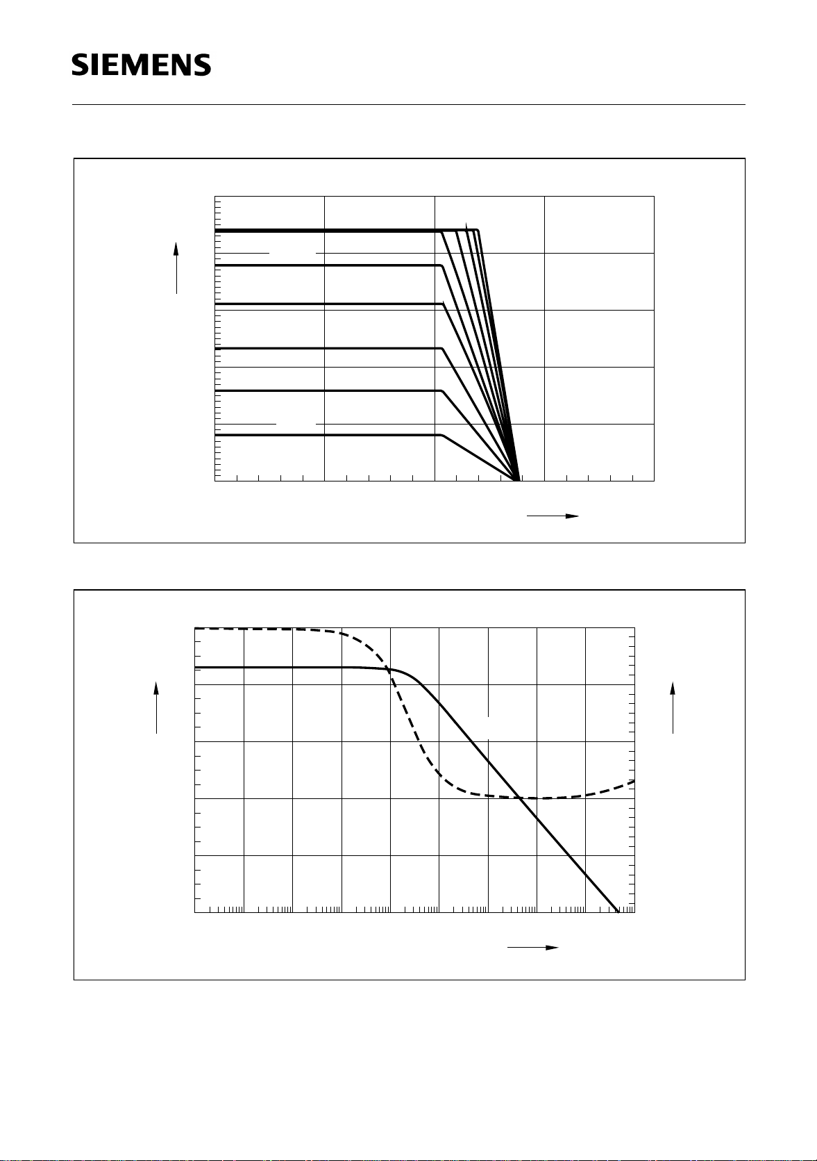
(PFC VS) a f ast but soft overvo ltage protection of t he PFC output voltag e is achieved,
which when being activated (
multiplier output Q
(see Figure 9).
M
V
PFC VS
> 5.5 V) will cause a well controlled throttling of the
Operational Transconductance Amplifier OTA3
In order to achieve offset compensation of error amplifier OP2 under low load conditions,
that will not suffice to start OTA1, the operational transc onductance amplifier OTA3 is
introduced. It will start operation as soon as these conditions are reached, i.e. the voltage
at pin 18 (PFC VC) falls below 1.2 V.
Semiconductor Group 12 Data Sheet 1998-05-06
Page 13

TDA 16888
Comparator C1
The comparator C1 serves to adjust the duty cycle of the PFC gate drive. This is
achieved by comparison of the output voltage of OP2 given at pin 3 (PFC CC) and the
voltage ramp of the oscillator.
Comparator C2
The comparator C2 serves to prevent the external circuitry from destruction by
immediately switching the PFC output PFC OUT (pin 8) off, if the voltage at pin 19
(PFC VS) drops below 1 V due to a broken wire.
Comparator C3
By means of this extremely fast comparator sensing at pin 6 (PFC CL) peak current
limitation is realized. When being activated (
V
PFC CL
the gate drive of the PFC section (pin 8, PFC OUT). In order to protect C3 against
undervoltages at pin 6 (PFC CL) due to large inrush currents, this pin is equi pped with
an additional clamping diode D4.
< 1 V) it will immediately shut down
Comparator C4
This comparator along with the TDA 16888’s power man agement serves to reset the
PWM section’s soft start at pin 13 (PWM SS). C4 becomes active as soon as an
undervoltage (
V
PFC VS
< 4 V) of the PFC output voltage is sensed at pin 19 (PFC VS).
Comparator C5
Based on the status of the PWM section’s soft start at pin 13 (PWM SS), the comparator
C5 controls the bias of the entire PWM section. In this way the PWM section is switched
off giving a very low quiescent current, until its soft start is released.
Comparator C6
Overvoltage protection of the PWM section’s input voltage sensed at pin 19 (PFC VS) is
realized by comparator C6, which when being activated will immediately shut down both
gate drives PFC OUT (pin 8) and PWM OUT (pin 10).
Comparator C7
This comparator sensing at pin 13 (PWM SS) and at pin 15 (PWM RMP) controls the
pulse width modulation of the PWM section du ring the soft start. This is done right after
the PWM section is biased by comparator C5.
Semiconductor Group 13 Data Sheet 1998-05-06
Page 14

TDA 16888
Comparator C8
The control of the pulse width modulation of the PWM section is taken over by
comparator C8 as soon as the soft start is fini shed. This is achieved by comparison of
the PWM output voltage at pin 14 (PWM IN) and the PWM voltage ramp at pin 15
(PWM RMP).
Comparator C9
By means of this extremely fast com parator sensing at pin 11 (PWM CS ) peak current
limitation is realized. When being activated (
V
PWM CS
the gate drive of the PWM section (PWM OUT).
Comparator C10
By means of the threshold of 0.4 V the comparator C10 allows the PWM duty cycle to be
continuously controlled from 0 to 50%. As long as the ramp voltage at pin 15
(PWM RMP) is below this threshold the gate drive of the PWM section (pin 10,
PWM OUT) is turned off.
> 1 V) it will immed iately sh ut down
Semiconductor Group 14 Data Sheet 1998-05-06
Page 15
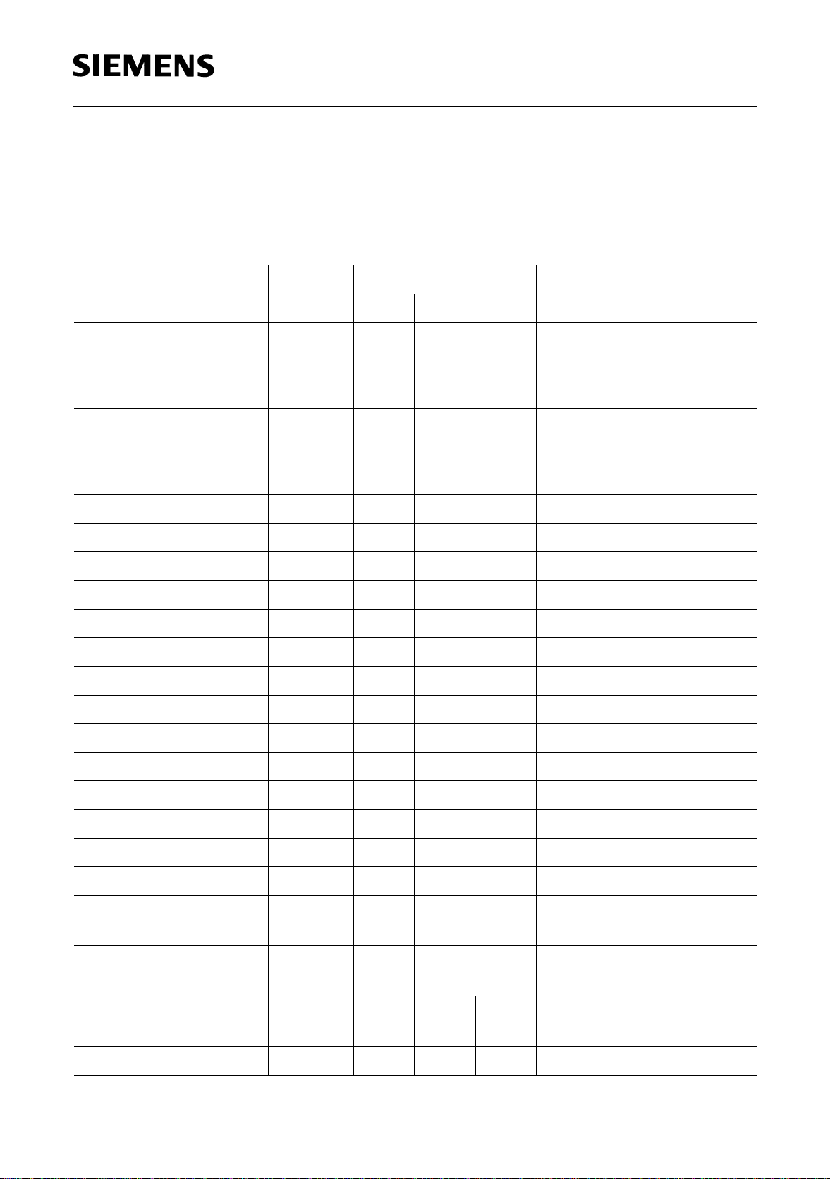
4 Electrical Characteristics
4.1 Absolute Maximum Ratings
T
= – 25 to 85 °C
A
Parameter# Symbol Limit Values Unit Remarks
min. max.
V
supply voltage V
CC
S
–0.3 V
Z3
V VZ3= Zener voltage of Z3
TDA 16888
Zener current of Z3
V
voltage V
REF
ROSC voltage V
SYNC voltage V
PFC FB volt age
PFC IAC voltage
AUX VS voltage
PFC VS voltage
PFC CL volt age
PWM SS voltage
PWM IN voltage V
PWM RMP voltage
PWM CS voltage V
PFC VC voltage
PFC VC current
I
Z3
VREF
ROSC
SYNC
V
PFC FB
V
PFC IAC
V
AUX VS
V
PFC VS
V
PFC CL
V
PWM SS
PWM IN
V
PWM RMP
PWM CS
V
PFC VC
I
PFC VC
–50mA–
– 0.3 8 V V
– 0.3 8 V V
VREF
ROSC
< V
– 0.3 8 V –
– 0.3 8 V –
– 0.3 15 V –
– 0.3 8 V –
– 0.3 8 V |I
PFC VS
– 0.3 3 V –
– 0.3 8 V V
PWM SS
– 0.3 8 V –
– 0.3 8 V V
PWM RMP
– 0.3 3 V –
– 0.3 8 V –
– 20 20 mA –
S
< V
S
|<1mA
< V
VREF
< V
VREF
PFC CS current
GND S current
PFC CC voltage
PFC CC current
PFC/PWM OUT DC
I
PFC CS
I
GND S
V
PFC CC
I
PFC CC
I
OUT
– 5 5 mA –
– 5 5 mA –
– 0.3 8 V –
– 20 20 mA –
– 100 100 mA –
current
PFC/PWM OUT peak
I
OUT
–200mAV
OUT
=High
clamping current
PFC/PWM OUT peak
I
OUT
–500 – mA V
OUT
= Low
clamping current
Junction temperature
Semiconductor Group 15 Data Sheet 1998-05-06
T
J
–40 150 °C–
Page 16
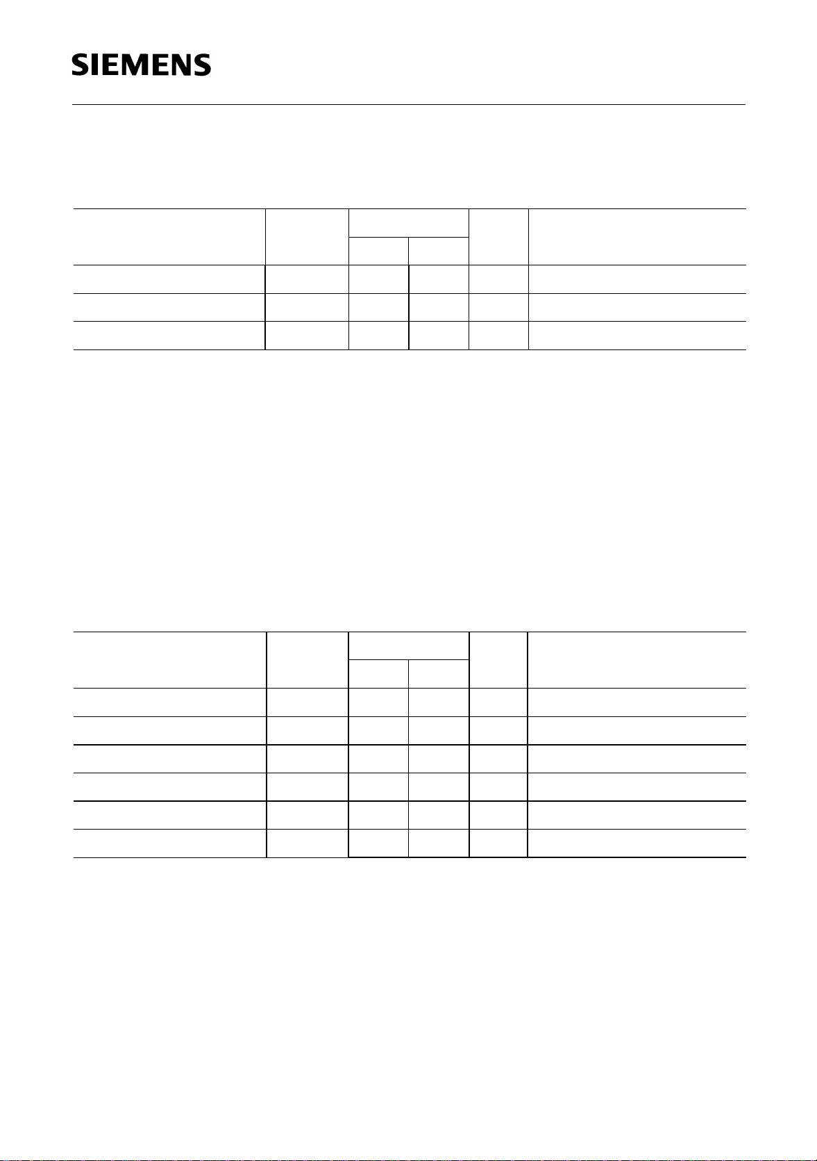
4.1 Absolute Maximum Ratings (cont’d)
T
= – 25 to 85 °C
A
Parameter# Symbol Limit Values Unit Remarks
min. max.
TDA 16888
Storage temperature T
Thermal resistance
Thermal resistance
R
R
S
thJA
thJA
–65 150 °C–
– 60 K/W P-DIP-20-5
–70K/WP-DSO-20-1
Note: Absolute maximum ratings are defined as ratings, which when being exceeded
may lead to destruction of t he integra ted circu it. To avoi d destruction make su re,
that for any pin except for pins PFC OUT and PWM OUT the currents caused by
transient processes stay well below 100 mA. For the same reason make sure, that
V
any capacitor that will be connected to pin 9 (
) is discharged before
CC
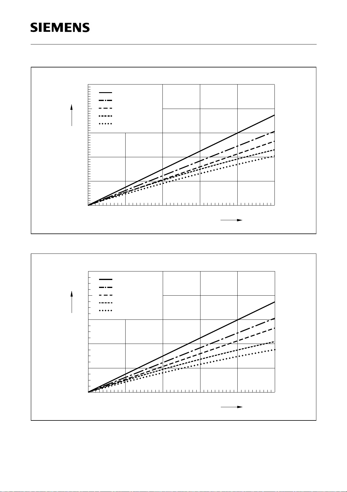
assembling the application circuit. In order to characterize the gate driver’s output
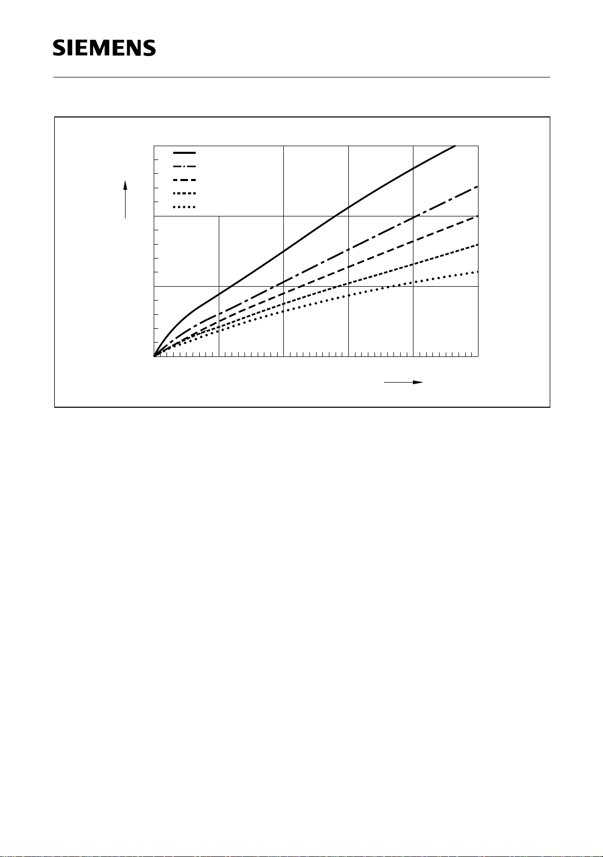
performance Figure 14, Figure 15, Figure 16 and Figure 17 are provided,
instead of referring just to a single parameter like the maximum gate charge or the
maximum output energy.
4.2 Operating Range
Parameter Symbol Limit Values Unit Remarks
min. max.
V
supply voltage V
CC
Zener current
PFC/PWM OUT current I
PFC IAC input current
PFC/PWM frequency
Junction temperature
S
I
Z3
OUT
I
PFC IAC
f
OUT
T
J
0 V
Z3
V VZ3 = Zener voltage of Z3
0 50 mA Limited by T
–1 1.5 A –
01mA–
15 200 kHz –
–25 125 °C–
J,max
Note: Within the operating range the IC operates as described in the functional
description. In order to characterize the gate driver’s output performance
Figure 14, Figure 15, Figure 16 and Figure 17 are provided, instead of referring
just to a single parame ter like the m aximum ga te charge or the ma ximum outp ut
energy.
Semiconductor Group 16 Data Sheet 1998-05-06
Page 17

TDA 16888
4.3 Characteristics
Supply Section
Parameter Symbol Limit Values Unit Test Condition
min. typ. max.
Zener voltage
Zener current
1)
V
I
Z3
Z3
16.0 17.5 19.0 V IZ3=30mA
––500µA VS≤ 15.5 V
2)
Quiescent supply
I
S
––12mAV
current
––15mA
Supply current
1)
See Figure 3
2)
Design characteristics (not me ant fo r production testing)
I
S
––40mAV
PWM SS
R
ROSC
C
L
=0V
=51kΩ
=0V
PFC enabled
PWM disabled
V
PWM SS
R
ROSC
C
L
=6V
=51kΩ
=0F
PFC enabled
PWM enabled
PWM SS
R
ROSC
C
L
=6V
=51kΩ
=4.7nF
PFC enabled
PWM enabled
Note: The electrical characteri stics involve the spread of values guara nteed within the
T
specified supply voltage and ambient temperature range
from – 25°C to 85°C
A
Typical values represent the median values, which are related to production
V
processes. If not otherwise stated, a supply voltage of
Semiconductor Group 17 Data Sheet 1998-05-06
=15V is assumed.
S
Page 18

TDA 16888
Undervoltage Lockout
Parameter Symbol Limit Values Unit Test Condition
min. typ. max.
Power up,
V
S,UP
13.0 14.0 14.5 V –
rising voltage
threshold
Power down,
1)
V
S,DWN
10.5 11.0 11.5 V –
falling voltage
threshold
Power up,
threshold current
1)
I
S,UP
– 23 100 µA VS= V
V
PFC CL
–0.1V
S,UP
<0.3V
Stand-by mode
1)
See Figure 3
2)
To ensure the voltage fallback of pin PFC CL is dis abled.
Internal Voltage Reference
Parameter Symbol Limit Values Unit Test Condition
min. typ. max.
Trimmed reference
voltage
V
REF
4.9 5.0 5.1 V Measured at
pin PFC VC
2)
Line regulation ∆
V
REF
––40mV∆VS=3V
Semiconductor Group 18 Data Sheet 1998-05-06
Page 19

TDA 16888
External Voltage Reference
Parameter Symbol Limit Values Unit Test Condition
min. typ. max.
Buffered output voltage
Line regulation ∆
Load regulation ∆
Maximum output
current
Short circuit current
1)
1)
Shutdown hysteresis,
V
VREF
V
V
I
VREF
I
VREF
V
VREF
VREF
VREF
7.2 7.5 7.8 V –3mA≤ I
––50mV∆VS=3V
040100mV∆I
–10–6–4mAV
––2–mAV
–6.6–V–
rising voltage threshold
Shutdown hysteresis,
V
VREF
–6.2–V
falling voltage threshold
Shutdown delay
1)
See Figure 4
2)
Design characteristics (not me ant fo r production testing)
3)
Transient reference value
t
d,VREF
–500–nsV
VREF
VREF
VREF
–
VREF
V
PFC OUT
V
PWM OUT
VREF
=2mA
=6.5V
=0V
=5V
2)3)
=3V
=3V
≤ 0
2)3)
2)3)
Oscillator
Parameter Symbol Limit Values Unit Test Condition
min. typ. max.
1)
PFC/PWM frequency
PFC/PWM frequency
1)
PFC/PWM frequency,
line regulation
Maximum ramp voltage
Minimum ramp voltage
SYNC, low level voltage
SYNC, high level voltage
SYNC, input current
1)
See Figure 5
f
OUT50
f
OUT100
f
∆
OUT
V
PFC RMP
V
PFC RMP
V
SYNC
V
SYNC
I
SYNC
43 50 57 kHz R
87 100 113 kHz R
ROSC
ROSC
=110kΩ
=51kΩ
––1%∆VS=3V
R
ROSC
=51kΩ
5.0 5.4 5.6 V –
0.8 1.1 1.4 V –
––0.4V
3.5 – V
VREF
V–
––20µA V
– – 150 µA
–
V
SYNC
SYNC
<0.4V
=3.5V
Semiconductor Group 19 Data Sheet 1998-05-06
Page 20

TDA 16888
PFC Section
Parameter Symbol Limit Values Unit Test Condition
min. typ. max.
Max duty cycle
1)
D
on,PFC
91 94 98 % V
R
C
PFC OUT
=51kΩ
ROSC
=4.7nF
L
=2V
3)
Multiplier throttling
(OTA2), threshold
voltage
2)
Overvoltage protection
(C6), rising voltage
threshold
Overvoltage protection
(C6), falling voltage
threshold
Overvoltage protection
(C6), turn-off delay
Broken wire detection
(C2), threshold voltage
Voltage sense, input
current
Current limitation (C3),
threshold voltage
V
PFC VS
V
PFC VS
V
PFC VS
t
d,OV
V
PFC VS
I
PFC VS
V
PFC CL
5.25.55.8V 0.9I
I
PFC IAC
V
PFC VC
OTA1 disabled
5.86 6.2V –
5.35.55.7V –
–2–µs V
PFC VS
V
PFC OUT
0.93 1 1.07 V –
0.2 0.45 0.7 µA V
PFC VS
0.93 1 1.07 V –
PFC CS
= 100 µA
=6V
=6.5V
=3V
=1V
3)4)
3)4)
Current limitation (C3),
I
PFC CL
1–10µA V
PFC CL
=1V
input current
Current limitation (C3,
V
PFC CL
– 0.9 – – 0.1 V I
PFC CL
=–500µA
D4), clamping voltage
Current limitation (C3),
t
d,CL
turn-off delay
1)
See Figure 6
2)
See Figure 9
3)
Transient reference value
4)
Design characteristics (not meant for production testing)
Semiconductor Group 20 Data Sheet 1998-05-06
30 – 150 ns V
V
C
PFC CL
PFC OUT
=4.7nF
L
=0.75V
=3V
3)
3)
Page 21

TDA 16888
Multiplier
Parameter Symbol Limit Values Unit Test Condition
min. typ. max.
Input current
Input voltage
Exponential function,
threshold voltage
Maximum output current I
Output current
3)
I
PFC IAC
V
PFC VC
V
PFC VC
PFC CS
I
PFC CS
0 –1mA–
0–6.7V–
–1.1–V
1)2)
– 320 – 420 – 550 µA OTA1 disabled
– – 100 – 500 nA I
PFC IAC
V
PFC VC
=0A
=2V
OTA1 disabled
–– 1.2–µA
I
PFC IAC
V
PFC VC
=25µA
=2V
OTA1 disabled
–– 10–µA
I
PFC IAC
V
PFC VC
=25µA
=4V
OTA1 disabled
–– 40–µA
I
PFC IAC
V
PFC VC
=100µA
= 4 V
OTA1 disabled
–– 150–µA
I
PFC IAC
V
PFC VC
=400µA
=4V
OTA1 disabled
–– 170–µA
I
PFC IAC
V
PFC VC
=100µA
=6V
OTA1 disabled
1)
Design characteristics (not me ant fo r production testing)
2)
For input voltages below this threshold the multiplier output current remains constant. For input voltages above
this threshold the output rises exponentially (see Figure 8).
3)
See Figure 7
Semiconductor Group 21 Data Sheet 1998-05-06
Page 22
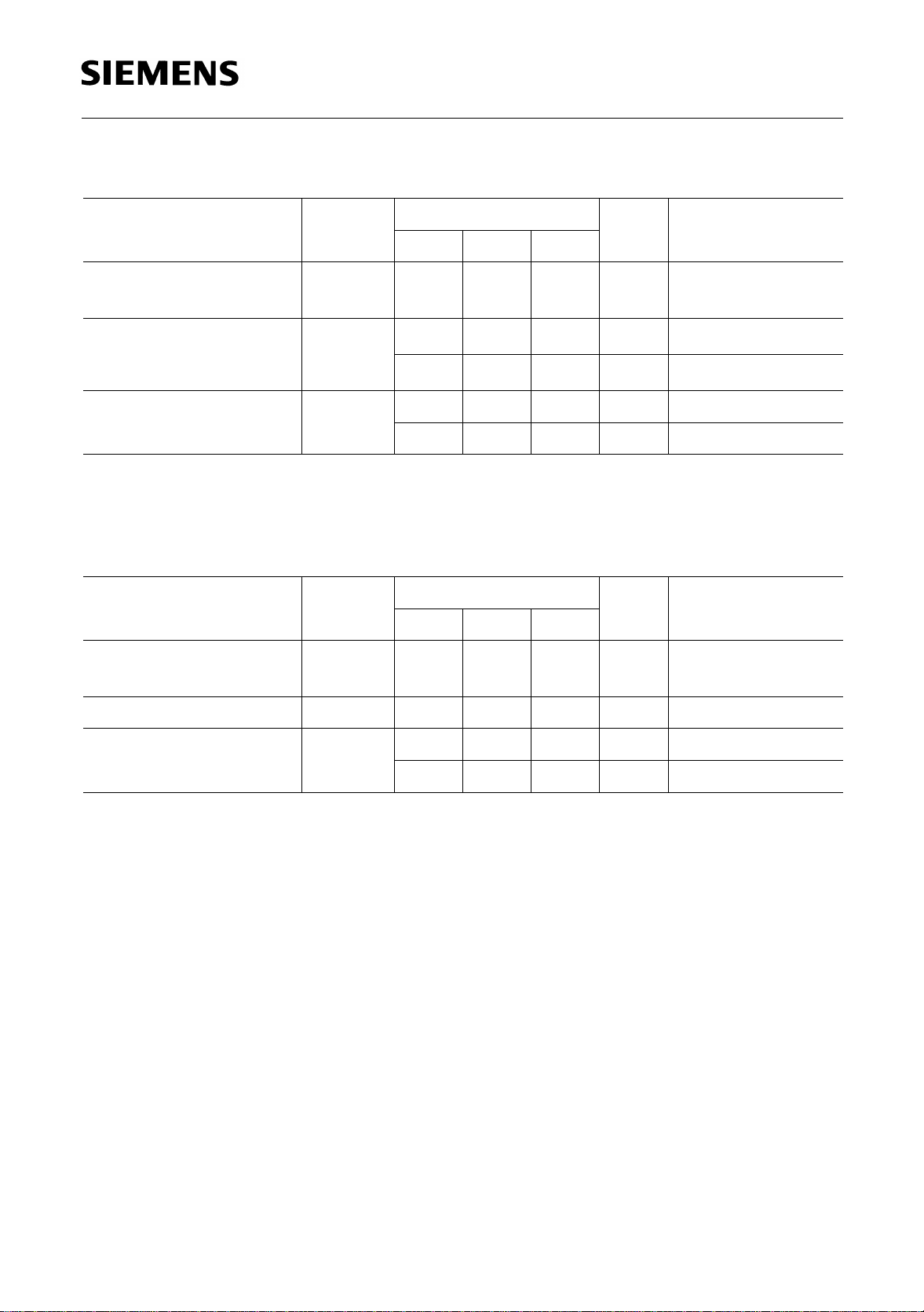
TDA 16888
Operational Transconductance Amplifier (OTA1)
Parameter Symbol Limit Values Unit Test Condition
min. typ. max.
Auxiliary power supply,
threshold voltage
1)
Input current
Output current
1)
For input voltages below this threshold the output current is linearly increasing until at ca. 4.8 V the maximum
output current is reached.
V
AUX VS
I
AUX VS
I
PFC CS
4.8 5.0 5.2 V I
–
–20 –
–15µA
–
µA
–0–µA V
–– 30–µA V
PFC CS
=–1µA
Multiplier disabled
V
AUX VS
V
AUX VS
AUX VS
AUX VS
>5.2V
<4.8V
>5.2V
<4.8V
Operational Transconductance Amplifier (OTA3)
Parameter Symbol Limit Values Unit Test Condition
min. typ. max.
Offset compensation,
V
PFC VC
1.1 1.2 – V –
threshold voltage
Input current
I
PFC VC
– 1 – – µA
1)
1)
Output current I
GND S
–0–µA V
––10–µA
1)
Design characteristics (not meant for production testing)
PFC VC
V
PFC VC
>1.2V
<1.1V
Semiconductor Group 22 Data Sheet 1998-05-06
Page 23

TDA 16888
Voltage Amplifier (OP1)
Parameter Symbol Limit Values Unit Test Condition
min. typ. max.
Offset voltage
V
Off
–4 – 4 mV
1)
Input current I
Open loop gain
Input voltage range V
Voltage sense,
PFC FB
A
PFC VC
PFC FB
V
PFC FB
–1 – 1 µA V
–85–dB
0–6V–
4.9 5 5.1 V –
threshold voltage
Output, maximum
V
PFC VC
6.3 – V
voltage
Output, minimum
V
PFC VC
0.5 – 1.1 V I
voltage
Output, short circuit
I
PFC VC
––10–mAV
source current
Output, short circuit sink
I
PFC VC
–10–mAV
current
1)
Guaranteed by wafer test
2)
Design characteristics (not me ant fo r production testing)
VREF
V I
PFC FB
2)
PFC VC
PFC VC
PFC VC
V
PFC FB
PFC VC
V
PFC FB
=4V
=–500µA
=500µA
=0V
=4.9V
=6.4V
=5.1V
Semiconductor Group 23 Data Sheet 1998-05-06
Page 24

TDA 16888
Current Amplifier (OP2)
Parameter Symbol Limit Values Unit Test Condition
min. typ. max.
Offset voltage
Input current
Open loop gain
Gain bandwidth product
Phase margin
Common mode voltage
range
Clamped input voltage,
upper threshold
(D2, D3)
Clamped input voltage,
lower threshold (D1)
Output, maximum
voltage
V
Off
I
PFC CS
I
GND S
A
PFC CC
f
T
ϕ
V
CMVR
V
PFC CS
V
GND S
V
PFC CS
V
PFC CC
–5 –1 3 mV –
– 500 – 500 nA –
–110–dB–
–2.5–MHz
–60–°
–0.2 – 0.5 V
0.4 – 1.0 V I
1)
1)
1)
PFC CS
I
GND S
Multiplier, OTA1
and OTA3 disabled
–0.9 – –0.1 V I
PFC CS
Multiplier and OTA1
disabled
6.3 – V
VREF
V I
PFC CC
=500µA
= 500 µA
=–500µA
= – 500 µA
Output, minimum
V
PFC CC
0.5 – 1.1 V I
voltage
Output, short circuit
I
PFC CC
––10–mAV
source current
Output, short circuit sink
I
PFC CC
–10–mAV
current
1)
Design characteristics (not meant for production testing)
PFC CC
PFC CC
V
PFC CS
V
GND S
PFC CC
V
PFC CS
V
GND S
=500µA
=0V
=0V
=0.5V
=6.5V
=0.5V
=0V
Semiconductor Group 24 Data Sheet 1998-05-06
Page 25

TDA 16888
PWM Section
Parameter Symbol Limit Values Unit Test Condition
min. typ. max.
Undervoltage protection (C4),
threshold voltage
Bias control (C5),
rising voltage threshold
Bias control (C5),
falling voltage threshold
I
Softstart (
),
1
charging current
Softstart, maximum voltage
Input voltage
PWM IN – GND resistance
Ramp (OP3), voltage gain
Ramp (C10), pulse start
threshold voltage
Ramp, maximum voltage
V
Ramp (
), voltage offset V
1
V
PFC VS
V
BC,Th
V
BC,Th
I
I1
V
PWM SS
V
PWM IN
R
3
A
OP3
V
RMP
V
RMP
V1
3.8 4.0 4.2 V –
–0.45–V–
–0.4–V–
20 30 40 µA–
–6.7–V–
0.4 – 7.4 V –
75 100 150 kΩ –
–5–V/V–
0.36 0.4 0.5 V –
–6.5–V–
–1.5–V–
R
Ramp (
),
1
output impedance
Maximum duty cycle
Current sense (C9),
voltage threshold
Current sense (C9),
overload turn-off delay
1)
Transient reference value
Z
RMP
D
on,PWM
V
CS,Th
t
d,CS
–10–kΩ –
41 – 50 % V
R
C
0.9 1.0 1.1 V –
30 – 250 ns V
V
C
PWM OUT
=51kΩ
ROSC
=4.7nF
L
PWM CS
PWM OUT
=4.7nF
L
1)
=2V
=1.25V
1)
=3V
1)
Semiconductor Group 25 Data Sheet 1998-05-06
Page 26

TDA 16888
Gate Drive (PWM and PFC Section)
Parameter Symbol Limit Values Unit Test Condition
min. typ. max.
Output, minimum
voltage
Output, maximum
voltage
Rise time
1)
Fall time
Output current, rising
3)
edge
Output current, falling
3)
edge
V
V
t
r
t
f
I
OUT
I
OUT
OUT
OUT
––1.2VV
––1.5V
–0.8–V
–1.62.0V
–0.2 0.2 – V
=5V
S
I
=5mA
OUT
V
=5V
S
I
=20mA
OUT
I
=0A
OUT
I
=50mA
OUT
I
=–50mA
OUT
10 11 12 V VS=16V
t
=10µs
H
C
=4.7nF
L
V
10.0 10.5 – V
8.8 – – V
–150–nsV
–100–ns
–30–nsV
–40–ns
=12V
S
t
=10µs
H
C
=4.7nF
L
V
= V
S
t
=10µs
H
C
=4.7nF
L
=2V…8V
OUT
C
=4.7nF
L
V
=3V…6V
OUT
C
=4.7nF
L
=9V…3V
OUT
C
=4.7nF
L
V
=9V…2V
OUT
C
=4.7nF
L
S,DWN
–1 – – A CL=4.7nF
––1.5ACL=4.7nF
+0.2V
2)
2)
2)
2)
4)
4)
1)
See Figure 13
2)
Transient reference value
3)
The gate driver’s output performance is characterized in Figure 14, Figure 15, Figure 16 and Figure 17.
4)
Design characteristics (not meant for production testing)
Semiconductor Group 26 Data Sheet 1998-05-06
Page 27
TDA 16888
Note: If not otherwise stated the figures shown in this section represent typical
performance characteristics.
AED02462
Ι
VCC
Ι
S
Ι
S, UP
V
S, DWN
V
S, UP Z3
V
V
VCC
Figure 3 Undervoltage Lockout Hysteresis and Zener Diode Overvoltage
Protection
AED02463
Ι
VREF
-8
mA
-7
-6
-5
-4
-3
-2
-1
0
V
VREF
V
0
1 2 3 4 5 6 7 8
Figure 4 Foldback Characteristic of Pin 2 (
V
REF
)
Semiconductor Group 27 Data Sheet 1998-05-06
Page 28
TDA 16888
400
kHz
f
OUT
100
10
10
Figure 5 PFC/PWM Frequency
100
R
OSC
AED02464
500
kΩ
100
%
D
on, PFC, max
95
90
85
80
0
100 200 300 400
Figure 6 Maximum PFC Duty Cycle
R
AED02465
kΩ
OSC
Semiconductor Group 28 Data Sheet 1998-05-06
Page 29
TDA 16888
500
µ
Ι
PFC CCS
A
V
PFC VC
= 7 V
400
300
200
100
0
0
0.2 0.4 0.6 0.8 1
Figure 7 Multiplier Linearity
4 V5 V6 V
3 V
2 V
Ι
PFC IAC
AED02466
mA
500
µ
A
Ι
PFC CCS
400
Ι
PFC IAC
300
200
100
0
0
123 4 5 6 7V
Figure 8 Multiplier Dynamic
AED02356
µ
A= 800
A400
µ
A200
µ
A100
µ
A50
µ
A25
µ
V
PFC VC
Semiconductor Group 29 Data Sheet 1998-05-06
Page 30
TDA 16888
500
µ
A
Ι
PFC CCS
400
Ι
PFC IAC
µ
A> 300
A250
µ
A200
µ
300
A150
µ
200
A100
µ
A50
100
µ
0
5.0
5.25 5.5 5.75 6.0V
Figure 9 Multiplier Throttling by OTA2
V
PFC VC
= 6 V
V
PFC VS
AED02467
100
AED02468
0
dB deg
A
PFC VC
80
60
40
20
0
10
10
A
PFC VC
3
10
4
10
5
10
6
10
Hz
φ
-2
10
-1
10
0
10
1
10
2
φ
-30
-60
-90
-120
-150
7
Frequency
Figure 10 Open Loop Gain and Phase Characteristic of Voltage Amplifier OP1
Semiconductor Group 30 Data Sheet 1998-05-06
Page 31
TDA 16888
AED02469
6
10
Hz
10
0
deg
-30
-60
-90
-120
-150
-180
7
φ
A
PFC CC
120
dB
100
80
60
40
20
0
10
10
A
PFC CC
2
10
3
10
4
10
5
φ
-2
10
-1
10
0
10
1
Frequency
Figure 11 Open Loop Gain and Phase Characteristic of Current Amplifier OP2
V
PWM CS
V
V
PWM RMP
V
1
/2
1
AED02470
0
V
4
1
V
3
1
V
2
1
V
1
V
PWMCS
= 0
0
0
T/2 T
Time
Figure 12 PWM Ramp Composition Scheme
Semiconductor Group 31 Data Sheet 1998-05-06
Page 32
TDA 16888
12
V
V
PFC OUT
10
8
6
4
2
0
0
0.1 0.2 0.3 0.4
Figure 13 Rising Edge of Driver Output
Time
AED02471
µ
s
150
mW
P
D
100
R
= 0
Ω
L
R
= 1
Ω
L
R
= 2
Ω
L
R
= 5
Ω
L
R
= 10
Ω
L
50
0
0
10 20 30 40 50nF
Figure 14 Power Dissipation of Single Gate Driver at
f
OUT
AED02542
= 15 kHz
f
OUT
= 0.194 W
P
D0
C
L
=15kHz
Semiconductor Group 32 Data Sheet 1998-05-06
Page 33
TDA 16888
500
R
= 0
mW
P
D
400
Ω
L
R
= 1
Ω
L
R
= 2
Ω
L
R
= 5
Ω
L
R
= 10
Ω
L
300
200
100
0
0
10 20 30 40 50nF
Figure 15 Power Dissipation of Single Gate Driver at f
f
OUT
P
D0
C
=50kHz
OUT
AED02543
= 50 kHz
= 0.197 W
L
1
R
= 0
mW
P
D
0.8
R
R
R
R
L
= 1
L
= 2
L
= 5
L
= 10
L
Ω
Ω
Ω
Ω
Ω
0.6
0.4
0.2
0
0
10 20 30 40 50nF
Figure 16 Power Dissipation of Single Gate Driver at
f
OUT
f
P
OUT
AED02544
= 100 kHz
= 0.201 W
D0
C
L
= 100 kHz
Semiconductor Group 33 Data Sheet 1998-05-06
Page 34
TDA 16888
1.5
mW
P
D
1.0
R
= 0
Ω
L
R
= 1
Ω
L
R
= 2
Ω
L
R
= 5
Ω
L
R
= 10
Ω
L
0.5
0
0
10 20 30 40 50nF
Figure 17 Power Dissipation of Single Gate Driver at f
f
OUT
P
D0
C
=200kHz
OUT
AED02545
= 200 kHz
= 0.212 W
L
Semiconductor Group 34 Data Sheet 1998-05-06
Page 35
V
OSC
CLK OSC
CLK OUT
TDA 16888
V
PFC RMP
V
PFC OUT
V
PWM RMP
V
PWM OUT
V
BC, Th
V
PFC CC
V
PWM IN
t
on, max
t
on, max
Time
AET02546
Figure 18 Timing Diagram without Synchronization
Semiconductor Group 35 Data Sheet 1998-05-06
Page 36
TDA 16888
V
OSC
CLK OSC
CLK OUT
V
PFC RMP
V
SYNC
V
PFC CC
V
PFC OUT
t
on, max
V
PWM RMP
V
BC, Th
V
PWM OUT
t
on, max
Figure 19 Timing Diagram with Synchronization (f
SYNC
V
PWM IN
> f
Time
OSC
AET02547
)
Semiconductor Group 36 Data Sheet 1998-05-06
Page 37
TDA 16888
V
OSC
CLK OSC
CLK OUT
V
PFC RMP
V
SYNC
V
PFC CC
V
PFC OUT
t
on, max
V
PWM RMP
V
PWM OUT
V
BC, Th
V
PWM IN
Figure 20 Timing Diagram with Synchronization (f
SYNC
t
on, max
Time
< f
OSC
AET02548
)
Semiconductor Group 37 Data Sheet 1998-05-06
Page 38
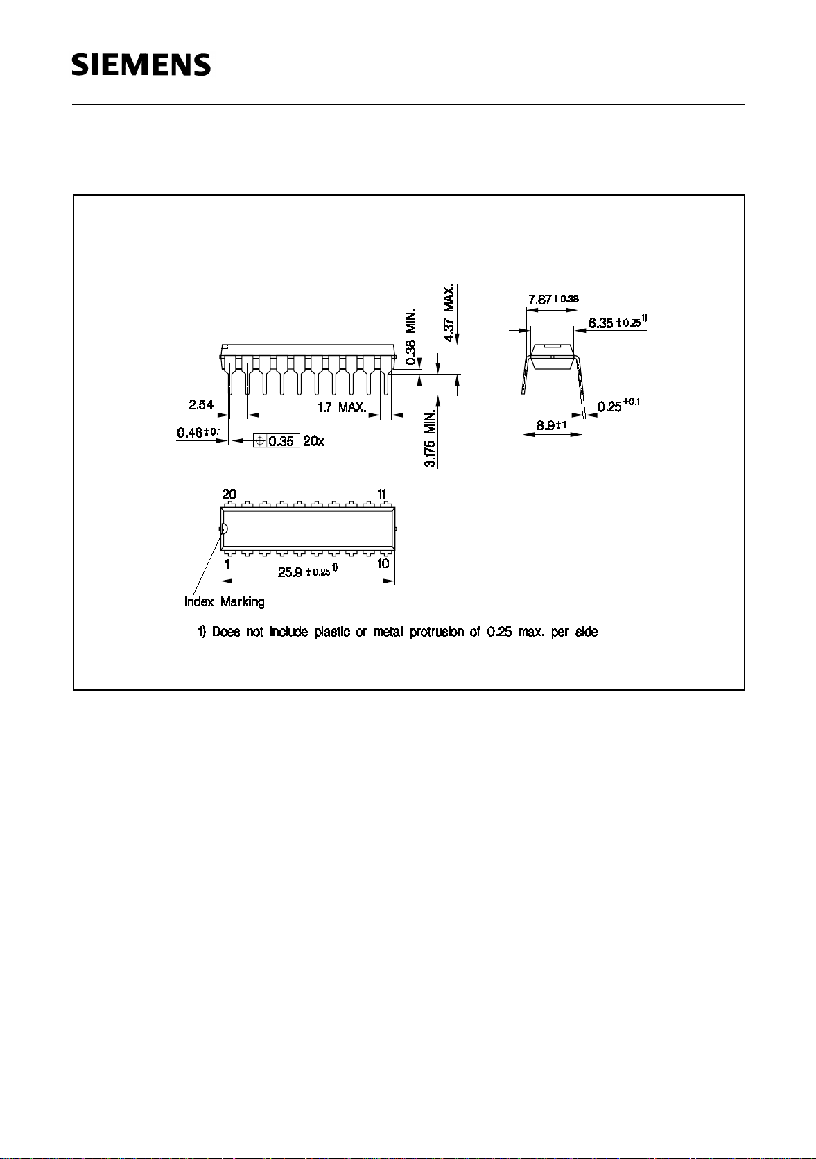
5 Package Outlines
P-DIP-20-5
(Plastic Dual In-line Package)
TDA 16888
Sorts of Packing
Package outlines for tubes, trays etc. are contained in our
Data Book “Package Information”.
GPD05587
Dimensions in mm
Semiconductor Group 38 Data Sheet 1998-05-06
Page 39
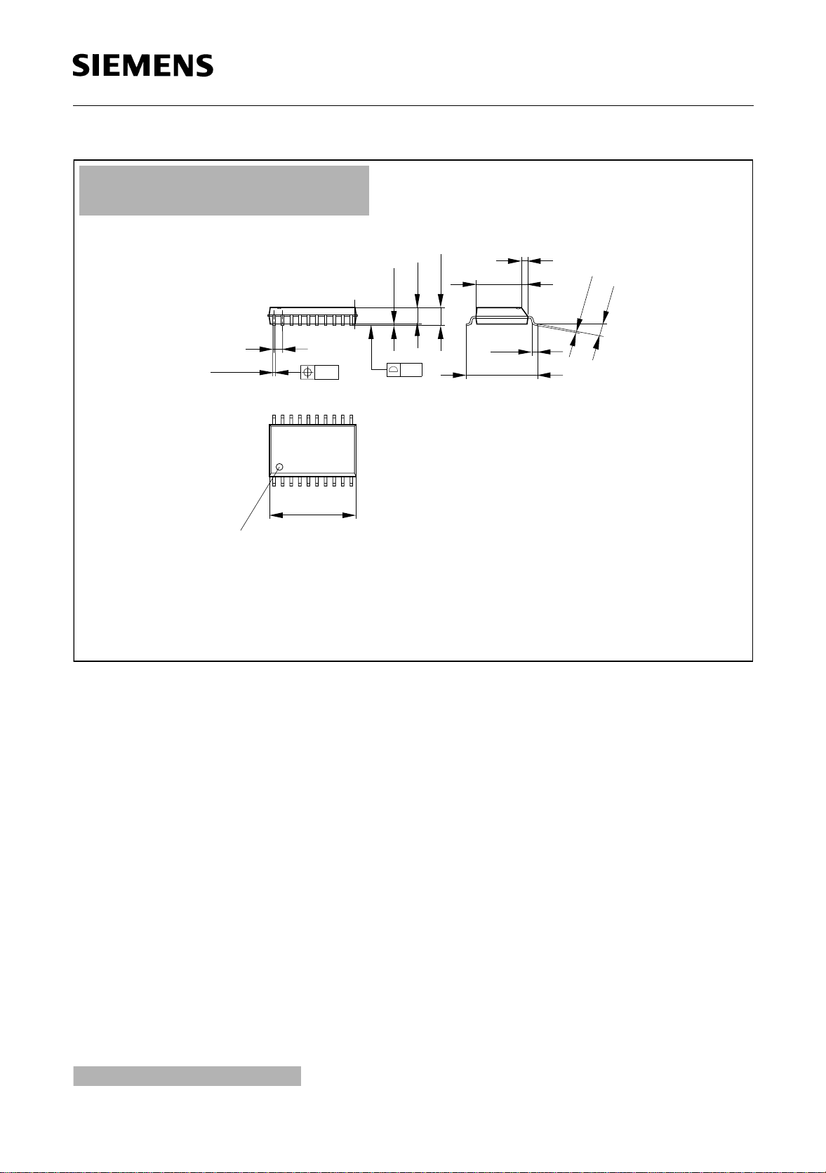
P-DSO-20-1
(Plastic Dual Small Outline)
1.27
+0.15
0.35
2)
0.2 24x
1120
-0.1
0.2
-0.2
2.45
0.1
7.6
2.65 max
10.3
0.35 x 45˚
1)
-0.2
+0.8
0.4
±0.3
GPS05094
+0.09
0.23
TDA 16888
8˚ max
110
12.8
-0.2
1)
Index Marking
1) Does not include plastic or metal protrusions of 0.15 max per side
2) Does not include dambar protrusion of 0.05 max per side
GPS 05094
Sorts of Packing
Package outlines for tubes, trays etc. are contained in our
Data Book “Package Information”.
SMD = Surface Mounted Device
Dimensions in mm
Semiconductor Group 39 Data Sheet 1998-05-06
 Loading...