

Page 1
.
I2C BUS CONTROL
.
STANDBY MODE
VIDEO SECTION
.
4 CVBS INPUTS, 3 CVBS OUTPUTS (ONE WITH
SELECT ABLE CHROMA TRAP FILTER)
.
4 Y/C INPUTS, 2 Y/C OUTPUTS
.
6dB GAIN ON ALL CVBS/Y AND C OUTPUTS
.
1 Y/C ADDER
.
2 RGB/FB INPUTS, 1 RGB/FB OUTPUT WITH
6dB AD JUST AB L E G AIN
.
VIDEO MUTING ON ALL THE OUTPUTS
.
2 SLOW BLANKING INPUTS/OUTPUTS
.
SYNC BOTTOM CLAMP ON ALL CVBS/Y
AND RGB INPUTS, AVERAGE ON C INPUTS
.
BANDWIDTH : 15MHz
.
CROSSTALK : 60dB Typ.
STV6411A
AUDIO/VIDEO SWITCH MATRIX
AUDIO SECTION
.
4 STEREO INPUTS, 3 STEREO OUTPUTS
(TWO WITH LEVEL ADJUS TM E N T )
.
MONO SOUND OUTPUT
.
STEREO TO MONO CAPABILITY ON BOTH
SCARTS
.
AUDIO MUTING ON ALL THE OUTPUTS
DESCRIPTION
The STV6411A is a highly integrated I2C bus-controlled aud io and vid eo sw it c h ma trix , opt im iz ed for
use in dig ital set-top bo x app licatio ns. I t prov ides all
the audio and video routings required in a full two
scart set- top box des ign. It is also fully pin compa tible with S TV 6410A, the three sc ar t ver sion.
TQFP64 (10 x 10 x 1.4mm)
(Full Plastic Quad Flat Pack)
ORDER CODE : STV6411AD
December 1998
1/20
Page 2
STV6411A
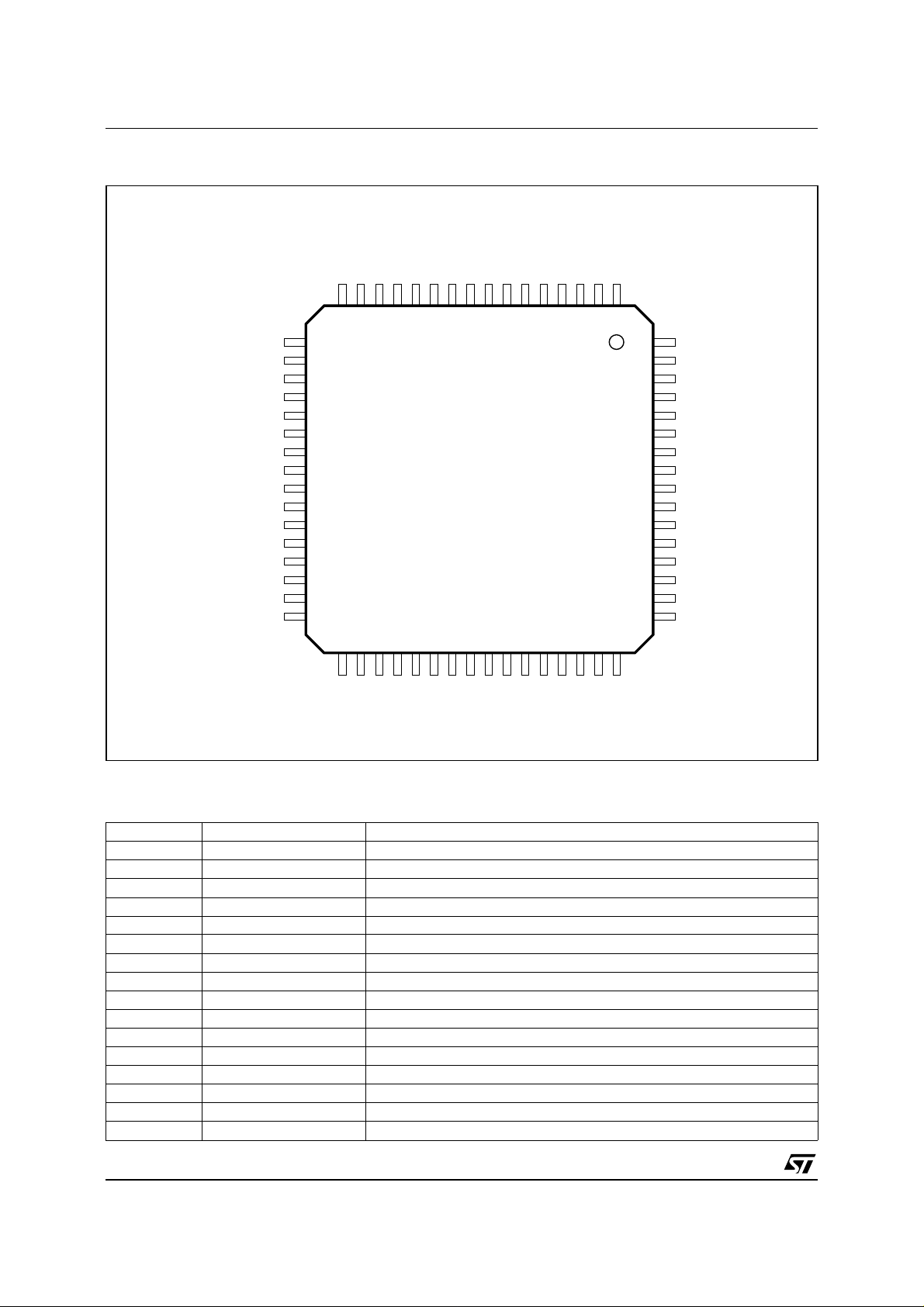
PIN CONNECTIONS
FBOUT_TV
FBIN_VCR (see Note 1)
FBIN_ENC
ADD
SCL
SDA
V
CC12
NC
SLB_TV
NC
SLB_VCR
RIN_VCR (see Note 1)
GNDV1
GIN_VCR (see Note 1)
NC
BIN_VCR (see Note 1)
Note 1 :
Pins (xx_VCR) identified as xx_AUX in STV6410 A.
CC2
V
NC
16151413121110
17
18
19
20
21
22
23
24
25
26
27
28
29
30
31
32
333435363738394041424344454647
CC1
V
CVBSIN_STB
CC3
NC
GNDV2
V
NC
NC
YCVBSIN_ENC
NC
YCVBSOUT_VCR
AOUT_RF
VOUT_RF
GNDV3
FILTER
987654321
LIN_STB
RIN_STB
YIN_ENC
CIN_ENC
RCIN_ENC
RIN_ENC
YCVBSOUT_TV
NC
COUT_VCR
LIN_ENC
BIN_ENC
GIN_ENC
RCOUT_TV
LOUT_TV
64
63
62
61
60
59
58
57
56
55
54
53
52
51
50
49
48
RIN_VCR
CIN_VCR
ROUT_TV
GOUT_TV
LOUT_VCR
BOUT_TV
ROUT_VCR
LOUT_CINCH
ROUT_CINCH
GNDA
RIN_TV
V
CCA
CIN_TV
LIN_TV
YCVBSIN_TV
V
REF
YCVBSIN_VCR
LIN_VCR
6411A-01.EPS
PIN LIST
Pin Number Symbol Description
1 RCOUT_TV Red/chroma Output, to TV Scart
2 LOUT_TV Audio Left Output, to TV Scart
3 YCVBSOUT_TV Y/CVBS Output, to TV scart
4 NC Not Connected
5 COUT_VCR Chroma Output, to VCR Scart
6 NC Not Connected
7 YCVBSOUT_VCR Y/CVBS Output, to VCR Scart
8 AOUT_RF Audio (L+R) Output to RF Modulator
9 VOUT_RF Video (CVBS) Output to RF Modulator
10 GNDV3 Video Switches Ground 3
11 FILTER Chroma Trap Filter
12 V
CCV3
13 NC Not Connected
14 GNDV2 Video Switches Ground 2
15 NC Not Connected
16 V
CCV2
2/20
Video Switches Supply 3 (8V)
Video Switches Supply 2 (8V)
6411A-01.TBL
Page 3
STV6411A
PIN LIST
(continued)
Pin Number Symbol Description
17 FBOUT_TV Fast Blanking Output, to TV Scart
18 FBIN_VCR (see Note 1) Fast Blanking Input, from VCR Scart
19 FBIN_ENC Fast Blanking Input, from Encoder
2
20 ADD I
21 SCL I
22 SDA I
23 V
CC12
C Bus IC Address Programmation
2
C Bus Clock
2
C Bus Data
Slow Blanking Power Supply (12V)
24 NC Not Connected
25 SLB_TV Slow Blanking Input/Ouput from TV
26 NC Not Connected
27 SLB_VCR Slow Blanking Input/Ouput from VCR
28 RIN_VCR (see Note 1) Red Input, from VCR Scart
29 GNDV1 Video Switches Ground 1
30 GIN_VCR (see Note 1) Green Input, from VCR Scart
31 NC Not Connected
32 BIN_VCR (see Note 1) Blue Input, from VCR Scart
33 V
CCV1
Video Switches Supply 1 (8V)
34 CVBSIN_STB CVBS Input from STB
35 NC Not Connected
36 YCVBSIN_ENC Y/CVBS Input from Encoder
37 NC Not Connected
38 YIN_ENC Y Input, from Encoder
39 RIN_STB Audio Right Input, from STB
40 CIN_ENC Chroma Input, from Encoder
41 LIN_STB Audio Left Input, from STB
42 RCIN_ENC Red/Chroma Input, from Encoder
43 RIN_ENC Audio Right Input, from Encoder
44 GIN_ENC Green Input, from Encoder
45 LIN_ENC Audio Left Input, from Encoder
46 BIN_ENC Blue Input, from Encoder
47 RIN_VCR Audio Right Input, from VCR Scart
48 CIN_VCR Chroma Input, from VCR Scart
49 LIN_VCR Audio Left Input, from VCR
50 YCVBSIN_VCR Y/CVBS Input from VCR Scart
51 V
REF
Voltage Reference Decoupling
52 YCVBSIN_TV Y/CVBS Input, from TV Scart
53 LIN_TV Audio Left Input, from TV Scart
54 CIN_TV Chroma Input, from TV Scart
55 V
CCA
Audio Switches Supply (8V)
56 RIN_TV Audio right input, from TV Scart
57 GNDA Audio Switches Ground
58 ROUT_CINCH Audio Right Output, to CINCH
59 LOUT_CINCH Audio Left Output, to CINCH
60 ROUT_VCR Audio Right Output, to VCR sCart
61 BOUT_TV Blue Output, to TV Scart
62 LOUT_VCR Audio Left Output, to VCR Scart
63 GOUT_TV Green Output, to TV Scart
64 ROUT_TV Audio Right Output, to TV Scart
Notes :
1. Pins (xx_VCR) identified as xx_AUX in STV6410A.
2. In application, all unused pins should be left open or high frequency bypass ed to ground.
6411A-01.TBL
3/20
Page 4
STV6411A
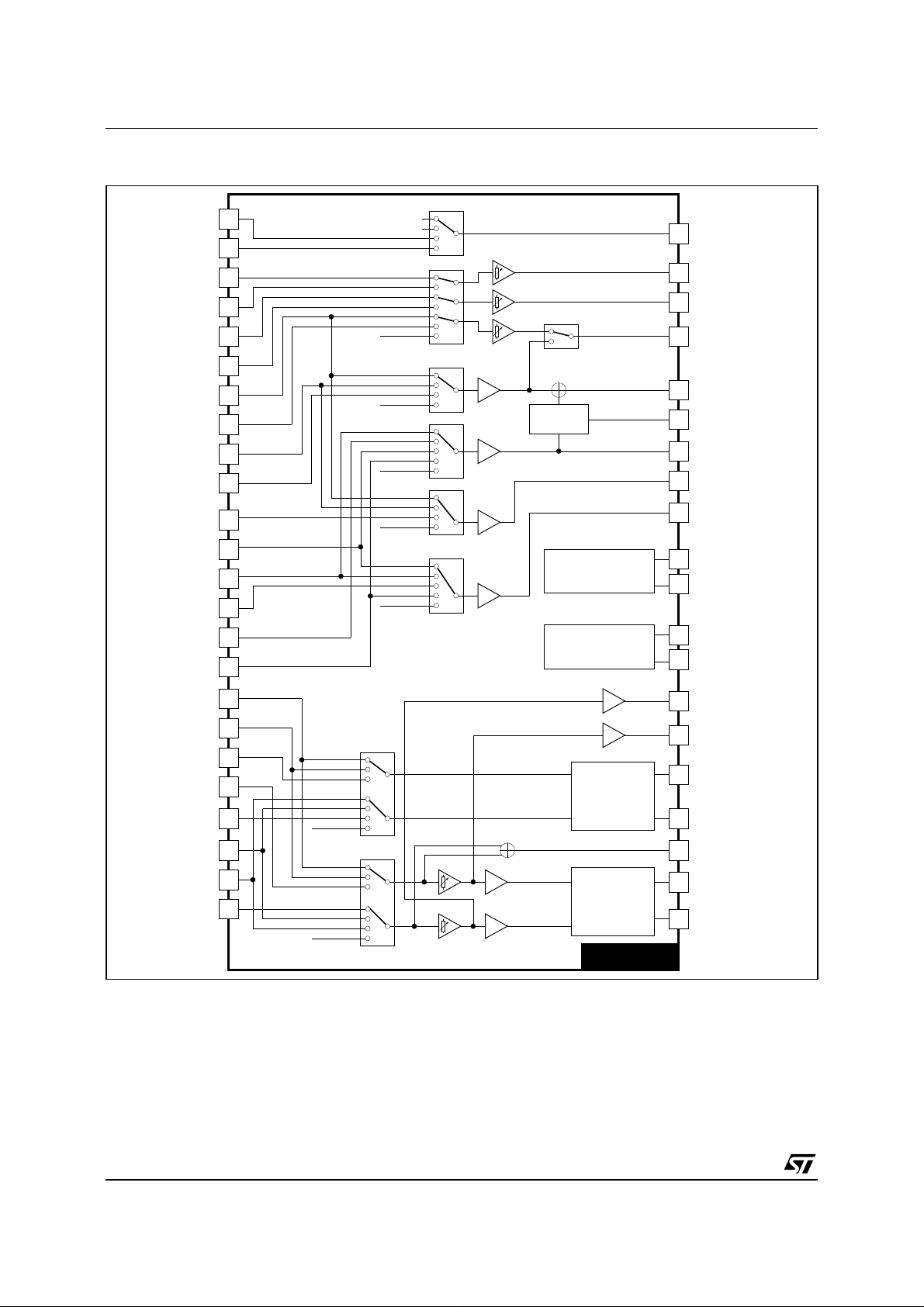
BLOCK DIAGRAM
FBIN_ENC
FBIN_VCR
(see Note 1)
BIN_ENC
BIN_VCR
(see Note 1)
GIN_ENC
GIN_VCR
(see Note 1)
RCIN_ENC
RIN_VCR
(see Note 1)
CIN_ENC
CIN_VCR
CIN_TV
19
18
46
32
44
30
42
28
40
48
54
4V
0V
B_ENC
B_ENC
B_VCR
G_ENC
G_VCR
R/C_ENC
R_VCR
MUTE
R/C_ENC
C_ENC
C_VCR
MUTE
CVBS/Y_ENC
CVBS/Y_VCR
CVBS_STB
Y_ENC
MUTE
R/C_ENC
C_ENC
C_TV
MUTE
FB SWITCH
RGB SWITCH
C SWITCH
Y/CVBS SWITCH
C SWITCH
17
FBOUT_TV
6dB
6dB
6dB
6dB
TRAP
6dB
6dB
61
BOUT_TV
63
GOUT_TV
1
RCOUT_TV
9
VOUT_RF
11
FILTER
3
YCVBS/OUT_TV
5
COUT_VCR
7
YCVBSOUT_VCR
CVBSIN_STB
YCVBSIN_ENC
YCVBSIN_TV
YCVBSIN_VCR
YIN_ENC
LIN_ENC
LIN_STB
LIN_TV
LIN_VCR
RIN_TV
RIN_STB
RIN_ENC
RIN_VCR
Note 1 :
Pins (xx_VCR) identified as xx_AUX in STV6410 A.
34
36
52
50
38
45
41
53
49
56
39
43
47
L_ENC
L_STB
L_TV
R_ENC
R_STB
R_TV
MUTE
L_ENC
L_STB
L_VCR
R_VCR
R_STB
R_ENC
MUTE
CVBS_STB
CVBS/Y_ENC
CVBS/Y_TV
Y_ENC
MUTE
VCR SWITCH
TV SWITCH
Y/CVBS SWITCH
-14dB
-14dB
25
SLOW BLANK,
I/O MONITOR
6dB
I2C BUS
DECODER
0/6dB
0/6dB
SLB_TV
27
SLB_VCR
21
SCL
22
SDA
59
LOUT_CINCH
58
ROUT_CINCH
62
LOUT_VCR
STEREO/
MONO
60
ROUT_VCR
8
AOUT_RF
0/6dB
STEREO/
MONO
0/6dB
2
64
LOUT_TV
ROUT_TV
STV6411A
6411A-02.EPS
4/20
Page 5
STV6411A
ABSOLUTE MAXIMUM RATINGS
Symbol Parameter Value Unit
AV
,VVCCSupply Voltage for Audio and Video Sections 10 V
CC
V
V
CC12
V
SLBK
VESD Maximum ESD Voltage allowed (100pF capacitor discharged
T
oper
T
stg
THERMAL DATA
Symbol Parameter Value Unit
R
th (j-a)
ELECTRICAL CHARACTERI STICS
= 25° C, AVCC = VVCC = 8V, V
T
amb
unless otherwise specified.
Symbol Parameter Test Conditions Min. Typ. Max. Unit
AV
CC
VV
CC
V
CC12
ACTIVE (all channels ON)
I
CCA
I
CCV
I
CC12
STANDBY (all channels OFF)
I
CCAstd
I
CCVstd
Voltage at Pin i to GND. Except SDA, SCL at 5.5V Max. 0, V
I
CC
Supply Voltage for Slow Blanking Sections 13.2 V
Voltage at slow blanking pins to GND 0, V
CC12
± 4kV
through 1.5kΩ serial resistor - Human Body Model)
Operating Ambient Temperature 0, +70
Storage Temperature -20, +150
Junction-ambient Thermal Resistance Max. 68
CC12
= 12V, R
= 10kΩ, RGA = 600Ω, RGV = 50Ω, R
LOUTA
LOUTV
Audio Operating Supply Voltage 7.5 8 8.5 V
Video Operating Supply Voltage 7.5 8 8.5 V
Slow Blanking Control Supply Voltage 11.2 12 12.8 V
Audio Supply Current AVCC = 8V, no input signal 10 15 mA
Video Supply Curr ent (I
12V Supply Current V
CCV1
+ I
CCV2
+ I
)VVCC = 8V, no input signal 65 80 mA
CCV3
= 12V
CC12
SlBlk input mode
SlBlk output mode, no load
2.023µAmA
0
Audio Supply Current in stand by mode AVCC = 8V 1.2 mA
Video Supply Current in stand by mode
(I
+ I
+ I
CCV1
CCV2
CCV3
)
VV
= 8V 9 mA
CC
o
= 4.7kΩ,
V
V
o
C
o
C
C/W
6411A-02.TBL
6411A-03.TBL
6411A-04.TBL
5/20
Page 6
STV6411A
ELECTRICAL CHARACTERI STICS
= 25°C, A VCC = VVCC = 8V, V
T
amb
(continued)
= 12V , R
CC12
= 10kΩ, RGA = 600Ω, RGV = 50Ω, R
LOUTA
LOUTV
= 4.7kΩ,
unless otherwise specified.
Symbol Parameter Test Conditions Min. Typ. Max. Unit
AUDIO SECTION
SVR100 Supply Voltage Rejection V
SVR1K Supply Voltage Rejection V
V
V
R
INmatch
F
INDC
INAC
R
range
Input DC Level AVCC = 8V VCC/2 V
Input signal amplitude 2V
Input Resistance 45 55 kΩ
IN
Input resistance matching ±1 ±10 %
Bandwith -3dB , 0.5V
Flatness Spread of gain in audio band 0.5V
Cs Channel Separation (from audio inputs)
= 500mV
RIPPLE
Gain = 0dB,
filter cap = 47µF
V
REF
V
filter cap = 220µF
REF
= 500mV
RIPPLE
Gain = 0dB
RMS
, 20Hz to 20kHz, Gain = 0dB 0.5 dB
RMS
= 0.5V
V
IN
RL =10kΩ, Gain = 0dB
RMS
Between L &R of TV outputs
Ci Channel Isolation from video inputs V
V
V
R
Output DC Level AVCC = 8V VCC/2 V
OUT
DC Offset change Switching between inputs 1 ±15 mV
OFF
Output Resistance 60 Ω
OUT
= 1 VPP, f = 15kHz, on one input,
IN
RL = 10kΩ, Gain = 0dB
eNI Equivalent Input Voltage Noise BW = 20Hz, 20kHz, Gain = 0dB 5 µV
G0 0dB Gain 0.5V
G
G
MATCH1
G
MATCH2
STEP
Step of Gain -14dB to +6dB 1.75 2 2.25 dB
Gain matching be tween different inputs
on one output
Gain matching between Left/Right
outputs of one input channel
VIN = 0.5V
VIN = 0.5V
, RL = 10kΩ, Gain = 0dB -0.5 +0.5 dB
RMS
RMS
RMS
THD Total Harmonic Distorsion 1kHz, LPF @ 80kHz
= V
= 0.5V
OUT
= 2V
OUT
, THD = 0.3%, Gain = 0dB 2 2.25 kΩ
RMS
RMS
V
R
Output clipping Level THD = 0.2%, 1kHz 2.1 2.25 V
CL
Output Load Resistance VIN = 1V
L
Mute Mute Suppression V
V
IN
VIN = V
= 0.5V
IN
at f = 100Hz,
RMS
60 72
82
at f = 1kHz,
RMS
70 80 dB
, RL = 10kΩ, Gain = 0dB 50 kHz
, f = 1kHz, on on e input,
807090
74
70 85 dB
, 1kHz, Gain = 0dB -0.5 0.5 dB
, 1kHz, Gain = 0dB -0.5 0.5 dB
RMS
RMS
0.002
0.003
0.05 %
, on one input 90 dB
dB
dB
RMS
dB
dB
%
RMS
6411A-05.TBL
6/20
Page 7

STV6411A
ELECTRICAL CHARACTERI STICS
= 25°C, A VCC = VVCC = 8V, V
T
amb
(continued)
= 12V , R
CC12
= 10kΩ, RGA = 600Ω, RGV = 50Ω, R
LOUTA
LOUTV
= 4.7kΩ,
unless otherwise specified.
Symbol Parameter Test Conditions Min. Typ. Max. Unit
VIDEO SECTION
V
DCIN
I
CLAMP
I
LEAK
C
IN
V
IN
DYN Dynamic Output Signal VVCC = 8V 3 4 V
BW Bandwidth at -3dB Y/CVBS
CT Crosstalk Isolation between Channels V
R
OUT
R
LOAD
G
RGB
G
RGBM
G
RGBSTEP
G
YCVBS
G
YCVBSM
DC
OUT
DC
OUT RF
DPHI Differential Phase V
DG Differential Gain V
Mute Mute Suppression V
I
VOUT
CHROMA SECTION
V
DCIN
R
IN
C
IN
V
IN
Dyn Dynamic Output Signal 3 3.8 V
DC
OUT
CBW Chroma Bandwidth C
CT Crosstalk Isolation between channel V
R
OUT
G
OUTC
G
CM
Mute Mute Suppression V
CtoYdel Chroma to luma delay, source Y/C Pin other than RF_OUT 1,
CtoYdel Chroma to luma delay, source Y/C Pin RF_OUT ±4 ±20 ns
DC Input Level Bottom Synch Pulse 2 V
Clamping current at V
Input Leakage Current VIN = V
- 400mV 1 2 mA
DCIN
+ 1V 1 10 µA
DCIN
Input Capacitance 2 pF
Max Input Signal VVCC = 8V 1.5 2 V
15
RGB
Y/C mixer (on RF out)
VIN = 1V
VIN = 1VP
V
on one input
PP
P
= 1VPP, V
INY
= 1VPP at f = 5MHz,
IN
INC
= muted
18
15
18
10
15
50 60 dB
Output Resistance 50 Ω
Load Impedance 1 4.7 ∞ kΩ
Gain at RGB outputs VIN = 1VPP, gain set to 6dB 5.5 6 6.5 dB
Gain matching between R, G, B VIN = 1VPP, gain set to 6dB -0.3 0 0.3 dB
Step of Gain 3dB to 6dB 0.75 1 1.25 dB
Gain on Y/CVBS channels VIN = 1V
Gain matching between Y, CVBS inputs VIN = 1V
PP
PP
5.5 6 6.5 dB
-0.5 0 0.5 dB
DC Output Voltage Bottom sync pulse 1.1 1.3 V
RF Output Voltage Bottom sync pulse 1.5 1.8 V
= 1VPP, 4.43MHz 0.7 °
IN
= 1VPP, 4.43MHz 0.4 %
IN
Output Current V
= 1VPP at f = 5MHz,
IN
on one input
@ +1V 1.5 2.5 mA
OUT DC
-55 dB
DC Input Level 3 V
Input Resistance 45 55 kΩ
Input Capacitance 2 pF
Max Input Signal 1.5 2 V
DC Output Voltage 1.9 2.3 V
= 1VPP at - 3dB 10 19 MHz
IN
= 1VPP at f = 5MHz,
IN
on one input
52 dB
Output Resistance 50 Ω
Gain at OUTC VIN = 1V
Gain matching between C inputs VIN = 1V
= 1VPP at f = 5MHz,
IN
on one input
PP
PP
5.5 6 6.5 dB
-0.5 0 0.5 dB
55 dB
±4 ±20 ns
V
@ 5MHz
PP
PP
PP
MHz
MHz
MHz
PP
6411A-06.TBL
7/20
Page 8

STV6411A
ELECTRICAL CHARACTERI STICS
= 25°C, A VCC = VVCC = 8V, V
T
amb
(continued)
= 12V , R
CC12
= 10kΩ, RGA = 600Ω, RGV = 50Ω, R
LOUTA
LOUTV
= 4.7kΩ,
unless otherwise specified.
Symbol Parameter Test Conditions Min. Typ. Max. Unit
SLOW BLANKING SECTION
INPUT (Input mode V
SLBlow Input Low Level Threshold 2.5 3.25 4 V
SLBhigh Input High Level Threshold 7.5 8.25 9 V
I
IN
Input current 50 100 µA
OUTPUT (Output mode V
SLBLOW Output Low Level (int. TV) 0 0.02 1.5 V
SLBMED Output Med Level (ext. 16/9) 5 5.75 6.5 V
SLBHIGH Output High Level (ext. 4/3) 10 11 12 V
FAST BLANKING SECTION
INPUT (Input mode V
FBlow/high Input Low/High Level Threshold 0.4 0.7 0.9 V
I
IN
Input current 210µA
OUTPUT (Output mode V
Output Low Level IIN = 1.0mA
Output High Level I
Fast blanking to RGB delay At 50% on digital RGB transients,
DEL
Fast Blanking transitions at FB output
Rise Time
FB
FB
FB
FB
LOW
HIGH
TRANS
Fall Time
ADDRESS SELECTION INPUT
ADDsel_L Address selection low level 0 0.2 V
ADDsel_H Address selection high level 4 V
I
LEAK
Leakage Current 10 µA
= 8V ±5%)
CC8
CC12
= 8V ±5%)
CCV
CCV
= 12V ±5%, V
= 8V ±5%, R
= 8V ±5%, R
CC8
> 1kΩ)
LOAD
> 10kΩ)
LOAD
00.7
IIN = 0.2mA
= 1.0mA 3.6 4 4.4 V
OUT
30 ns
at 2.7V
on FB fall C
C
FB rise transient, at 1.5V
ON
= 10pF max
LOAD
between 10% and 90%
= 10pF max
LOAD
between 90% and 10%
30
30
0.3VV
CC
(8V)
ns
ns
V
6411A-07.TBL
8/20
Page 9

STV6411A
ELECTRICAL CHARACTERI STICS
= 25°C, A VCC = VVCC = 8V, V
T
amb
(continued)
= 12V , R
CC12
= 10kΩ, RGA = 600Ω, RGV = 50Ω, R
LOUTA
LOUTV
= 4.7kΩ,
unless otherwise specified.
Symbol Parameter Test Conditions Min. Typ. Max. Unit
2
C BUS CHARACTERISTICS
I
SCL
V
V
f
SCL
SDA
V
V
V
C
TIMING
t
LOW
t
HIGH
t
SU,DAT
t
HD,DAT
t
SU,STO
t
BUF
t
HD,STA
t
SU,STA
Low Level Input Voltage -0.3 1.5 V
IL
High Level Input Voltage 3 5.5 V
IH
Input Leakage Current VIN = 0 to 5.5V -10 0 10 µA
I
LI
Clock Frequency 0 100 kHz
Input Rise Time 1.5V to 3V 1 µs
t
R
Input Fall Time 1.5V to 3V 300 ns
t
F
Input Capacitance 10 pF
C
l
Low Level Input Voltage -0.3 1.5 V
IL
High Level Input Voltage 3 5.5 V
IH
Input Leakage Current VIN = 0 to 5.5V -10 0 10 µA
I
LI
Input Capacitance 10 pF
C
l
Input Rise Time 1.5V to 3V 1 µs
t
R
Input Fall Time 1.5V to 3V 300 ns
t
F
Low level Output Voltage IOL = 3mA 0.4 V
OL
Output Fall Time 3V to 1.5V 250 ns
t
F
Load Capacitance 400 pF
L
Clock Low Period 4.7 µs
Clock High Period 4 µs
Data Set-up Time 250 ns
Data Hold Time 0 340 ns
Set-up Time from Clock High to Stop 4 µs
Start Set-up Time following a Stop 4.7 µs
Start Hold Time 4 µs
Start Set-up Time following Clock Low to High Transition 4.7 µs
6411A-08.TBL
9/20
Page 10

STV6411A
I2C BUS SELECTION
Data transfers follow the usual I2C format: after the start condition (S), a 7-bit slave address is sent, followed
by an eighth bit which is a data direction bit (W). A 8-bit subadress is sent to select a register, followed by
a 8-bit data word to put in it.
The IC’s I2C bus decoder permits the automatic incrementation mode in write mode.
String Format
Write only mode (S : start condition, P : stop condition, A : acknowledge)
S SLAVE ADDRESS 0 A SUBADDRESS A DATA A P
Read only mode
S SLAVE ADDRESS 1 A DATA A P
Slave Address
Address A6 A5 A4 A3 A2 A1 A0
Value 100101X
Auto Increment Mode
S SLAVE ADDRESS 0 A SUBADDRESS A DATA0 A DATA1 A ........ DATAN A P
I2C Bus Address
Write Address : 1001 01X0
Read Address : 1001 01X1
Address Selection Pin Grounded : X = 0, write address = 94HEX, read address = 95HEX
Address Selection Pin to Supply : X = 1, write address = 96HEX, read address = 97HEX
Input Signals Summary
Reg.
Addr.
(HEX)
DATA D7 DATA D6 DATA D5 DATA D4 DATA D3 DATA D2 DATA D1 DATA D0
00
01
02
03 Not used
04 TV RGB Output Control TV FB Output Control RGB Gain
05
06 Not used Not used
07
08 Not used Not used Not used Not used Not used Not used
TV/Cinch Audio Level Adjustment
Identical values should be written
STV6410A
only
VCR
Output
OFF
(Write Mode)
to both registers
VCR Mono
TV Chroma
Mute
STV6410A
only
STV6410A
only
Set to 1
0/6dB
TV Gain
0/6dB
Cinch Gain
STV6410A
only
Y/CVBS & Chroma TV Outputs Control TV RF Ouput Control
STV6410A
only
TV
Output
OFF
ENCOD
Clamp
disable
TV Mono TV Audio Outputs Control
Not used Cinch Audio Outputs Control
VCR Audio Outputs Control
STV6410A
only
VCR
Chroma
Mute
Slow Blanking
VCR SCART
TV
Clamp
disable
ASTB
Clamp
disable
VCR Y/CVBS &
Chroma Outputs Control
Slow Blanking
TV SCART
VCR
Clamp
disable
RF Mod
Output OFF
Not used data must be put to "0"
TV R/C
Ouput
Control
R/Csub
Encoder
Clamp
RGB
Clamp
disable
CINCH
Output OFF
10/20
Page 11

STV6411A
I2C BUS SELECTION
Input Signals
(Write Mode)
(continued)
Data Byte
TV Audio Output
Reg.
Addr.
(HEX)
00 Audio Output selection 3 X X X X X 0 0 0 Muted
Description Bits
Stereo or Mono Mode 1 X X X X 0 X X X 0 = Stereo
6dB Extra Gain 1 X X X 0 X X X X 0 = 0dB
Level Adjustment 3 0 0 0 X X X X X 0dB Adjustment
d7 d6 d5 d4 d3 d2 d1 d0
X X X X X 0 0 1 NOT ALLOWED
X X X X X 0 1 0 VCR inputs selected
X X X X X 0 1 1 ASTB inputs selected
X X X X X 1 0 0 NOT ALLOWED
X X X X X 1 0 1 Encoder inputs selected
X X X X X 1 1 0 NOT ALLOWED
X X X X X 1 1 1 NOT ALLOWED
X X X X 1 X X X 1 = Mono
X X X 1 X X X X 1 = +6dB
1 1 1 X X X X X -14dB Adjustment (-2dB/step)
Data
Audio Cinch Output
Reg.
Addr.
(HEX)
01 Audio Output Selection
Description Bits
Level Adjustment
6dB Extra Gain 1 X X X 0 X X X X 0 = 0dB
d7 d6 d5 d4 d3 d2 d1 d0
3 d7 d6 d5 X X d2 d1 d0 Used in STV6410A. In STV6411A
X X X 1 X X X X 1 = +6dB
Data
Comments
Comments
applic ations d7d6d5 d2d1d0 dat a should
be identical to register 00H.
VCR Audio Outputs Selection
Reg.
Addr.
(HEX)
02 VCR Audio Output
Description Bits
Selection
Used in STV6410A.
For STV6411A
applications, should be
set to mute value
(XX000XXX).
Data
d7 d6 d5 d4 d3 d2 d1 d0
3 XX000000Muted
X X 0 0 0 0 0 1 NOT ALLOWED
X X 0 0 0 0 1 0 NOT ALLOWED
X X 0 0 0 0 1 1 ASTB inputs selected
X X 0 0 0 1 0 0 TV inputs selected
X X 0 0 0 1 0 1 Encoder inputs selected
X X 0 0 0 1 1 0 NOT ALLOWED
X X 0 0 0 1 1 1 NOT ALLOWED
X 0 0 0 0 X X X 0 = Stereo
X 1 0 0 0 X X X 1 = Mono
3 X X 0 0 0 X X X Muted
X X 0 0 1 X X X NOT ALLOWED
X X 0 1 0 X X X NOT ALLOWED
X X 0 1 1 X X X NOT ALLOWED
X X 1 0 0 X X X NOT ALLOWED
X X 1 0 1 X X X NOT ALLOWED
X X 1 1 0 X X X NOT ALLOWED
X X 1 1 1 X X X NOT ALLOWED
Comments
11/20
Page 12

STV6411A
I2C BUS SELECTION
(continued)
TV Video Output
Reg.
Addr.
(HEX)
03 R/C TV Output Selection 1 X X X X X X X 0 Red signal selected
RF output : adder control and
chroma subcarrier filter selection
Y/CVBS output and chroma
signal selection
Chroma switch muting 1 X 0 X X X X X X Chroma Output controlled by
04 ENCODER R/Csub Clamp 1 X X X X X X X 0 Bottom Level Clamp
Used in STV6410A.
In STV6411A applications should
be set to zero (XXXXXX0X).
RGB output Gain 2 X X X X 0 0 X X +6dB gain
FB Output 2 X X 0 0 X X X X FB forced to low level
RGB ouputs selection 2 0 0 X X X X X X Muted
Description Bits
2 X X X X X X 0 X CVBS to RF output
3 X X 0 0 0 X X X Y/CVBS & chroma muted
1 X X X X X X 0 X Bottom Level Clamp
d7 d6 d5 d4 d3 d2 d1 d0
X X X X X X X 1 Chroma signal selected
X X X X X X 1 X Y+C to RF output
X X X X X 0 X X Filter not active
X X X X X 1 X X Filter active
X X 0 0 1 X X X NOT ALLOWED
X X 0 1 0 X X X NOT ALLOWED
X X 0 1 1 X X X Y/CVBS _VCR & C_VCR
X X 1 0 0 X X X CVBS_ASTB & Chroma muted
X X 1 0 1 X X X Y/CVBS_ENC & R/C_ENC
X X 1 1 0 X X X Y_ENC & C_ENC
X X 1 1 1 X X X NOT ALLOWED
X 1 X X X X X X Chroma Output forced to mute
X X X X X X X 1 Average Level Clamp
X X X X X X 1 X Average Level Clamp
X X X X 1 1 X X +3dB gain (1dB/Step)
X X 0 1 X X X X FB forced to high level
X X 1 0 X X X X FB from Encoder
X X 1 1 X X X X FB from AUX
0 1 X X X X X X RGB_Encoder selected
1 0 X X X X X X RGB_AUX selected
1 1 X X X X X X NOT ALLOWED
Data
Comments
d5d4d3 from register 03
12/20
Page 13

STV6411A
I2C BUS SELECTION
(continued)
VCR Video Outputs
Reg.
Addr.
(HEX)
05 VCR Y/CVBS & Chroma
Outputs Selection
VCR Chroma Output Muting 1 1 0 0 0 0 X X X Chroma Output controlled by
Used in STV6410A.
For STV6411A applications
should be set to mute value
(X000XXXX).
Description Bits
Data
d7 d6 d5 d4 d3 d2 d1 d0
3 1 0 0 0 X 0 0 0 Y/CVBS & chroma muted
1 0 0 0 X 0 0 1 NOT ALLOWED
1 0 0 0 X 0 1 0 NOT ALLOWED
1 0 0 0 X 0 1 1 NOT ALLOWED
1 0 0 0 X 1 0 0 CVBS_ASTB & chroma muted
1 0 0 0 X 1 0 1 Y/CVBS_ENC & R/C_ENC
1 0 0 0 X 1 1 0 Y_ENC & C_ENC
1 0 0 0 X 1 1 1 Y/CVBS_TV & C_TV
d2d1d0 from register 05
1 X X X 1 X X X Chroma Output forced to mute
3 X 0 0 0 X X X X Y/CVBS & chroma muted
X 0 0 1 X X X X NOT ALLOWED
X 0 1 0 X X X X NOT ALLOWED
X 0 1 1 X X X X NOT ALLOWED
X 1 0 0 X X X X NOT ALLOWED
X 1 0 1 X X X X NOT ALLOWED
X 1 1 0 X X X X NOT ALLOWED
X 1 1 1 X X X X NOT ALLOWED
Comments
Slow Blanking Switches
Reg.
Addr.
(HEX)
06 Slow Blanking TV SCART 2 X X 0 0 X X 0 0 Input mode
Slow Blanking VCR SCART 2 X X 0 0 0 0 X X Input mode
Used in STV6410A.
For STV6411A applications
should be set to input mode
(XX00XXXX).
Description Bits
2 X X 0 0 X X X X Input mode
d7 d6 d5 d4 d3 d2 d1 d0
X X 0 0 X X 0 1 Output < 2V
X X 0 0 X X 1 0 Output 16/9 format
X X 0 0 X X 1 1 Output 4/3 format
X X 0 0 0 1 X X Output < 2V
X X 0 0 1 0 X X Output 16/9 format
X X 0 0 1 1 X X Output 4/3 format
X X 0 1 X X X X NOT ALLOWED
X X 1 0 X X X X NOT ALLOWED
X X 1 1 X X X X NOT ALLOWED
Data
Comments
13/20
Page 14
STV6411A
2
I
C BUS SELECTION
(continued)
Standby Modes Sele c tion
Reg.
Addr.
(HEX)
07 VCR Clamps Disabling
(RGB inputs)
VCR Clamps Disabling 1 X 1 X X X X 0 X Clamp Active
ASTB Clamps Disabling 1 X 1 X X X 0 X X Clamp Active
TV Clamps Disabling 1 X 1 X X 0 X X X Clamp Active
Encoder Clamps Disabling 1 X 1 X 0 X X X X Clamp Active
TV/RGB Output Disabling 1 X 1 0 X X X X X Audio & Video Outputs ON
VCR Output Disabling 1 0 1 X X X X X X Audio & Video Outputs ON
08 CINCH Output Disabling 1 X 1 X X X X X 0 CINCH Output ON
RF MOD Output Disabling 1 X 1 X X X X 0 X RF MOD Output ON
Description Bits
1 X 1 X X X X X 0 Clamp Active
d7 d6 d5 d4 d3 d2 d1 d0
X1XXXXX1Clamp Disabled
X 1 X X X X 1 X Clamp Disabled
X 1 X X X 1 X X Clamp Disabled
X 1 X X 1 X X X Clamp Disabled
X1X1XXXXClamp Disabled
X 1 1 X X X X X Audio & Video Outputs OFF
1 1 X X X X X X Audio & Video Outputs OFF
X 1 X X X X X 1 CINCH Output OFF
X 1 X X X X 1 X RF MOD Output OFF
Data
Comments
Output Signals
(Read Mode)
Data Byte
Reg.
Addr.
(HEX)
Description Bits
Slow Blanking TV SCART 2 X X X X X X 0 1 Input < 2V
Slow Blanking VCR SCART 2 X X X X 0 1 X X Input < 2V
d7 d6 d5 d4 d3 d2 d1 d0
X X X X X X 1 0 Input 16/9 format
X X X X X X 1 1 Input 4/3 format
X X X X 1 0 X X Input 16/9 format
X X X X 1 1 X X Input 4/3 format
Data
Power-on Reset - Bus Register Initial Conditions
Power on reset is active when the power supply voltage is below (Tbf) volts.
Not significant bits (X) are preset to "0"
Register Address HEX
00 00000000
01 00000000
02 00000000
03 00000000
04 00000000
05 00000000
06 00000000
07 00000000
08 00000000
d7 d6 d5 d4 d3 d2 d1 d0
DATA
Comments
14/20
Page 15

INPUT/OUTPUT GROUPS
Figure 1 :
Bottom Cl amp e d Video Inputs
(Pins 30, 32 ,3 4, 36, 3 8, 44 , 4 6, 50 , 52 )
Figure 2 :
STV6411A
Average Clamped Video Inputs
(Pins 40, 48, 54)
Protected Pad
Figure 3 :
VCC 8V
VCC 8V VCC 8V
15k
W
tri
Audio Inputs (5 Stereo)
(Pins 39-41, 47-49, 53-56)
I
B
50k
W
2V + V
D
VCC/2
Protected Pad
6411A-03.EPS
Figure 4 :
VCC 8V
VCC 8V
I
B
Audio Outputs (4 Stereo +1)
(Pins 58, 59, 60-62, 8)
25k
60
W
tri
25k
W
3V
6411A-04.EPS
VCC 8V
W
Protected Pad
Figure 5 :
VCC 8V
Trap Filter (Pin 11)
1k
W
100
W
Protected Pad
VCC 8V
6411A-05.EPS
Figure 6 :
6411A-07.EPS
Video Outputs
(Pins 61, 63, 1, 3, 5, 7, 9)
VCC 8V
50
W
5k
W
5k
W
Protected Pad
Protected Pad
6411A-06.EPS
VCC 8V
6411A-08.EPS
15/20
Page 16

STV6411A
INPUT/OUTPUT GROUPS
External Capacitor (Pin 51)
Figure 7 :
Figure 9 :
V
REF
VCC 8V
I
B
I
B
Input Fast Blanking (Pins 18, 19)
VCC 8V
(continued)
VCC 8V
40k
W
40k
W
Protected Pad
Figure 8 :
6411A-09.EPS
Figure 10 :
Slow Blanking (Pins 25, 27)
VCC 12V
1k
W
25k
W
80k
W
80k
W
Protected Pad
Output Fast Blanking (Pin 17))
1k
W
VCC 8V
VCC 12V
6411A-10.EPS
Protected Pad
Figure 11 :
VCC 8V
Protected Pad
2
C Bus (ADD) (Pin 20)
I
10k
W
6411A-11.EPS
Figure 12 :
6411A-13.EPS
25k
W
2
C Bus (SCL) (Pin 21)
I
VCC 8V
Protected Pad
10k
50
W
Protected Pad
6411A-12.EPS
W
6411A-14.EPS
16/20
Page 17

STV6411A
INPUT/OUTPUT GROUPS
2
C Bus (SDA) (Pin 22)
Figure 13 :
I
APPLICATION DIAGRAM
SCART1
TV
RF MOD
(continued)
VCC 8V
Protected Pad
R/C
G
B
FAST BLANK
CVBS/Y
AUDIO L
AUDIO R
CVBS/Y
AUDIO L
AUDIO R
SLOW BLANK
CVBS
AUDIO L+R
Acknowledge
10k
W
6411A-15.EPS
AUDIO L
AUDIO R
R
C
STV6411A
R, G, B, FB
SWITCHES
CVBS/Y
SWITCHES
CHROMA
SWITCHES
AUDIO
SWITCHES
SLOW BLANK,
I/O CONTROL
R/C
G
B
FAST BLANK
CVBS/Y
C
AUDIO L
AUDIO R
Y
CVBS
AUDIO L
AUDIO R
R
G
B
FAST BLANK
CVBS/Y
AUDIO L
AUDIO R
C
CVBS/Y
C
AUDIO L
AUDIO R
SLOW BLANK
CINCH
OUTPUT
ENCODER
ANALOG
STB
SCART2
VCR
6411A-16.EPS
17/20
Page 18
STV6411A
APPLICATION NOTE
1 - Audio Part
1.a - Inputs
The audio inputs are designed to follow sources up
to (at least) 2V
expected DC level of V
the device is providing this DC polarization. That
means that in most of the cases the inputs are AC
coupled via chemical capacitors. The recommended values are 1µF, 2 .2µF or 4.7µF (internal
polar. is made via a 50kΩ resistor). I want to point
out that the internal polarization is filtered by an
external capacitor (on Pin called ‘V
pacitor contribute to good performance of the device. Its value should be 47µF or more (coupled
with an 47nF HF cap. for internal video referenc es).
Figure 14 :
L/R Audio
Audio Inputs
12k
(that is around 6VPP) with an
RMS
/2 (4V typ.). That’s why
CC
220
W
4.7mF
W
’). This ca-
REF
Audio In
2 - Video Part
2.a - Inputs
Video inputs need to be AC coupled. But only some
small capacitor values are requested thanks to the
internal clamps provided by these devices. Usually
some 100nF HF capacitors (47nF to 220nF) are
enough to provide good performances on Y,
CVBS,RGB and C inputs.
Chrominan ce in puts : - a verage clam p - that mean s
that the DC is meas ured as the avera ge value of the
input signal and set to an internal reference (close
to 3V). The dy na mi c allowed is more than 1.5V .
RGB, Y, CVBS inputs : - bottom sync top clam p that means that the DC level is measured at the
lowest value of the input signal and set to an
internal reference (close to 2V). The dynamic allowed is more than 1.5V.
Figure 16 :
Y/C/CVBS/RGB
Video Inputs
220
100nF
W
Video In
STV6411A
NB: In some particular cases (loopback from outputs to inputs) the AC coupling capacitor can be
removed... but some small offsets in the audio
chain can cause some noise while switching from
one input to another.
1.b - Outputs
Audio output buffers are able to provide more than
2.1V
(around 6VPP) on a typical load of 10k
RMS
(in fact a 2kΩ load is acceptable). The DC level is
once more V
/2 for best dynamic performance.
CC
Usually some AC coupling capacitors are used at
the outputs. To drive some typical 10kΩ loads, it is
normal to use capacitors with value 5 t o 10 times
the value of the input capacitors. That gives a value
between 4.7µF and 47µF. Moreover it can be a
good idea to insert resistors ( 220Ω or 470Ω) in the
audio outputs. That will provide a protection for
output stages. No external drivers or buffers are
needed in typical use of the device.
Figure 15 :
Audio Out
Audio Outputs
4.7mF
470
W
L/R Audio
STV6411A
75
W
6411A-17.EPS
2.b - Outputs
On thes e devices the v ideo outputs are NOT AB LE
to drive 150Ω. That means that external buffers (one
simple NPN-Transistor per output) are needed. To
reduce the external components, the output DC
level have been chose n to allow a di rect driv e of the
Ω
base of the output follower (NPN). The emitters of
the NPN s wil l be polarized t o gr ound via 1kΩ resistors (more or le ss) and will driv e the outputs throug h
some 75Ω resistors. Do not f or get t o bufferize your
favourite UHF modulator video input...
Chrominance outputs have a DC of 2.3V (it is an
average value) and Luminance type output have a
DC of 1.3V (it is a bottom value).
Figure 17 :
Video Out
Video (and Fast Blanking) Outputs
75
W
(4.7kW)1k
W
STV6411A
6411A-18.EPS
STV6411A
6411A-19.EPS
Video
6411A-20.EPS
18/20
Page 19

STV6411A
APPLICATION NOTE
(continued)
2.c - Fast Blanking
Fast Blanking signal is used to make an equipment
consider its RGB inputs for full-screen display or
fast insertion (OSD, etc.). The output of such s ignal
is exactly managed in the same way as RGB (that
is important for levels and delays).
The input is DC coupled (insert a few hundreds
ohms resistors for external input).
2.d - Slow Blanking
Slow Blanking signal is used to make an equipment
consider an external input (e.g. CVBS and
SOUND). The input/output of such signal is very
simple, DC coupled (insert a few hundreds ohms
resistors for external I/O). Notice that this function
is requesting a 12V power supply (on Pin V
CC12
This pin can be left open (not pulled down) if this
function is not used.
2
3 - I
C Bus
3.a - Address
You can choose the address of the device by
setting the Pin ADD to ground or to V
DD
selects 94h and the latter selects 96h. These values correspond to the writeable (or control) registers. Change the lowest bits to ‘1’ (that gives 95h
and 97h) to read the readable register of the device.
One device will answer (acknowledge) to its both
addresses 94h and 95h or 96h and 97h.
3.b - Write Mode
This mode is used to c ontrol the devic e, to select
switches positions, gains, etc.
Send a start condition, the addr ess of the dev ice,
the address of the register (its number), and the
data to put in it. At t his point you can send a stop
or send the data of the following registers (that is
what we call auto-increment).
).
3.c - Read Mode
This mode is used to read some data such as
slow-blanking input signals.
Send a start condition, the address of the device
(+1) and then send one byte clock to read the
unique data register.
. The former
N.B.: Do not forget your favourite ESD protections for I/O signals of plugs.
19/20
Page 20

STV6411A
PACKAGE MECHANICAL DA TA
64 PINS - FULL PLASTIC QUAD FLAT PACK (TQFP )
64 49
1
e
A
A2
A1
0,10 mm
.004 inch
E3
E1
SEATING PLANE
B
E
48
33
c
L1
L
0,25 mm
.010 inch
K
GAGE PLANE
Dimensions
16
17 32
D3
D1
D
Millimeters Inches
Min. Typ. Max. Min. Typ. Max.
A 1.60 0.063
A1 0.05 0.15 0.002 0.006
A2 1.35 1.40 1.45 0.053 0.055 0.057
B 0.17 0.22 0.27 0.007 0.009 0.011
C 0.09 0.20 0.004 0.008
D 12.00 0.472
D1 10.00 0.394
D3 7.50 0.295
e 0.50 0.0197
E 12.00 0.472
E1 10.00 1 0.394
E3 7.50 0.295
L 0.45 0.60 0.75 0.018 0.024 0.030
L1 1.00 0.039
K0
Information furnished is believed to be accurate and reliable. However, STMicroelectronics assumes no responsibility for the
consequences of use of such information nor for any infringement of patents or other rights of third parties which may result from
its use. No licence is granted by implication or otherwise under any patent or patent rights of STMicroelectronics. Specifications
mentioned in this publication are subject to change without notice. This publication supersedes and replaces all information
previously supplied. STMicroelectronics products are not authorized for use as critical components in life support devices or sys tem s
without express written approv al of STMi cr oelec troni cs.
Purchase of I
Rights to use these components in a I
Australia - Brazil - Canada - China - France - Germany - Italy - Japan - Korea - Malaysia - Malta - Mexico - Morocco - The Neth erlands
Singapore - Spain - Sweden - Switzerland - Taiwan - Thailand - United Kingdom - U.S.A.
The ST logo is a registered trademark of STMicroelectronics
© 1998 STMicroelectronics - All Rights Reserved
2
C Components of STMicroelectronics, conveys a license under the Philips I2C Pate n t .
2
the I
C Standard Specifications as defined by Phili ps.
STMicroelectronics GROUP OF COMPANIES
2
C system, is granted provided that the system conforms to
http://www.st.com
o
(Min.), 7o (Max.)
20/20
PM-5W.EPS
5W.TBL
 Loading...