

Page 1
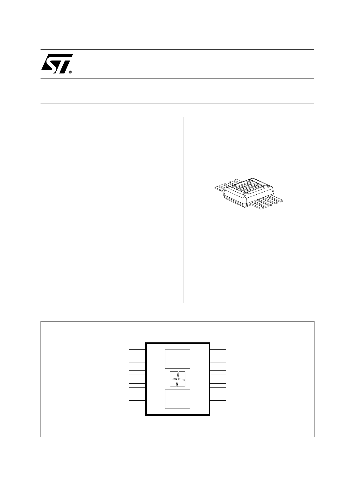
PHOTO DETECTOR FOR DIGITAL VIDEO DISK
.
LARGE BANDWIDTH (30MHz) AND LOW
NOISE I/U AMPLIFIER
.
SENSITIVITY SWITCHING FOR OPTICAL
PICKUPS
.
DETECTOR PATTERN ADAPTED FOR EFM
SIGNAL DETECTION, FOCUS AND TRACKING CONTROLS
DESCRIPTION
This six diodes photodetector includes six low
noise I/V amplifiers with a sensitivity switching for
adaptation to different optical pickups and disks.
The detector pattern is adapt able for astigmatism
focus method, 3 beams tracking and differential
phase detection methods.
The STV5805 is adapted for pick-up of DV D-ROM
and DVD players up to 3 x speed for both 1 layer
and 2 layer discs.
STV5805
PRELIMINARY DATA
OPTOSO10L
(Plastic Transparent Package)
ORDER CODE :
STV5805D
PIN CONNECTIONS
V
F
V
A
GAIN
V
B
V
E
June 1998
This is advance information on a new product now in development or undergoing evaluation. Details are subject to change without notice.
1
2
3
4
5
F
A
B
E
10
9
D
8
C
7
6
V
D
V
CC
V
O
GND
V
C
5805-01.EPS
1/5
Page 2
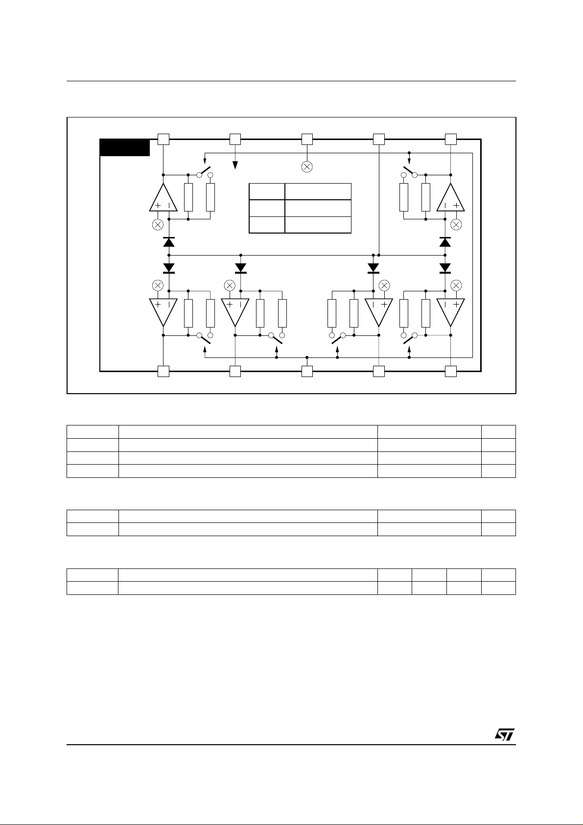
STV5805
BLOCK DIAGRAM
STV5805
V
D
D
F
V
CC
Mode
H Gain
L Gain
V
O
Voltage on Pin 3
V
CC
GND
GND V
AB
C
E
1 2 3 4 5
V
F
V
A
GAIN V
B
C
678910
V
E
5805-02.EPS
ABSOL UT E MAXIMUM RATINGS
Symbol Parameter Value Unit
V
CC
T
T
oper
Power Supply Voltage 6 V
Junction Temperature 150
j
Operating Temperature - 20, +70
THERMAL DATA
Symbol Parameter Value Unit
R
th (j-a)
Junction-ambient Thermal Resistance Max. 100
RECOMMENDED OPERATING CHARACTERISTICS
Symbol Parameter Min. Typ. Max. Unit
V
CC
Power Supply 4.75 5 5.25 V
o
o
o
C/W
C
C
5805-01.TBL
5805-02.TBL
5805-03.TBL
2/5
Page 3

STV5805
ELECTRICAL CHARACTERISTICS
(V
= 5V, VO = 2.5V , Light wavelength = 635 to 680nm, T
CC
Symbol Parameter Test Conditions Min. Typ. Max. Unit
I
SADH
SADL
SEFH
SEFL
BWAD
BWEF
DV0 Offset Voltage versus V
DVAB Offset Voltage (V
DVCD Offset Voltage (V
DVM Offset Voltage [(V
DVEF Offset Voltage (V
Supply Current Gain = H or L 25 mA
CC
Sensitivity A to D Gain = H
Gain = L
Sensitivity E, F Gain = H
Gain = L
Bandwidth at -3dB (A to D)
Bandwidth at -3dB (E, F)
0
- VB) Gain = H or L, in the dark -15 0 15 mV
A
- VD) Gain = H or L, in the dark -15 0 15 mV
C
+ VC) - (VB + VD)] Gain = H or L, in the dark -15 0 15 mV
A
- VF) Gain = H or L, in the dark -15 0 15 mV
E
Gain = H or L
Gain = H or L
Gain = H or L, in the dark -15 0 15 mV
Equivalent Noise Level (A to D) 10MHz, BW = 30kHz, in the dark
ENADH
ENADL
Gain = H
Gain = L
Equivalent Noise Level (E, F) 10MHz, BW = 30kHz, in the dark
ENEFH
ENEFL
I
VO
I
GAINH
I
GAINL
Input Current on V
O
Input Current on Gain Gain = V
Gain = H
Gain = L
VO = 2.5V 0.6 mA
Gain = GND
CC
= 25oC, unless otherwise specified)
amb
27
36
9
12
45
60
15
20
25
30
2
5
-74
-83
-62
-71
-1
+1
4515mV/µW
mV/µW
7535mV/µW
mV/µW
-66
-75
MHz
MHz
dBm
dBm
dBm
dBm
µ
A
µ
A
5805-04.TBL
Figure 1 :
Ty pical Spectral Sensitivity
1.0
0.8
0.6
0.4
0.2
RELATIVE SENSITIVITY
0
500 900600 700 800
WAVELENGTH (nm)
5805-03.EPS
3/5
Page 4

STV5805
DETECTOR PATTERN DIMENSIONS
190
250
(Position : Center of Package) (Unit : µm)
210 190
6°
150
DC
150
5
BA
5
light spot
EF
5805-04.EPS
4/5
Page 5

PACKAGE MECHANICAL DATA
10 PINS - PLA S TI C T R ANSP ARENT (OPT O )
STV5805
Information furnished is believed to be accurate and reliable. However, STMicroelectronics assumes no responsibility for the
consequences of use of such information nor for any infringement of patents or other rights of third parties which may result from
its use. No licence is granted by implication or otherwise under any patent or patent rights of STMicroelectronics. Specifications
mentioned in this publication are subject to change without notice. This publication supersedes and replaces all information
previously supplied. STMicroelectronics products are not authorized for use as critical components in life support devices or sys tem s
without express written approv al of STMi cr oelec troni cs.
2
Purchase of I
Rights to use these components in a I
Australia - Brazil - Canada - China - France - Germany - Italy - Japan - Korea - Malaysia - Malta - Morocco- The Netherlands
C Components of STMicroelectronics, conveys a license under the Philips I2C Pate n t .
Singapore - Spain - Sweden - Switzerland - Taiwan - Thailand - United Kingdom - U.S.A.
The ST logo is a trademark of STMicroele ct ronics
1998 STMicroelectronics - All Rights Reserved
©
2
2
C Standard Specifications as defined by Phili ps.
the I
STMicroelectronics GROUP OF COMPANIES
C system, is granted provided that the system conforms to
5/5
PMOPTO10.EPS
 Loading...