

Page 1

MULTISTANDARD ON-SCREEN DISPLAY
FOR VCR, PAY-TV, SATELLITE RECEIVER
.
A CHARACTER GENERATOR WITH ASCII
RAMAND CHARACTER ROM :
- 128characters
- 12 dots x 18lines character composition
- 11 rows x 28 characters pagecomposition
.
ACCURATE INTERNAL BANDGAP VOLTAGE
REFERENCE
.
LINE LOCKEDPLL
.
VIDEOTIMING GENERATOR
.
INPUT CVBS CLAMP AND SYNC EXTRACTOR
.
VERTICALSYNCSEPARATOR
.
INPUTCVBS SYNC RE-INSERTION
.
INPUTCVBS PRESENCEDETECTOR
.
PAL/NTSCCHROMAENCODER
.
DEDICATEDPINS FOR LUMAAND CHROMA
EXTERNALFILTERING
.
GAIN ON CVBS OUTPUT FOR EITHER 0dB
OR 6dB CAPABILITY
.
MULTISTANDARD TRANSLUCENT MIXED
MODE
.
OPAQUEMIXED MODE
.
NORMALFULLPAGEMODE
.
VIDEOFULL PAGE MODE
.
SUITABLEFOR S-VHS
.
THREE DIFFERENT MARKERS CAN BE
GENERATEDSIMULTANEOUSLY
.
THREE WIRE SERIAL INTERFACE FOR MICROPROCESSORCONTROL
DESCRIPTION
The STV5730AIC is intendedto be used in VCR,
Satellitereceiver andPAY-TV systemsfor CVBS or
R/G/Btext/graphicsinsertion.
(Plastic Micropackage)
ORDER CODE :STV5730A
PIN CONNECTIONS
YOUT
VIDEO IN
RES
FTR
AV
DV
CSYNC
XTAL IN
XTAL OUT
MUTE
DATA
CLK
CSN
DD
1
2
3
4
5
6
DD
7
8
9
10
11
12
13
14
R
STV5730A
SO28
28
YIN
27
VIDEO OUT1
26
VIDEO OUT2
25
CIN
24
COUT
23
LESCREEN
22
LECHAR
21
AGND
20
DGND
19
BAR
18
CO
17
FB
16
B
15
G
5730A-01.EPS
February 1996
1/20
Page 2

STV5730A
PIN DESCRIPTION
o
N
1 YOUT Analog Output This pin outputs the lumato allowthe user to notch filter it. This pin may be
2 VIDEO IN Analog Input This is the CVBS input. An external capacitor is needed for clamp operation.
3 RES Analog Pin it must be tied to an external resistor to control the PLL f0 frequency.
4 FTR Analog Pin itmust be tied to the line PLL loop filter.
5AV
6DV
7 CSYNC Bidirectional
8 XTAL IN DigitalInput This is the 4*fsc quartz input. The quartz may be started or stopped under
9 XTAL OUT Digital Output This is the 4*fsc quartz output. The quartz may be started or stopped under
10 MUTE DigitalOutput This pin indicates if the CVBS input signal is present on VIDEO IN input pin.
11 DATA Digital Input This is the serial interface data input.
12 CLK DigitalInput This is the serial interface clock input.
13 CSN Digital Input This is the serial interface chip select input.
14 R Digital Output This is the Red signal output. It is forced low during the horizontal and vertical
15 G Digital Output This is the Green signal output. It is forced low during the horizontal and
16 B Digital Output This is the Blue signal output. It is forced low during the horizontal and vertical
17 FB Digital Output This is the fast blanking output. It is delivered to control an external R/G/B
18 CO Digital Output This is the character activity output. It indicates if a character foreground is
19 BAR Digital Input This input forces the PLL in free run mode when active. It is enabled if the M0
20 DGND Supply Pin 0V digitalground.
21 AGND Supply Pin 0V analog ground.
22 LECHAR Analog Input This pin determines the characterintensity level in external bias mode (ie
23 LESCREEN Analog Input This pin determines the screen intensity level in external bias mode (ie when
24 COUT Analog Output This pinoutputs the fullpage mode chroma for external filtering (and
25 CIN Analog Input This pin inputs the filtered chroma.
26 VIDEO OUT2 Analog Output If the M7 mode bitis cleared : this pin is a CVBS output that delivers the
27 VIDEO OUT1 Analog Output This is a CVBS output.It delivers the VIDEO IN + text in mixed mode and the
28 YIN Analog Input This pin inputs the notch filtered luma.
Name Type Description
connected to the YIN input for minimum cost applications.
The STV5730A extracts the sync from this signal when the C7 controlbit is
set.
DD
DD
Supply Pin 5V analog supply pin.
Supply Pin 5V digital supply pin.
This pin inputs the mixed mode composite sync when the C7 control bit is
Pin
cleared.It outputs the video in extracted sync when the C7 control bit is set.
control of dedicated serial interface messages. Alternatively, a 4fsc clock can
be input directly. The stop message must not be used in this case.
control of dedicated serial interface messages.
It is forced low if the M2 mode bit is cleared.
blankingintervals.
vertical blanking intervals.
blankingintervals.
switch for R/G/B or TV applications.
beingdisplayed, andcan be used to control its intensity.
mode bit is set.
when the C10 control bit is set). This level must be defined relative to the
internal black reference. A variable luminance signal may be entered. To be
grounded if not used.
the C10 control bit is set). This level must be defined relative to the internal
black reference. A variable luminance signal may be entered. To be grounded
if not used.
attenuationif necessary). This pin may be connected to CIN for minimum cost
applications.
VIDEO IN signal. The sync is re-inserted if the M4 mode bit is set. The output
amplitude may be either 0dB or +6dB according to the M5 mode bit.
If the M7 mode bit is set : It outputs the currently active synchronism. The
signalamplitude is controlled by the M5 mode bit.
If the M8 mode bit is cleared : VIDEO OUT2 is in high impedance state.
CVBS text in full page mode. The output signal amplitude may be either 0dB
or 6dBaccording to the M5 mode bit. The sync is re inserted if the M4 mode
bit isset.
5730A-01.TBL
2/20
Page 3
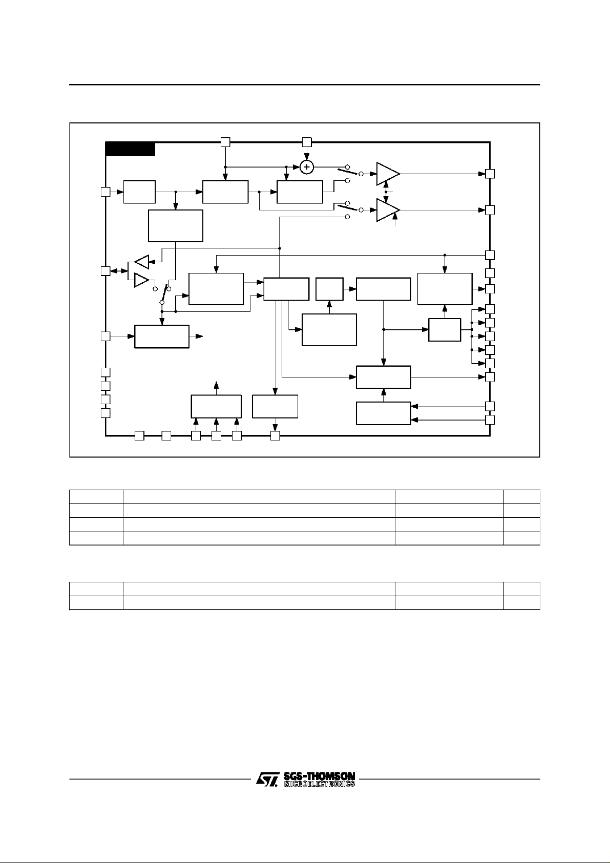
BLOCK DIAGRAM
STV5730A
VIDEO
2
CLAMP
7
19
5
6
21
20
LINE LOCKED
CS YNC
BAR
AV
DV
AGND
DGND
IN
DD
DD
COMPOSITE
SYNC
EXTRACTION
PLL
YIN CIN
28 25
SYNC
INSERTION
VERTICAL
SYNC
SEPARATION
PLXCLK
CONTROL
SERIALBUS
INTERFACE
11 1312 1043
INSERTION
H AND V
SCANNING
VIDEO
DETECTOR
MUTECSNCLKDATARESFTR
TEXT
GENERATOR
ASCII
RAM
RAM
ADDRESS
GAIN
DISABLE
CHARACTER
ROM
LUMA&SYNC
GENERATION
BIAS LEVEL
GENERATION
PAL/NTSC
ENCODER &
SATURATION
COLOR
LOGIC
STV5730A
VIDEO
27
OUT1
VIDEO
26
OUT2
XTAL
8
IN
XTAL
9
OUT
COUT
24
14
R
15
G
B
16
FB
17
CO
18
1
YOUT
LECHAR
22
LESCREEN
23
5730A-02.EPS
ABSOLUTEMAXIMUMRATINGS
Symbol Parameter Value Unit
DV
AV
DD
DD
T
Digital Supply Voltage 7 V
Analog Supply Voltage 7 V
Junction Temperature 150
j
THERMALDATA
Symbol Parameter Value Unit
R
th (j-a)
Junction-ambient Thermal Resistance Typ. 70
o
C/W
o
C
3/20
5730A-02.TBL
5730A-03.TBL
Page 4

STV5730A
ELECTRICAL CHARACTERISTICS (TA=0oCto 70oC, AVDD=DVDD= 5V,unless otherwisespecified)
Symbol Parameter Min. Typ. Max. Unit
DV
DD
DI
DD
AV
DD
AI
DD
AV
-DVDDAnalog to Digital Supply Voltage Difference -200 0 200 mV
DD
DV
OH
DV
DV
DV
DI
IH
DI
IL
BW Bandwidth at pins : VIDEO IN, VIDEO OUT1,
VIDEO IN (Pin 2)
V
SYNCIN
V
CL
C
IN
VIDEO OUT1(Pin 27)
V
OUT1
C
L1
R
L1
Z
OUT1
VIDEO OUT2(Pin 26)
V
OUT2
C
L2
R
L2
Z
OUT2
GAIN (Pins 26- 27)
CIN (Pin 25)
C
CIN
R
CIN
YIN (Pin 28)
C
YIN
YOUT (Pin 1)
V
YOUT
C
LYOUT
R
LYOUT
COUT (Pin 24)
V
COUT
C
LCOUT
R
LCOUT
Digital Supply Voltage DVDD- DGND 4.75 5.0 5.25 V
Digital Supply Current 10 mA
Analog Supply Voltage 4.75 5.0 5.25 V
Analog Supply Current 25 mA
Digital Output Voltage High Level (I
Digital Output Voltage Low Level (I
OL
Digital Input Voltage High Level 0.75 x
IH
Digital Input Voltage Low Level 0.15 x
IL
= -1mA) DVDD-0.5 V
LOAD
= +1mA) DGND + 0.5 V
LOAD
- DGND)
(DV
DD
(DV
DD
Digital Input Current High Level 1 µA
Digital Input Current Low Level -1 µA
8.0 MHz
VIDEO OUT2, CIN, YIN, YOUT, COUT
Sync Pulse Range 100 650 mV
Clamp Voltage 1.10 1.30 1.50 V
External Capacitor 2.2 µF
Output Dynamic Range 2.0 4.4 V
Black Level Voltage 2.20 2.45 2.70 V
Output Capacitor Load 20 pF
Output Resistor Load 10 kΩ
Output Impedance 250 Ω
Output Dynamic Range 2.0 4.4 V
Black Level Voltage 2.20 2.45 2.70 V
Output Capacitor Load 20 pF
Output Resistor Load 10 kΩ
Output Impedance 250 Ω
Gain Dispersion 0dB
6dB
-1
5
0
6
Input Capacitance 0.5 pF
Input Resistance 50 kΩ
Input Capacitance 0.5 pF
Output Dynamic Range 0.5 3.5 V
Output Capacitor Load 15 pF
Output Resistor Load 10 kΩ
Output Dynamic Range 0.5 3.5 V
Output Capacitor Load 15 pF
Output Resistor Load 10 kΩ
- DGND)
+1
7
V
V
dB
dB
5730A-04.TBL
4/20
Page 5

STV5730A
ELECTRICAL CHARACTERISTICS
=0oCto70oC, AVDD=DVDD=5V, unless otherwisespecified) (continued)
(T
A
Symbol Parameter Min. Typ. Max. Unit
LESCREEN (Pin 23)
V
LESCR
LECHAR (Pin 22)
V
LECH
INTERNAL SIGNAL LEVELS (Pins 1- 24)
V
SYNC
V
BLACK
V
SCREEN
V
CHAR
∆V1 Difference Level between Black and Sync Level 250 300 350 mV
∆V2 Difference Level between Screen and Black Level 100 150 200 mV
∆V3 Difference Level between Char. and Screen Level 450 515 580 mV
V
BURSTPP
V
CH1PP
V
CH2PP
BUS (Pins 11- 12 - 13)
f
CLK
t
CWL
t
CWH
t
CSWL
t
CSWH
t
DCLH
t
CLD
t
CLCSL
t
CSLCLL
t
CLHCSH
t
CSHCL
* maxHZ is the maximum horizontal zoom factor that is used
InputLevel 1.0 3.0 V
InputLevel 1.0 3.0 V
Internal Sync Level 0.95 V
Internal Black Level 1.1 1.25 1.4 V
Internal LESCREEN 1.4 V
Internal LECHAR 1.9 V
Burst Amplitude 320 mV
Chroma Amplitude for blue or yellow colors
for red, magenta, green or cyan colors
420
580
CLK Frequency Range 0 2 MHz
CLK Width Low 200 ns
CLK Width High 200 ns
CSN Width Low maxHZ* x 4 µs
CSN Width High maxHZ* x 4 µs
DATA Valid to CLK High 100 ns
CLK High to DATA Unvalid 100 ns
CLK Valid to CSN Low 100 ns
CSN Low to CLK Low 100 ns
CLK High to CSN High 100 ns
CSN High to CLK Unvalid 100 ns
mV
mV
PP
PP
PP
5730A-05.TBL
Figure1
DATA
CLK
t
CLCSL
CSN
t
DCLH
t
CSLCLL
t
t
CLD
t
CSHCL
t
CWL
t
CSWL
t
CWH
t
CLHCSH
t
CSWH
CLCSL
5730A-03.EPS
5/20
Page 6

STV5730A
TYPICAL PAL/NTSC/SECAM APPLICATION
CVBS OUT
Ω
68
Ω
180
+5V
(see Note 1)
CHROMA BP FILTER
EXTERNAL
RGB
TEXT
INSERTION
Ω
68
(SCART)
+5V
Ω
68
Ω
180
+5V
+5V
+5V
Ω
180
68Ω
(see Note 3)
R1
+5V
Ω
Ω
180
68
CHROMA TRAP
20
9
220nF
+5V
17
18
19
0
A
10
11
12
39pF
Ω
180
15
16
13
14
39pF
TRANSLUCENT MODE
21
22
23
24
25
26
27
28
6
573
7
220nF
8
STV
LUMAFILTER (see Note 1)
F
µ
2.2
1
2
3
4
5
Ω
4.3k
H
µ
10
CVBS IN
(see note 4)
220pF
Notes : 1. Optional filter.For low cost applications, short circuit.
2. The 4fsc (17.734MHz PAL,14.318MHz NTSC) crystal may be ommited if this signal is already available in a system.
3. External bias level can be set by resistor ratio as required. The level atpins LECHAR and LESCREENmust not exceed 3.0 Vdc.
4. Output impedance of the driving stage should be less than 300Ω.
22kΩ
22nF
+5V
CSYNC
(INor OUT)
Ext. 4 fsc
XTAL
x 4fsc
OSC IN
(see Note 2)
TO MICRO
6/20
Digital Ground
Analog Ground
5730A-04.EPS
Page 7

FUNCTIONAL DESCRIPTION
The STV5730Aoperates in ”mixed mode” or ”full
page mode” :
- Mixed mode : the device is line locked to the
incomingCVBS signal.The textissuperimposed
overthe CVBSinputeitherinB&Wortranslucent.
It mayalsobesuperimposedincolorbyusingthe
R/G/Boutputs.
- Full pagemode : the device generatesa colored
PAL or NTSC CVBS output and simultaneous
R/G/B outputs. Both ”normal full page” and
”video full page” modes are supported by the
STV5730A.In the ”normal full page” the screen
background is uniformely colored, while the
”video full page” mode permits to display the
unlocked VIDEO IN signal in the screen backgroundarea.
It performs the followingtext features:
- Page composition: 11rows X 28 characters
- Number of displayed characters: 308 (max)
- Character composition: 12 dots X 18 lines
- ROMcharac terset : 128 userdefina blecharacters
STV5730A
- Screendisplaypositions:58horizontalpositions,
63 vertical positions
- Rowpositionoffset , eachrow : Xoffsetfrom 0 to
+15,Yoffsetfrom -17 to +17
- Display enable : each row or page
- Charactercolor : 1 out of 8, each character
- Characterbackgroundcolor : 1 outof 8, characterandpage enabledorsetidenticalto character
color
- Characterborder color : 1 out of 8, row enabled
or set identical to character color
- Pagebackgroundcolor : 1 out of 8
- Zoom: 3 independant zoom factors for rows 0,
1 to 9 and 10.
- Zoom factors : four independant X and Y zoom
factors
- Blink: character and page enabled
- Blinkfrequency: 0.5 or 1.0 second
- Blinkduty cycle : 0.25, 0.5 or 0.75
1 - THE INTERNAL RAM BUFFER
It stores the page (i.e.the text definition)and the row attributes.
1.1 - Page
The page includes 11 row buffers, numbered from 0 to 10. Each row buffer includes 28 characters,
numbered from 0 to 27. The characters may be written one by one by the microprocessor for random
access.They also may be written sequentially,startingwith any characteraddress.
1.2 - CharacterFormat and Attributes
11 10 9 8 7 6 0
BE R G B BK CHARACTER CODE
CHARACTER CODE : 1 character out of 128 from the characterROM
BK : BK=0 : character blink disabled
BK=1 : characterblink enabled
R/G/B : Charactercolor:
BE : BE=0 :
BE=1 :
000
001
010
011
100
101
110
111
the character background is disabled
the character backgroundis enabled
black
blue
green
cyan
red
magenta
yellow
white
7/20
Page 8

STV5730A
FUNCTIONAL DESCRIPTION (continued)
1.3 - Row Attributes
Thereare 11 row attributes, numberedfrom 0 to 10. Theymay be writtenone by one or sequentially.
The row attributeformat is as follows :
11 8765 0
HPOS OFFSET RE FBE VPOS OFFSET
VPOS OFFSET : the MSBis the sign bit (0 : positive,1 : negative).If theoffsetispositive(from0 to+17),
then the correspondingnumber of lines are added on top of the row (i.e. it moves
downwards). These extra lines are colored according to the character background
rules. If the offset is negative(from -1 to -17),then the correspondingnumberof lines
are subtractedfrom the display of the row.
FBE : FBE=0 : the characters are displayed withoutborder
FBE=1: the characters are displayedwith border
RE : RE=0 :
RE=1 :
HPOSOFFSET : The display of the row is shifted to the right by the correspondingnumber of pixels
(from0 to 15).
1.4 - The Control Registers
Thereare 5 registers for microprocessorcontrol.They can be writtenindividuallyor sequentially:
- the ZOOMregister address : 12
- the COLORregister 13
- the CONTROLregister 14
- the POSITIONregister 15
- the MODEregister 16
the charactersof the roware not displayed.
They are replaced by the page backgroundcolor.
the charactersof the roware displayed.
1.4.1 - Zoom Register
11109876543210
VZb1 VZb0 HZb1 HZb0 VZm1 VZm0 HZm1 HZm0 VZt1 VZt0 HZt1 HZt0
HZt[1:0] : Toprow horizontalzoom factor (ie row 0)
HZt[1:0] = 00
:
1 pixel per character dot
01
:
2 pixels per characterdot
10
:
3 pixels per characterdot
11
:
4 pixels per characterdot
VZt[1:0] : Top row vertical zoom factor
VZt[1:0] = 00
:
1 pixel per character line
01
:
2 pixels per characterline
10
:
3 pixels per characterline
11
:
4 pixels per characterline
HZm[1:0] : Same as HZt[1:0], for middlerows (ie rows 1 to 9)
VZm[1:0] : Same as VZt[1:0],formiddle rows
HZb[1:0] : Same as HZt[1:0], for bottom row(ie row 10)
VZb[1:0] : Same as VZt[1:0],forbottom row
The outputof thisregister issynchronizedby thehorizontalsynchronism.The RESETmessageclearsthis
register.
8/20
Page 9

STV5730A
FUNCTIONAL DESCRIPTION (continued)
1.4.2 - Color Register (pageattributes)
11109876 210
R G B R G B // // // R G B
SBC FBC BCC
SBC : screen background color
FBC : character border color
BCC : characterbackground color
The output of thisregister is synchronizedby the horizontalsynchronism.
1.4.3 - ControlRegister
11109876543210
C11 C10 C9 C8 C7 C6 C5 C4 C3 C2 C1 C0
C0 : C0 = 0 : mixed mode
C0 = 1 : full page mode
C1 : C1 = 0 : the character backgroundis controlled by BE (see character word description)
C1 = 1 : all displayedcharacter backgrounds are disabled
C2 : C2 = 0 : display off
C2 = 1 : display on
C3 : C3 = 0 : the characters are colored according to the character attribute and the color register
values(i.e. CBACKGand CBORD)
C3 = 1 : the character foreground,border and background colors are all set to the character
attributevalue(see paragraph1.2). This optionis mainly intended for full page mode,
CVBSor Y/C output
C4 : C4 = 0 : 1.0 second blinking period
C4 = 1 : 0.5 second blinking period
C[6:5] : C[6:5] = 00
C7 : C7 = 0
C7 = 1
C8 : C8 = 0 : the standard is NTSC, 60Hz
C8 = 1 : the standard is PALor SECAM with M6 = 0, 50Hz
C9 : C9 = 0 : character colorencoding is disabled
C9 = 1 : character colorencoding is enabled
C10 : C10 = 0 : theluminance levels are generated internally
C10 = 1 : the luminance levels are provided by the LESCREENand LECHARinput pins.
C11 : C11 = 0 : VideoFull Page Mode. A stable full page modetext is displayedwhile the screen
C11= 1 : Normalfull page mode is active.
The outputof thisregister issynchronizedby thehorizontalsync(exceptC7).The RESETmessageclears
this register.
:
blinkingoff
01
:
0.75blinking duty cycle
10
:
0.5 blinking duty cycle
11
:
0.25blinking duty cycle
an external input compositesync is taken from the CSYNC pin
the sync is extracted by the STV5730A.The currently active sync is output on the
CSYNCpin
background is the unlocked video input signal.
9/20
Page 10

STV5730A
FUNCTIONAL DESCRIPTION (continued)
1.4.4 - PositionRegister
11 6 5 0
VERTICAL POSITION HORIZONTAL POSITION
HORIZONTAL POSITION Any value from 6 to 63
VERTICALPOSITION Any value from1 to 63
1.4.5 - Mode Register
11109876543210
M11 M10 M9 M8 M7 M6 M5 M4 M3 M2 M1 M0
M0 : M0 = 0
M0 = 1::
M1 : M1 = 0
M1 = 1::
M2 : M2 = 0
M2 = 1::
M3 : M3 = 0
M3 = 1::
M4 : M4 = 0
M4 = 1::
M5 : M5 = 0
M5 = 1::
M6 : M6 = 0
M6 = 1::
M7 : M7 = 0
M7 = 1::
M8 : M8 = 0
M8 = 1::
M9 : M9 = 0
M9 = 1::
M10 : M10 = 0
M10 = 1::
M11 : M11 = 0
M11= 1::
Note : This mode overides the normal functions of Pins CSYNC and BAR.
the BAR pin is disabled
the BAR pin has an actionon theline PLL
the missing sync pulses are not detected
the missing sync pulses are detected
the MUTE pin is forced to 0
the MUTE pin deliverstheinternal MUTE signal
the MUTE time constantis 8lines
the MUTE time constantis 32lines
the sync is not re-inserted
the sync is re-insertedfor improved text stability
the gain of pins VIDEO OUT1 & VIDEO OUT2 is 0dB.
the gain of pins VIDEO OUT1 & VIDEO OUT2 is 6dB.
the color encoderis enabled (PALor NTSC)
the color encoderis disabled(B&W or SECAM)
the VIDEO OUT2 pin outputstheVIDEO IN signal
the VIDEO OUT2 pin outputsthecomposite sync
the VIDEO OUT2 pin is in low impedancestate
the VIDEO OUT2 pin is in high impedance state
Normalmode
CSYNCPin outputs the burstgate,BAR Pin outputs the VSYNC (see Note)
No delay compensation
It enablesthe delay compensationof the internal sync extractor.
The mute signal output is synchronizedon vertical syncin order to limit its transitions.
The mute signal is not synchronizedon vertical sync thus accelerating the VIDEO IN
presencedetection (useful in full page mode).
10/20
Page 11

STV5730A
FUNCTIONAL DESCRIPTION (continued)
2 - THE MICROPROCESSORSERIALINTERFACE
The STV5730Ais down loaded by the microprocessor througha threewire serial interface : DATA,CLK,
CSN. The CLK and CSN signals are internallyORed in orderto validatethe transferwhen the STV5730A
is chipselected only (i.e. CSN = 0). The CSN risingedge validates the internal data transfer.
2.1 - Message Formats (see Figure 2)
16-bit, 8-bit and 0-bit formats are available.The 8-bit and 0-bit message formatsmay be usefulto speed
up the STV5730Adown loading.
15 1211 87654 0
0000 BUF[11:8] STRU[7:6] 0 DEPL[4:0] ADDRESS
This16-bitaddressmessageloadstheserial interfacewritepointer.Thisaddressis incrementedafter each
data message.
15 12 11 0
0001 DATA[11:0] DATA
This 16-bit data message writes the data at the locationindicated by the writepointer.
70
DATA[7:0] DATA
This 8-bitdata messagewrites the data at the locationindicated by the writepointer. The 4-bit data MSB
is copied from the last previous 16-bit data message.
The 0-bit data message writes a data at the location indicated by the write pointer. The last data is used
fromthe previous8-bit or 16-bit data message.
15 12 11 0
0010 don’tcare CONTROL
This 16-bit control messagestops the 4*fsc quartz oscillator.
15 12 11 0
0011 don’tcare CONTROL
This 16-bit control message resets the circuit and startsthe 4*fscquartz oscillator. This message should
not be usedif an external4 x fsc clock is used instead of the quartz. It is mandatorythat reset operation is
as described in paragraph 2.3.
11/20
Page 12

STV5730A
FUNCTIONAL DESCRIPTION (continued)
Figure2
15 14 13 12 2 1 0
DATA
CLK
CSN
76543210
DATA
CLK
CSN
DATA
CLK
CSN
2.2 - The WritePointer
As described in the ”messageformat” paragraph,
an address consists of three fields : STRU[7:6],
BUF[11:8], DEPL[4:0].
mentedaftereachdatamessage.When thewrite
of a row is completed, the writepointer is automaticallyset to the next row first character.
- STRU[7:6] = 01 :
The STRU[7:6] fieldindicateswhether it isa PAGE
address or a ROW ATTRIBUTE / REGISTER ad-
dress. It also determinesthe address incrementation scheme.
- STRU[7:6] = 00 :
It is a PAGE address. BUF provides the row
number (from 0 to 10) and DEPL provides the
character number (from 0 to 27). DEPL is incre-
It isalso a PAGEaddressbut the incrementation
schemeisa bitdifferent: whenthe writeof a row
is completed, the write pointer is automatically
set to the firstcharacter of the same row.
- STRU[7:6] = 11 :
Itisarow attributeor aregisteraddress.The BUF
field must be set to 0000 and the DEPL field is
incrementedaftereach data access.
2.2.1 - Address Map
PAGE : ROW 0 : STRU[7:6]= 0 or 1 - BUF[11:8]= 0 - DEPL[4:0]from 0 to 27
ROW1 : STRU[7:6]= 0 or 1 - BUF[11:8]= 1 - DEPL[4:0]from 0 to 27
......... : ................. ..................... ................
ROW10 : STRU[7:6]= 0 or 1 - BUF[11:8] = 10 - DEPL[3:0]from 0 t0 27
ROWATTRIBUTES : STRU[7:6]= 11 - BUF[11:8]= 0 - DEPL[4:0]from 0 to 10
REGISTERS : STRU[7:6] = 11 - BUF[11:8] =0
DEPL[4:0]= 12 for ZOOM register,13 forCOLOR register,
14 for CONTROLregister, 15 forPOSITION register,
16 for MODE register
16-BIT
MESSAGE
8-BIT
MESSAGE
0-BIT
MESSAGE
5730A-05.EPS
12/20
Page 13

FUNCTIONAL DESCRIPTION (continued)
2.3 - Initializationand Down-loadingSequence
It is importantthat theSTV5730Ais correctlyreset
and initialized after the circuit is powered prior to
anywriting. This routine is shown in Figure 3. The
two initialization bytes (00db 1000) must procede
theresetinstruction(x2)everytimeitistransmitted.
Figure3
RESET & INITIALIZE
3000H
3000H
00dbH
1000H
Set Control Registers
* Zoom
* Color
* Control
* Position
* Mode
Set Row Attributes
* 0 to 10
STV5730A
TheSTV5730APLLis alsoinsensitiveto the head
switching disturbingthe synchronisminVTR applications (playback).
The missing pulses may be detected. The M1
modebit enablesthe detection.
In addition, the BAR input pin is available to enter
a signal that forces the PLL in free-run mode. This
capability may be used for search mode in VTRs,
to improve the loop robustness against the noise
bar.TheBAR inputis enabledby the M0 mode bit.
3.2 - HorizontalSyncRe-insertion
This mechanism is of interest in mixed mode, to
cancelthetexthorizontaljitterwhenthesyncsignal
is too bad. It is activated by the M4 mode bit and
must be turned off in full page mode.
The active part of the line is protected against
parasiticsyncinsertion.Themodifiedsyncis active
on all output pins (ie CSYNC if C7 is set, VIDEO
OUT1, VIDEO OUT2).
Ajitter greater than 0.42useccannotbe cancelled.
3.3 - Full Page Mode Behavior
Inthiscase,thePLLislockedon an internal64usec
referencederivedfrom the 4*fsc quartz.
TheSTV5730Ageneratesa non interlaceoutput.
Set RAM Attributes
i.e. TEXT PAGE
* Write Pointer
* Data
* etc.
Next Page
Write
STOP
3 - THE LINE LOCKED PLL
The PLLfrequencyis 504 * f
=7.875MHz.
H
3.1 - Mixed Mode Behavior
In mixedmode,the internalPLLis linelockedtothe
incomingCVBSsignal.The syncis eitherextracted
by the STV5730A(if C7 control bit is set) or provided bythe applicationin acompositeformon the
CSYNC pin (if C7 control bit is cleared). The
STV5730A separates the vertical sync from the
compositesynchronism.
The STV5730A PLL features built-in protection
mechanismsagainstmissingandparasitichorizontal sync pulses. These mechanisms are activated
when the loop is locked.
4 - MUTE
The STV5730A monitors the sync to determine
whetherit is a stable signal or not.
MUTE =high : no stable signal
MUTE =low : stable CVBSinput signal
The MUTE search time constant may be either
8 lines or 32 lines, accordingto the M3 mode bit.
Thesignalthat is deliveredto the MUTE outputpin
is synchronized on the vertical sync if M11 is
5730A-14.EPS
cleared. It is forced low if the M2 mode bit is low.
This signal maybe monitoredby the microprocessor to switch the STV5730A from mixed mode to
fullpage mode and viceversa(usingtheC0 control
bit).
5 - THE LUMA GENERATOR
The luma signal is generated by the STV5730A
from timing information created by the character
and video timing generators and voltage levels
created by the internal bias level generator or
enteredon the LESCREENand LECHARpins (as
selectedby the C10 control bit).
Theluma signalis outputon the YOUTpinto allow
the user to notch filter it. It is then re-input on the
YINpin.YOUTandYINmaybe connectedtogether
for minimal cost applications.
13/20
Page 14

STV5730A
FUNCTIONAL DESCRIPTION (continued)
5.1 - Internal Bias Mode
This mode is intended for minimal cost applications. C10 must be cleared.
The luma levels of the OSD output signal are as
follows :
- LEBLACK : black level
nominalvalue : 1.25V
- LESYNC : sync level
nominalvalue : LEBLACK- 300mV
- LESCREEN : pagebackgroundlevel
nominalvalue : LEBLACK+ 150mV
- LECHAR : characterlevel
nominalvalue : LEBLACK+ 650mV
LEBLACK is also used to clamp the VIDEO IN
signaland to create the characterborder.
5.2 - External Bias Mode
This mode is intended to give more flexibilityto the
user.C10 must be set.
The LESCREEN and LECHARlevels may be user
defined relatively to the internalLEBLACKlevel.
Thefinallumaamplitudeshouldnotbegreaterthan
the peak white level.
Theselevels may be static or dynamic.
Dynamiclevelscan be easily generated by analog
sum of the R/G/B and CO STV5730A outputs (a
few resistors are necessary) to give grey scale
charactershading in the mixed mode.
C0 is useful to control the character foreground
lumalevel.
6 - THE CHROMA GENERATOR
TheSTV5730Aencoderoperatesinfullpagemode
only.ItmayperformPALorNTSCencodingaccording to the C8 control bit.
A 4*fsc chroma quartz crystal is necessary
(fsc =4.43MHz for PAL,3.58MHz for NTSC).
The encodercan be turned off by the M6 mode bit
for black & white or for SECAMapplications.
The character encoding is controlled by the C9
controlbit.
The chroma signal is output on the COUT pin for
externalfilteringand for attenuationif necessary.It
is thenre-entered on the CIN pin and added to the
YIN pin signal to create the final CVBS output
signal.
The chroma saturation is controlled by the
STV5730A:
- burst nominal amplitude: 320mV
- blue or yellow colors nominal amplitude :
420mV
PP
- red, magenta,green or cyan colorsnominalam-
plitude: 580mV
PP
PP
7 - THE MARKERS
The STV5730Acan generate 3 different markers
that can be activated simultaneously (i.e. on the
samepage).
The followingmarker features are performed:
- Blinking character,characterbackground off.
Thecharacter foregroundblinks (BK= 1, BE= 0
or C1 = 1).
- Not blinkingcharacter,characterbackgroundon
(C1 = 0, BE = 1).
- Blinking character,characterbackground on.
Thecharacter foregroundblinks and the characterbackgroundremains(BK= 1, BE=1, C1=0).
8 - THE TRANSLUCENT MIXED MODE
Figure4 : TheTranslucent Mixed Mode Output
Configuration
1
R1
S
R2
28
disable
VIDEO OUT1
VIDEO OUT2
STV5730A
The VIDEOOUT1 and VIDEOOUT2 outputs may
be summed via two external resistors to create a
translucent text (mixed mode). In this case, the
backgroundpictureis still visible behind the text.
The background picture visibility (or level of translucenceis controlled by the resistorratio.
Another benefit from this function is to allow
PAL/SECAM/NTSC multistandard applications to
be built with no SECAM chroma re-insertion filter
and no additional controlswitches.
The summay becancelledbysettingthe M8mode
bit. In this case, the VIDEO OUT2 pin is in high
impedancestate and the resistor networkdelivers
VIDEOOUT1 only.
Whenusing the resistor network, please set M8 in
the following cases :
- in full page mode
- when OSDin not displayed
- to select opaque text. This allows the viewer to
select by softwarethe preferreddisplay mode.
The DC levels of theVIDEO OUT1, VIDEO OUT2
and the sum signals are high enough to directly
drive a NPN emitter followerdriver (see Table 1).
5730A-06.EPS
14/20
Page 15

STV5730A
FUNCTIONAL DESCRIPTION (continued)
9 - VIDEO FULL PAGE MODE
In additionto thenormal full page mode in which a
uniformely colored screen background is generated, theSTV5730Ais able to performa ”video full
page mode”.
Normal and video full page mode are selectedby
the control bit C11(respectively set high and low).
By using the video full page mode the channel
capture operation can be easily monitored on the
screen since the signal at the VIDEO IN input is
displayed, unlocked, in the screen background
area ; the text being stable and colored, with or
withoutcolored background.
Presencedetection is permanently active to keep
the microcontroller informed of the input signal
quality. The information is delivered by the MUTE
pin.
Thisinformationcan beusedbythemicrocontroller
to force the STV5730A into the mixed mode (set
C0 low) when the input signal becomes good
enough.
Table1
FULL PAGE
PAL/NTSC
VIDEO OUT1 CVBS (OSD) VIDEO IN or Text VIDEO IN or Text
VIDEO OUT2 High impedance VIDEO IN High Impedance
S CVBS
(OSD)
TRANSLUCENT PAL/NTSC/SECAM OPAQUE PAL/NTSC
x Text + R1x VIDEO IN
R
2
In the video full pagemode, it canbe usefull to set
the M11(mode register)bit high, so that the mute
signalisnotsynchronizedonthe verticalsync,thus
acceleratingthe VIDEO IN presence detection.
10 -S-VHS APPLICATION (see Figure 5)
The STV5730Acan be used inS-VHSapplications
easily.
The Y signal must be delivered to the VIDEO IN
input. The VIDEO OUT1 output then delivers a
Y +textsignal,whilstthe VIDEOOUT2deliversthe
Y input signal, provided that the CIN input is connected to a bias DC level.
An external switch must be used to select the C
signalin mixedmode or the COUToutput signal in
full page mode.
In mixedmodethe chromasignal(C)can be externally attenuated (multistandard translucentoperation) or killed (PAL/NTSC opaque operation only)
during the character gate controlled by the fast
blankingsignal.
MIXED MODE
VIDEO IN or
R
+ R
1
2
VIDEO IN
or Text
Figure 5 : S-VHSInput/OutputConfiguration
STV5730A
Y
INTERNALBIAS
VIDEO IN VIDEO OUT1
VIDEO OUT2
CIN
FB
15
C
CHARACTER
GATED
ATTENUATOR
12
28
COUTFP2223
R
1
R
2
OP TIONAL
FILTER
Y
OSD
Yor Text
R
Text R
2
Yor
*
R
1
EXTERNAL
MM
SWITCH
Mixed Mode (MM)
Full Page Mode (FP)
Fullpage mode
Opaque mixed mode
Y
1
*
R
2
Transluce nt mixed mode
C
5730A-07.EPS
15/20
Page 16

STV5730A
FUNCTIONAL DESCRIPTION (continued)
11- THE CVBS OUTPUTPICTURE
The following tables show the picture design in CVBS output mode (VIDEOout1 analog output pin)
accordingto :
- Blink on/off (BK character attribute& C[6:5] controlbits)
- Character backgroundon/off (BE characterattribute & C1 control bit)
- Character border on/off (FBE row attribute)
11.1- Mixed Mode
CHARACTER
FOREGROUND
Not Blinking and
Char Backg off
Not Blinking and
Char Backg on
Blinking and Char Backg off video
Blinking and Char Backg on LESCREEN video
LECHAR LEBLACK video
LECHAR LEBLACK LESCREEN video
11.2- Full Page Mode
CHARACTER
FOREGROUND
Not Blinking and
Char Backg off
Not Blinking and
Char Backg on
Blinking and Char Backg off LESCREEN + CSCREEN
Blinking and Char Backg on LESCREEN + CBACKG LESCREEN +
LECHAR +
CCHAR
LECHAR +
CCHAR
CCHARis a character attribute.
C3 = 0 : CSCREEN, CBACKGand CBORD are page attributes, defined by the color register.
C3 = 1 : CSCREEN is defined by the color register. CBACKG and CBORD are identical to CCHAR and
thus are character attributes.
CHARACTER
BORDER
if on
CHARACTER
BORDER
if on
LEBLACK +
CBORD
LEBLACK +
CBORD
CHARACTER
BORDER
if off
CHARACTER
BORDER
if off
LESCREEN + CBACKG LESCREEN +
CHARACTER
BACKGROUND
CHARACTER
BACKGROUND
LESCREEN + CSCREEN
BACKGROUND
BACKGROUND
CSCREEN
CSCREEN
PAGE
PAGE
16/20
Page 17

STV5730A
FUNCTIONAL DESCRIPTION (continued)
12 - THE R/G/B OUTPUT PICTURE
The followingtables show the picture design in R/G/B output mode, accordingto :
- Blink on/off (BK character attribute& C[6:4] controlbits)
- Character backgroundon/off (BE characterattribute & C1 control bit)
- Character border on/off (FBE row attribute)
- C3 = 0 : CSCREEN, CBACKGand CBORD are page attributes, definedby the colorregister.
- C3 = 1 : CSCREEN is definedby the colorregister.CBACKGand CBORDare identicalto CCHAR and
thus are character attributes. It is recommended to use CO output signalin this case.
AnR/G/Bexternalswitchmustbe controlledbythe STV5730AFBoutputto performthecharacterinsertion.
C0 may be usedas an additionalcharacter intensity signal.
12.1 - Mixed Mode
CHARACTER
FOREGROUND
Not Blinking and
Char Backg off
Not Blinking and
Char Backg on
Blinking and Char Backg off video
Blinking and Char Backg on CBACKG video
CCHAR CBORD video
CCHAR CBORD CBACKG video
CHARACTER
BORDER
if on
CHARACTER
BORDER
if off
CHARACTER
BACKGROUND
PAGE
BACKGROUND
12.2 - Full Page Mode
CHARACTER
FOREGROUND
Not Blinking and
Char Backg off
Not Blinking and
Char Backg on
Blinking and Char Backg off CSCREEN
Blinking and Char Backg on CBACKG CSCREEN
CCHAR CBORD CSCREEN
CCHAR CBORD CBACKG CSCREEN
CHARACTER
BORDER
if on
CHARACTER
BORDER
if off
CHARACTER
BACKGROUND
PAGE
BACKGROUND
CCHARis a character attribute.
C3 = 0 : CSCREEN, CBACKGand CBORD are page attributes, defined by the color register.
C3 = 1 : CSCREEN is defined by the color register. CBACKG and CBORD are identical to CCHAR and
thus are character attributes.
17/20
Page 18

STV5730A
FUNCTIONAL DESCRIPTION (continued)
13 - STANDARDCHARACTERS
The defaultdevice is deliveredwith a standardset of ROM based characters(see Figure 6).
The user can redefine the total characterset (except for the character 00H (zero)).
Figure6
00H 01H 02H 03H 04H 05H 06H 07H
08H 09H 0AH 0BH 0CH 0DH 0EH 0FH
10H 11H 12H 13H 14H 15H 16H 17H
18H 19H 1AH 1BH 1CH 1DH 1EH 1FH
20H 21H 22H 23H 24H 25H 26H 27H
28H 29H 2AH 2BH 2CH 2DH 2EH 2FH
30H 31H 32H 33H 34H 35H 36H 37H
38H 39H 3AH 3BH 3CH 3DH 3EH 3FH
5730A-12.EPS
18/20
Page 19

FUNCTIONAL DESCRIPTION (continued)
13 - STANDARDCHARACTERS (continued)
Figure6 (continued)
40H 41H 42H 43H 44H 45H 46H 47H
48H 49H 4AH 4BH 4CH 4DH 4EH 4FH
50H 51H 52H 53H 54H 55H 56H 57H
58H 59H 5AH 5BH 5CH 5DH 5EH 5FH
STV5730A
60H 61H 62H 63H 64H 65H 66H 67H
68H 69H 6AH 6BH 6CH 6DH 6EH 6FH
70H 71H 72H 73H 74H 75H 76H 77H
78H 79H 7AH 7BH 7CH 7DH 7EH 7FH
5730A-13.EPS
19/20
Page 20

STV5730A
PACKAGEMECHANICAL DATA
28 PINS- PLASTICMICROPACKAGE
PM-SO28.EPS
Dimensions
Min. Typ. Max. Min. Typ. Max.
Millimeters Inches
A 2.65 0.104
a1 0.1 0.3 0.004 0.012
b 0.35 0.49 0.014 0.019
b1 0.23 0.32 0.009 0.013
C 0.5 0.020
c1 45
o
(Typ.)
D 17.7 18.1 0.697 0.713
E 10 10.65 0.394 0.419
e 1.27 0.050
e3 16.51 0.65
F 7.4 7.6 0.291 0.299
L 0.4 1.27 0.016 0.050
S8
Information furnished is believed tobe accurate and reliable. However,SGS-THOMSON Microelectronics assumes no responsibility
for the consequences of use of such information nor for any infringement of patents or other rights of third parties which may result
from its use. No licence is granted by implication or otherwiseunder anypatent or patent rights of SGS-THOMSON Microelectronics.
Specifications mentioned in this publication are subject to change without notice. This publication supersedes and replaces all
information previously supplied. SGS-THOMSON Microelectronics products are not authorized for use as critical componentsin life
support devices or systems withoutexpress written approval of SGS-THOMSON Microelectronics.
1996 SGS-THOMSON Microelectronics - All Rights Reserved
Purchase of I
2
I
C Patent. Rights to use these components in a I2C system,is granted provided that the system conforms to
Australia - Brazil - China - France - Germany - Hong Kong - Italy - Japan - Korea - Malaysia - Malta - Morocco
The Netherlands - Singapore - Spain - Sweden - Switzerland - Taiwan - Thailand - United Kingdom - U.S.A.
2
C Components of SGS-THOMSON Microelectronics,conveys a license under the Philips
2
the I
C Standard Specifications as defined by Philips.
SGS-THOMSON Microelectronics GROUP OF COMPANIES
o
(Max.)
SO28.TBL
20/20
 Loading...