

Page 1
STU16NB50
N-CHANNEL 500V - 0.28Ω - 15.6A-Max220
PowerMESH MOSFET
TYPE V
DSS
R
DS(on)
I
D
STU16NB50 500 V < 0.33 Ω 15.6 A
■ TYPICALR
■ EXTREMELYHIGH dv/dt CAPABILITY
■ 100%AVALANCHETESTED
■ VERYLOW INTRINSIC CAPACITANCES
■ GATECHARGE MINIMIZED
■ ± 30VGATETO SOURCEVOLTAGERATING
DS(on)
= 0.28 Ω
DESCRIPTION
Using the latesthigh voltage MESH OVERLAY
process, STMicroelectronics has designed an
advanced family of power MOSFETs with
outstanding performances. The new patent
pending strip layout coupled with the Company’s
proprietary edge termination structure, gives the
lowest R
per area, exceptional avalanche
DS(on)
and dv/dt capabilities and unrivalled gate charge
and switching characteristics.
APPLICATIONS
■ SWITCHMODE POWER SUPPLIES(SMPS)
■ DC-AC CONVERTERS FOR WELDING
EQUIPMENTAND UNINTERRUPTIBLE
POWERSUPPLIESAND MOTORDRIVE
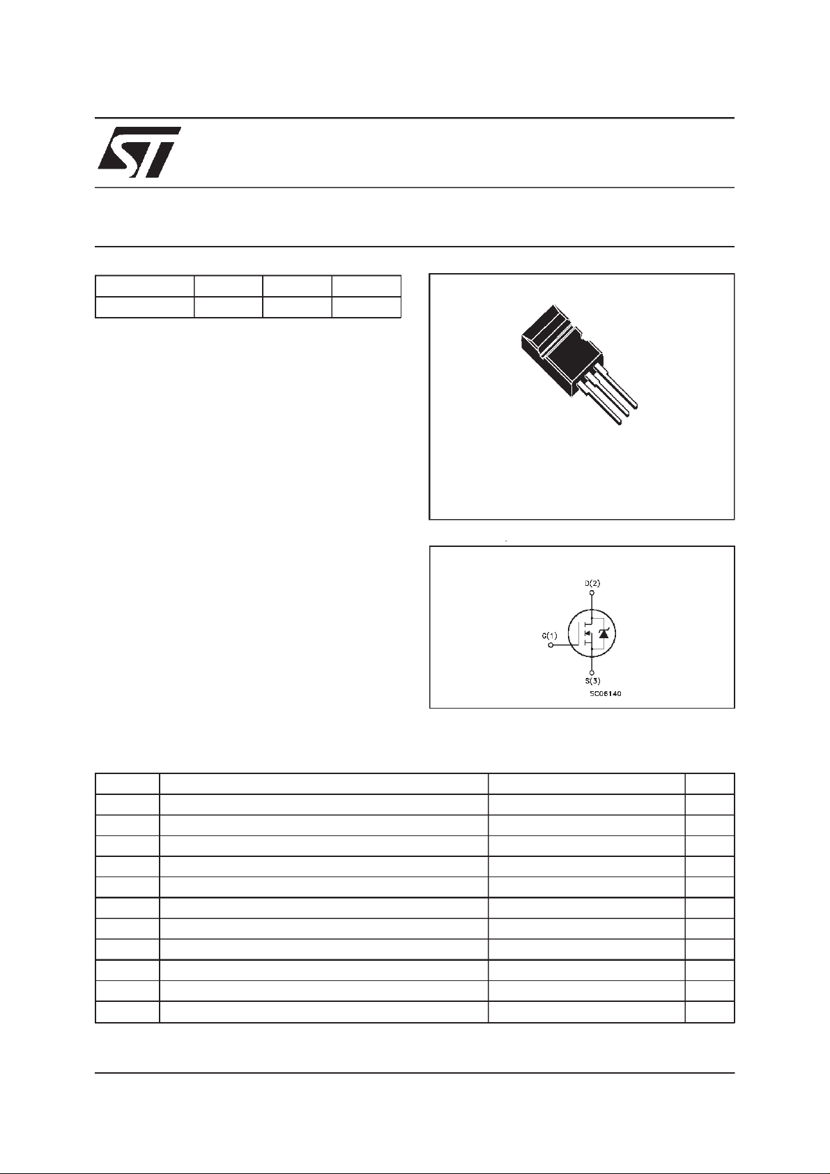
3
2
1
Max220
INTERNAL SCHEMATIC DIAGRAM
ABSOLUTE MAXIMUM RATINGS
Symbol Parameter Value Unit
V
V
V
I
DM
P
dv/ dt(
T
(•) Pulsewidth limited by safe operating area (1)ISD≤16A, di/dt ≤ 200 A/µs, VDD≤ V
September 1999
This is preliminaryinformation on a newproduct now in development or undergoing evaluation. Details are subject to change withoutnotice.
Drain-source Voltage (VGS=0) 500 V
DS
Dra in- gate Voltage (RGS=20kΩ)
DGR
Gate -sourc e Volta ge ± 30 V
GS
I
Drain C urrent (co ntinuous) at Tc=25oC15.6A
D
I
Drain C urrent (co ntinuous) at Tc=100oC9.8A
D
500 V
(•) Drain C urrent (pu lsed) 62 A
Total Dissipation at Tc=25oC160W
tot
Derating Factor 1.28 W/
1) P eak Diode Recovery volt age slope 4.5 V/ns
St orage T e m pe rature -65 t o 150
stg
T
Max. Opera t ing Junct io n T emper at u re 150
j
,Tj≤T
(BR)DSS
JMAX
o
C
o
C
o
C
1/6
Page 2

STU16NB50
THERMAL DATA
R
thj-case
Rthj-a mb
R
thc-sink
T
AVALANCHE CHARACTERISTICS
Symbol Para meter Max Val ue Uni t
I
AR
E
Ther mal Resis t an ce Junc ti on-cas e Max
Ther mal Resis t an ce Junc ti on-ambient Max
Thermal Resistance Case-sink Typ
Maximum Lead Temperat ure F or S old er ing Purpose
l
Avalanche Current , Repetit iv e or No t -Repet it ive
(pulse width limited by T
Single Pulse Avalanche Energy
AS
(starting T
=25oC, ID=IAR,VDD=50V)
j
max)
j
0.78
62.5
0.5
300
15.6 A
850 mJ
o
C/W
oC/W
o
C/W
o
C
ELECTRICAL CHARACTERISTICS (T
=25oC unless otherwisespecified)
case
OFF
Symbol Parameter Test Condit ions Min. Typ. M ax. Unit
V
(BR)DSS
Drain-sourc e
=250µAVGS= 0 @ 100oC
I
D
500 V
Break d own Volt age
I
DSS
I
GSS
Zero Gate Voltage
Drain Current (V
GS
Gat e- b ody Leakage
Current (V
DS
=0)
=0)
V
=MaxRating
DS
= Max Rating Tc=125oC
V
DS
= ± 30 V
V
GS
1
50
± 100 nA
ON(∗)
Symbol Parameter Test Condit ions Min. Typ. M ax. Unit
V
GS(th)
Gate Threshold
V
DS=VGSID
= 250 µA
345V
Voltage
R
DS(on)
Static Drain-source On
VGS=10V ID=7.8 A 0.28 0.33
Resistanc e
I
D(on)
On S t ate Dra in Current VDS>I
D(on)xRDS(on)max
15.6 A
VGS=10V
DYNAMIC
Symbol Parameter Test Condit ions Min. Typ. M ax. Unit
g
(∗)Forward
fs
Tr ansconduc tance
C
C
C
Input Capaci t an c e
iss
Out put Capacitance
oss
Reverse Transfer
rss
Capacitance
VDS>I
D(on)xRDS(on)maxID
=7.8 A 9 S
VDS=25V f=1MHz VGS= 0 2850
400
42
3710
520
55
µA
µ
Ω
pF
pF
pF
A
2/6
Page 3

STU16NB50
ELECTRICAL CHARACTERISTICS
(continued)
SWITCHINGON
Symbol Parameter Test Condit ions Min. Typ. M ax. Unit
t
d(on)
Q
Q
Q
Turn-on Time
t
Rise Time
r
Total Gate Charge
g
Gat e- Source Charge
gs
Gate-Drain Charge
gd
VDD= 250 V ID=7.8A
=4.7 Ω VGS=10V
R
G
VDD= 400 V ID=15.6 A VGS=10V 67
30
15
20
30
42
21
88 nC
SWITCHINGOFF
Symbol Parameter Test Condit ions Min. Typ. M ax. Unit
t
r(Voff)
t
t
Off -voltage Rise Time
Fall Time
f
Cross-ov er Time
c
VDD= 400 V ID= 15. 6 A
=4.7 Ω VGS=10V
R
G
20
15
35
26
21
49
SOURCEDRAINDIODE
Symbol Parameter Test Condit ions Min. Typ. M ax. Unit
I
SD
I
SDM
V
SD
t
Q
I
RRM
(∗) Pulsed: Pulse duration = 300 µs, duty cycle 1.5 %
(•) Pulse width limited by safe operating area
Source-drain Current
(•)
Source-drain Current
15.6
62
(pulsed)
(∗) F orward On Voltage ISD=15.6A VGS=0 1.6 V
Reverse Recov ery
rr
Time
Reverse Recov ery
rr
= 15. 6 A di/dt = 100 A/µs
I
SD
= 100 V Tj=150oC
V
DD
600
6.8
Charge
Reverse Recov ery
22.5
Current
ns
ns
nC
nC
ns
ns
ns
A
A
ns
µ
A
C
3/6
Page 4

STU16NB50
Fig. 1:
UnclampedInductive Load Test Circuit
Fig. 3: Switching Times Test CircuitsFor
ResistiveLoad
Fig. 2:
UnclampedInductive Waveform
Fig. 4: Gate Charge test Circuit
Fig. 5:
Test CircuitFor InductiveLoad Switching
And Diode Recovery Times
4/6
Page 5

Max220 MECHANICAL DATA
STU16NB50
DIM.
MIN. TYP. MAX. MIN. TYP. MAX.
A 4.3 4.6 0.169 0.181
A1 2.2 2.4 0.087 0.094
A2 2.9 3.1 0.114 0.122
b 0.7 0.93 0.027 0.036
b1 1.25 1.4 0.049 0.055
b2 1.2 1.38 0.047 0.054
c 0.45 0.6 0.18 0.023
D 15.9 16.3 0.626 0.641
D1 9 9.35 0.354 0.368
D2 0.8 1.2 0.031 0.047
D3 2.8 3.2 0.110 0.126
e 2.44 2.64 0.096 0.104
E 10.05 10.35 0.396 0.407
L 13.2 13.6 0.520 0.535
L1 3 3.4 0.118 0.133
mm inch
D3 D1
D2
C
A
E
A2
A1
D
b1
b2
L1
L
b
e
P011R
5/6
Page 6

STU16NB50
Information furnished is believed tobe accurateand reliable. However, STMicroelectronics assumes no responsibilityforthe consequences
of use of such information nor for any infringement of patents or other rights of third parties which may result from its use. No license is
granted by implication or otherwise under any patent or patent rights of STMicroelectronics. Specificationmentioned in this publication are
subjecttochange without notice. Thispublication supersedes andreplaces all information previouslysupplied.STMicroelectronics products
are not authorized for use as critical components in lifesupport devices or systemswithout express written approval of STMicroelectronics.
The ST logo is a trademark of STMicroelectronics
1999 STMicroelectronics – Printed in Italy – All Rights Reserved
STMicroelectronics GROUP OF COMPANIES
Australia - Brazil - Canada - China - France - Germany - Italy - Japan- Korea - Malaysia - Malta - Mexico - Morocco - The Netherlands -
6/6
Singapore - Spain - Sweden - Switzerland - Taiwan - Thailand - United Kingdom - U.S.A.
http://www.st.com
.
 Loading...