

Page 1
®
STPR1020CB(-TR)
HIGH EFFICI EN CY FAST RECO VE RY REC T IFIER DIODES
MAIN PRODUCT CHARACTERISTIC S
I
F(AV)
V
RRM
(max) 35 ns
t
rr
2 x 5 A
200 V
FEATURES AND BENEFITS
SUITED FOR SMPS AND DRIVES
SURFACE MOUNT
VERY LOW FORWARD LOSSES
NEGLIGIBLE SWITCHING LOSS ES
HIGH SURGE CURRENT CA PABILITY
SURFACE M OUNT DE V ICE
TAPE AND REEL OPTION : -TR
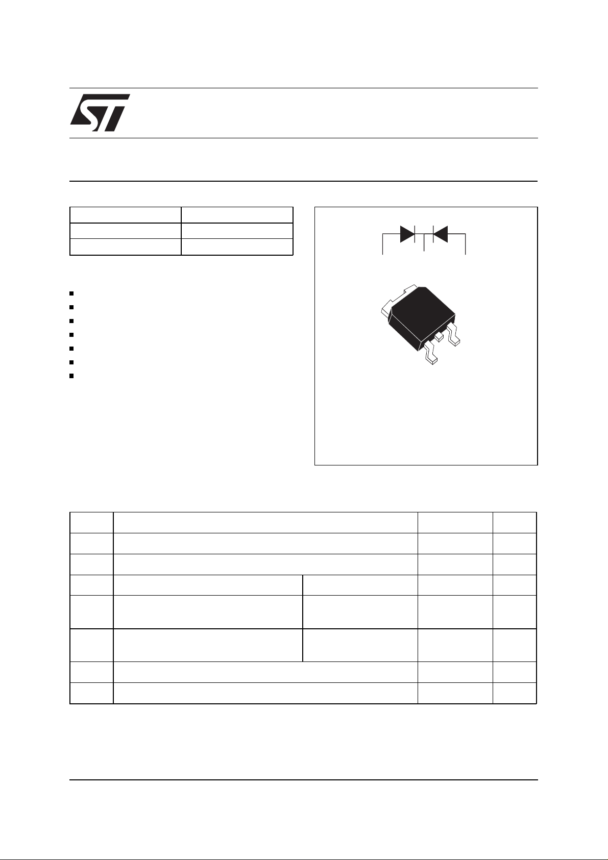
DESCR IPTION
Dual rectifier suited for Switch Mode and high frequency converters.
Packaged in DPAK, this surface mount device is
intended for use in low voltage, high frequency inverters, free wheeling and polarity protection applications.
1
PRELIMINARY DATASHEET
2, 4(TAB)
4
3
2
3
1
DPAK
(Plastic)
ABSOLUTE MAXIMUM RATINGS
Symbol Parameter Value Unit
V
RRM
V
RSM
I
F(RMS)
I
F(AV)
I
FSM
Repetitive Peak Reverse Voltage 200 V
Non Repetitive Surge Reverse V olt age 220 V
RMS Forward Current Per diode 10 A
Average Forward Current
T
= 130°C δ = 0.5
case
Surge Non Repetitive Forward Current
Per diode
Per device
5
10
Per diode 70 A
tp = 10 ms Sinusoidal
Tstg Storage Temperature Range - 40 to + 150
Tj Max. Junction Temperature 150 °C
February 1999 - Ed : 2B
A
°
C
1/3
Page 2

STPR1020CB(-T R)
THERMAL RESISTANCES
Symbol Parameter Value Unit
R
R
th (j-c)
th (c)
Junction to Case Thermal Resistance Per diode 5
Coupling °C/W
When the diodes 1 and 2 are used simultaneously :
∆
Tj(diode 1) = P(diode) x R
(per diode) + P(diode 2) x R
th
Total 2.7
th (c)
°
C/W
STATIC ELECTRICAL CHARACTERISTICS
(per diode)
Symbol Tests Conditions Tests Conditions Min. Typ. Max. Unit
I
* Reverse leakage Current Tj = 25°CV
R
= V
R
RRM
20
Tj = 100°C0.150.5mA
V
** Forward Voltage drop Tj = 25°CI
F
Tj = 100°CI
Pulse test : * tp = 5 ms, duty cycle < 2 %
** tp = 380 µs, duty cycle < 2%
To evaluate the maximum conduction losses use the foll owing equati on :
P = 0.7 x I
F(AV)
+ 0.030 I
F2(RMS)
= 10 A 1.25 V
F
= 5 A 0.8 0.85
F
RECOVERY CH ARACTE RIST ICS
Symbol Test Conditions Min. Typ. Max. Unit
t
rr
t
fr
V
FP
Tj = 25°C IF = 1A
V
= 30V
F
Tj = 25°C IF = 1A
V
= 1.1 x V
FR
F
Tj = 25°C IF = 1A tr = 10 ns 5 V
/dt = -50 Α/ms 35 ns
dI
F
tr = 10 ns 20 ns
µ
A
2/3
Page 3

PACKAGE ME CHANICAL D AT A
DPAK
STPR1020CB( -TR)
DIMENSIONS
REF.
A 2.20 2.40 0.086 0.094
A1 0.90 1.10 0.035 0.043
A2 0.03 0.23 0.001 0.009
B 0.64 0.90 0.025 0.035
B2 5.20 5.40 0.204 0.212
C 0.45 0.60 0.017 0.023
C2 0.48 0.60 0.018 0.023
D 6.00 6.20 0.236 0.244
E 6.40 6.60 0.251 0.259
G 4. 40 4.60 0.173 0.181
H 9.35 10.10 0.368 0.397
L2 0.80 0.031
L4 0.60 1.00 0.023 0.039
V2 0° 8° 0° 8°
Millimeters Inches
Min. Typ. Max Min. Typ. Max.
FOOT PRINT
Information furnished is believed to be accurate and reliable. However, STMicroelectronics assumes no responsibility for the consequences of
use of such information nor for any infringement of patents or other rights of third parties which may result from its use. No license is granted by
implication or oth erwise under any patent or patent rights of STMi croelectronics . Specifications mentioned i n this publication are subjec t to
change without notice. This publication supersedes and replaces all information previously supplied.
STMicroelectr oni cs products are not authorized for use as critical components in l i fe s upport devices or systems without express written approval of STMicroelectronics.
Australia - Brazil - Canada - China - France - Germany - Italy - Japan - Korea - Malaysia - Malta - Mexico - Morocco -
The Netherlands - Singapore - Spain - Sweden - Switzerland - Taiwan - Thailand - United Kingdom - U.S.A.
in millimeters
6.7
6.7
6.7
3
1.61.6
2.32.3
The ST logo is a registered trademark o f STMicroelectron ics
© 1999 STMicroelectronics - Printed in Italy - All rights reserved.
STMicroelectronics GROUP OF COMPANIES
http://www.st.com
3/3
 Loading...