

Page 1
STP9NK65Z
STP9NK65ZFP
N-CHANNEL 650V - 1Ω - 7A TO-220/TO-220FP
Zener-Protected SuperMESH™Power MOSFET
TARGET DATA
TYPE V
STP9NK65Z
STP9NK65ZFP
■ TYPICAL R
■ EXTREMELY HIGH dv/dtCAPABILITY
■ IMPROVED ESD CAPABILITY
■ 100% AVALANCHE RATED
■ GATE CHARGE MINIMIZED
■ VERY LOW INTRINSIC CAPACITANCES
■ VERY GOOD MANUFACTURING
650 V
650 V
(on) = 1.0 Ω
DS
DSS
R
DS(on)
< 1.2 Ω
< 1.2 Ω7A7A
I
D
Pw
110 W
30 W
REPEATIBILITY
DESCRIPTION
The SuperM ESH™ s eries is obtained through an
extreme optimi za tio n of ST’s well established stripbased PowerMESH™ layout. In addition to pushing
on-resistance significantly down, spec ial care is taken to ensure a very good dv/dt capability fo r the
most demanding applications. Such series com plements ST full range of high voltage MOSF ETs including revolutionary MDmesh™ products.
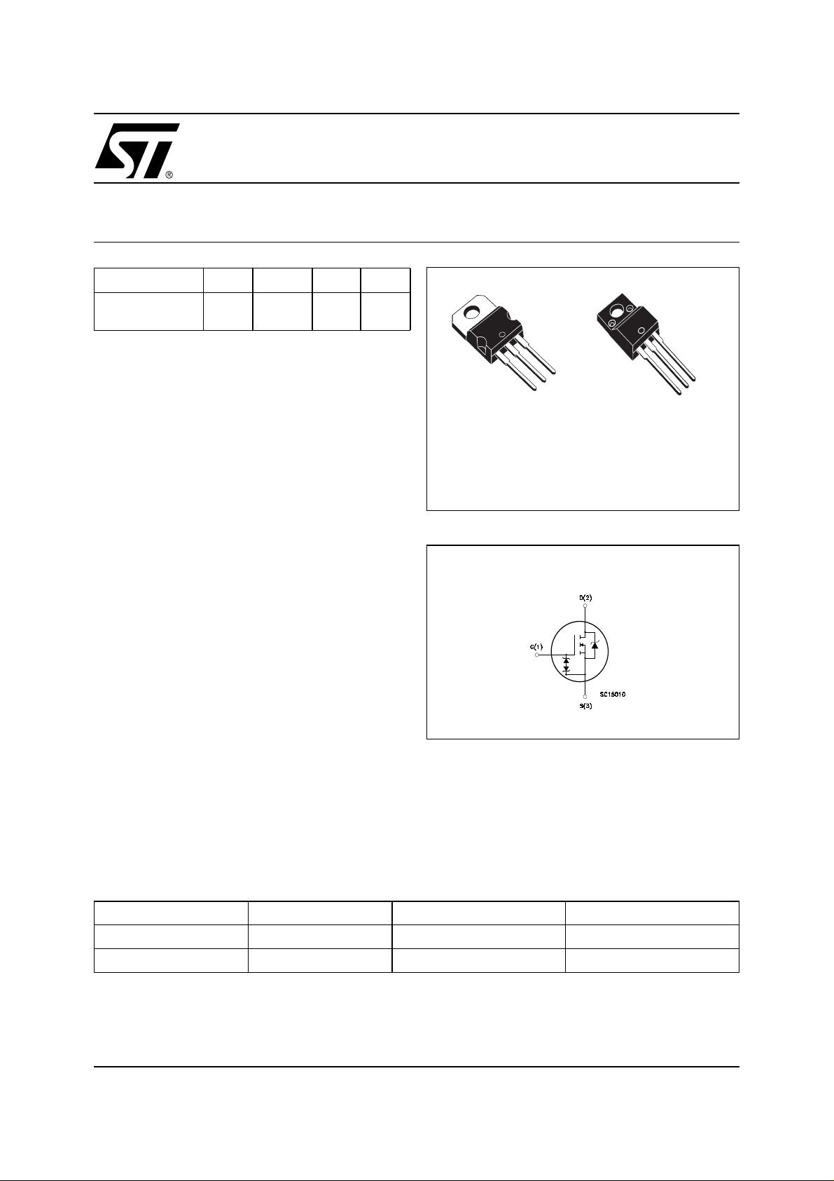
3
2
TO-220
1
TO-220FP
1
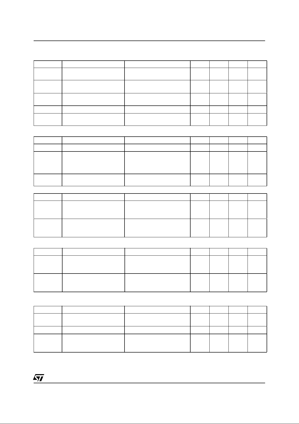
INTERNAL SCHEMATIC DIAGRAM
3
2
APPLICATIONS
■ HIGH CURRENT, HIGH SPEED SWITCHING
■ IDEAL FOR OFF-LINE POWER SUPPLIES,
ADAPTORS AND PFC
ORDERING INFORMATION
SALES TYPE MARKING PACKAGE PACKAGING
STP9NK65Z P9NK65Z TO-220 TUBE
STP9NK65ZFP P9NK65ZFP TO-220FP TUBE
July 2003
1/7
Page 2

STP9NK65 - ST P9NK 65ZFP
ABSOLUTE MAXIMUM RATINGS
Symbol Parameter Value Unit
STP9NK65Z STP9NK65ZFP
V
DS
V
DGR
V
GS
I
D
I
D
IDM()
P
TOT
V
ESD(G-S)
dv/dt (1) Peak Diode Recovery voltage slope TBD V/ns
V
ISO
T
j
T
stg
() Pulse width limited by safe operating area
(1) I
≤TBD, di/dt ≤TBD, VDD≤ V
SD
(*) Limited only by maximum temperature allowed
Drain-source Voltage (VGS=0)
Drain-gate Voltage (RGS=20kΩ)
650 V
650 V
Gate- source Voltage ± 30 V
Drain Current (continuous) at TC= 25°C
Drain Current (continuous) at TC= 100°C
7 7 (*) A
4.4 4.4 (*) A
Drain Current (pulsed) 28 28 (*) A
Total Dissipation at TC= 25°C
110 30 W
Derating Factor 0.88 0.24 W/°C
Gate source ESD(HBM-C=100pF, R=1.5KΩ) 3500 KV
Insulation Withstand Voltage (DC) - 2500 V
Operating Junction Temperature
Storage Temperature
(BR)DSS,Tj≤TJMAX.
-55 to 150
-55 to 150
°C
°C
THERMAL DATA
TO-220 TO-220FP
Rthj-case Thermal Resistance Junction-case Max 1.14 4.2 °C/W
Rthj-amb Thermal Resistance Junction-ambient Max 62.5 °C/W
T
l
Maximum Lead Temperature For Soldering Purpose
300 °C
AVALANCHE CHARACTERISTICS
Symbol Parameter Max Value Unit
I
AR
Avalanche Current, Repetitive or Not-Repetitive
(pulse width limited by T
E
AS
Single Pulse Avalanche Energy
(starting T
max)
j
= 25 °C, ID=IAR,VDD=50V)
j
7A
TBD mJ
GATE-SOURCE ZENER DIODE
Symbol Parameter Test Conditions Min. Typ. Max. Unit
BV
GSO
Gate-Source Breakdown
Igs=± 1mA (Open Drain) 30 V
Voltage
PROTECTION FEATURES OF GATE-TO-SOURCE ZENER DIOD ES
The built-in bac k-to-back Zener diodes have specif ically been designed to enhance not only the device’s
ESD capability, but also to make them s a fely absorb possible voltage transients that may occasionally be
applied from gate tosouce. In this respect the Zener voltage is appropriateto achieve an efficient and costeffective intervention to protect the device’s integrity. These integrated Zener diodes thus avoid the usage
of external components.
2/7
Page 3
STP9NK65 - ST P9NK 65ZFP
ELECTRICAL CHARACTERISTICS (TCASE =25°C UNLESS OTHERWISE SPECIFIED)
ON/OFF
Symbol Parameter Test Conditions Min. Typ. Max. Unit
V
(BR)DSS
Drain-source
Breakdown Voltage
I
DSS
I
GSS
V
GS(th)
R
DS(on)
Zero Gate Voltage
Drain Current (V
GS
=0)
Gate-body Leakage
Current (V
DS
=0)
Gate Threshold Voltage
Static Drain-source On
Resistance
DYNAMIC
Symbol Parameter Test Conditions Min. Typ. Max. Unit
(1) Forward Transconductance VDS=8V,ID= 3 A TBD S
g
fs
Input Capacitance
Output Capacitance
Reverse Transfer
Capacitance
(3) Equivalent Output
C
oss eq.
C
iss
C
oss
C
rss
Capacitance
SWITCHING ON
Symbol Parameter Test Conditions Min. Typ. Max. Unit
t
d(on)
Q
Q
Q
t
r
g
gs
gd
Turn-on Delay Time
Rise Time
Total Gate Charge
Gate-Source Charge
Gate-Drain Charge
ID=1mA,VGS= 0 650 V
V
= Max Rating
DS
VDS= Max Rating, TC= 125 °C
V
= ± 20V ±10 µA
GS
V
DS=VGS,ID
= 100µA
3 3.75 4.5 V
1
50
VGS=10V,ID= 3 A 1.0 1.2 Ω
=25V,f=1MHz,VGS= 0 TBD
V
DS
TBD
TBD
VGS=0V,VDS= 0V to 480V TBD pF
VDD=325V,ID=3A
RG= 4.7Ω VGS=10V
TBD
TBD
(Resistive Load see, Figure 3)
=520V,ID=6A,
V
V
DD
GS
=10V
TBD
TBD
TBD
µA
µA
pF
pF
pF
ns
ns
nC
nC
nC
SWITCHING OFF
Symbol Parameter Test Conditions Min. Typ. Max. Unit
t
d(off)
Turn-off Delay Time
t
f
Fall Time
VDD= 325 V, ID=3A
R
=4.7ΩVGS=10V
G
TBD
TBD
(Resistive Load see, Figure 3)
t
r(Voff)
t
t
Off-voltage Rise Time
f
c
Fall Time
Cross-over Time
= 520 V, ID=6A,
V
DD
RG=4.7Ω, VGS= 10V
(Inductive Load see, Figure 5)
TBD
TBD
TBD
SOURCE DRAIN DIODE
Symbol Parameter Test Conditions Min. Typ. Max. Unit
I
SD
I
SDM
VSD(1)
t
rr
Q
rr
I
RRM
Note: 1. Pulsed: Pulse duration = 300 µs, duty cycle 1.5 %.
2. Pulse width limited by safe operating area.
3. C
Source-drain Current
(2)
Source-drain Current (pulsed)
Forward On Voltage
Reverse Recovery Time
Reverse Recovery Charge
Reverse Recovery Current
is defined as a constant equivalent capacitance giving the same charging time as C
oss eq.
.
V
DSS
ISD= 7 A, VGS=0
I
SD
VDD=35V,Tj= 150°C
(see test circuit, Figure 5)
= 6 A, di/dt = 100A/µs
TBD
TBD
TBD
when VDSincreases from 0 to 80%
oss
7
28
1.6 V
ns
ns
ns
ns
ns
A
A
ns
µC
A
3/7
Page 4

STP9NK65 - ST P9NK 65ZFP
Fig. 2: Unclamped Inductive WaveformFig. 1: Unclamped Inductive Load Test Circuit
Fig. 3: Switching Times Test Circuit For
Resistive Load
Fig. 5: Test Circuit For Inductive Load Switching
And Di ode Recovery Times
Fig. 4: Gate Charge test Circuit
4/7
Page 5

E
TO-220 MECHANICAL DATA
P011C
STP9NK65 - ST P9NK 65ZFP
DIM.
A 4.40 4.60 0.173 0.181
C 1.23 1.32 0.048 0.051
D 2.40 2.72 0.094 0.107
D1 1.27 0.050
E 0.49 0.70 0.019 0.027
F 0.61 0.88 0.024 0.034
F1 1.14 1.70 0.044 0.067
F2 1.14 1.70 0.044 0.067
G 4.95 5.15 0.194 0.203
G1 2.4 2.7 0.094 0.106
H2 10.0 10.40 0.393 0.409
L2 16.4 0.645
L4 13.0 14.0 0.511 0.551
L5 2.65 2.95 0.104 0.116
L6 15.25 15.75 0.600 0.620
L7 6.2 6.6 0.244 0.260
L9 3.5 3.93 0.137 0.154
DIA. 3.75 3.85 0.147 0.151
MIN. TYP. MAX. MIN. TYP. MAX.
mm inch
A
C
D
L5
Dia.
L7
D1
L6
L2
L9
F1
G1
F
H2
G
F2
L4
5/7
Page 6

STP9NK65 - ST P9NK 65ZFP
TO-220FP MECHANICAL DATA
DIM.
A 4.4 4.6 0.173 0.181
B 2.5 2.7 0.098 0.106
D 2.5 2.75 0.098 0.108
E 0.45 0.7 0.017 0.027
F 0.75 1 0.030 0.039
F1 1.15 1.5 0.045 0.067
F2 1.15 1.5 0.045 0.067
G 4.95 5.2 0.195 0.204
G1 2.4 2.7 0.094 0.106
H 10 10.4 0.393 0.409
L2 16 0.630
L3 28.6 30.6 1.126 1.204
L4 9.8 10.6 .0385 0.417
L5 2.9 3.6 0.114 0.141
L6 15.9 16.4 0.626 0.645
L7 9 9.3 0.354 0.366
Ø 3 3.2 0.118 0.126
MIN. TYP MAX. MIN. TYP. MAX.
mm. inch
E
A
D
B
L3
L6
L7
¯
F1
F
G1
H
G
F2
123
L2
L5
L4
6/7
Page 7

STP9NK65 - ST P9NK 65ZFP
Information furnished is believed to be accurate and reliable. However, STMicroelectronics assumes no responsibility for the
consequences of use o f suc h inf ormat ion n or f or an y infr ingeme nt of paten ts or oth er ri gh ts of third part ies whic h may resul t f rom
its use. No license is granted by implication or otherwise under any patent or patent rights of STMicroelectronics. Specifications
mentioned in this publication are subject to change without notice. This publication supersedes and replaces all information
previously supplied. STMicroelectronics products are not authorized for use as critical components in life support devices or
systems without express written approval of STMicroelectronics.
© The ST logo is a registered trademark of STMicroelectronics
© 2003 STMicroelectronics - Printed in Italy - All Rights Reserved
STMicroelectronics GROUP OF COMPANIES
Australia - Brazil - Canada - China - Finland - France - Germany - Hong Kong - India - Israel - Italy - Japan - Malaysia - Malta - Morocco
Singapore - Spain - Sweden - Switzerland - United Kingdom - United States.
© http://www.st.com
7/7
 Loading...