

Page 1

STP9NC60
N - CHANNEL 600V- 0.6Ω - 9A TO-220/TO-220FP
TYPE V
ST P9 NC60
ST P9 NC60FP
ν TYPICALR
ν EXTREMELYHIGHdv/dtCAPABILITY
ν 100%AVALANCHETESTED
ν NEWHIGH VOLTAGE BENCHMARK
ν GATECHARGE MINIMIZED
DS(on)
DSS
600 V
600 V
= 0.6 Ω
DESCRIPTION
The PowerMESHII is the evolution of the first
generation of MESH OVERLAY. The layout
refinements introduced greatly improve the
Ron*area figure of merit while keeping the device
at the leading edge for what concerns switching
speed, gate charge and ruggedness.
APPLICATIONS
ν HIGHCURRENT, HIGH SPEEDSWITCHING
ν SWITHMODE POWERSUPPLIES (SMPS)
ν DC-ACCONVERTERSFOR WELDING
EQUIPMENTAND UNINTERRUPTIBLE
POWERSUPPLIESAND MOTORDRIVER
R
DS(on)
<0.75Ω
<0.75Ω
I
D
9.0 A
5.2 A
STP9NC60FP
PowerMESH ΙΙ MOSFET
3
2
1
TO-220 TO-220FP
INTERNAL SCHEMATIC DIAGRAM
3
2
1
ABSOLUTE MAXIMUM RATINGS
Symbol Parameter Value Uni t
ST P9NC6 0 ST P9 NC60FP
V
V
V
I
DM
P
dv/dt(
V
T
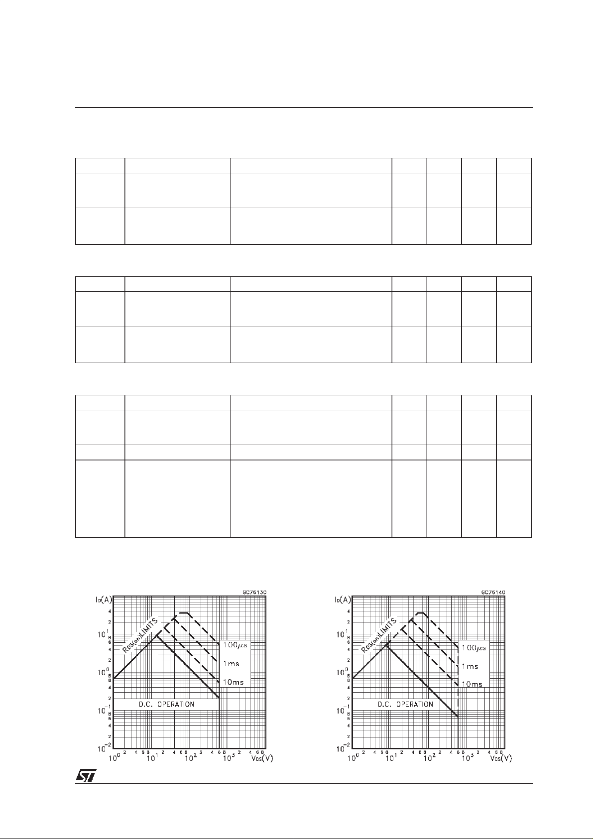
(•) Pulse width limited by safe operating area (1)ISD≤ 9A, di/dt ≤ 200 A/µs, VDD≤ V
February 2000
Drain-source Vol t age (VGS= 0) 600 V
DS
Drain- gate V oltage (RGS=20kΩ)
DGR
Gate-s ource Voltage ± 30 V
GS
I
Drain C urr ent (c ont inuous) at Tc=25oC9.05.2A
D
Drain C urr ent (c ont inuous) at Tc= 100oC5.73.3A
I
D
600 V
(•) Drain Curr ent (p ulsed) 36 36 A
Tot al Dissipation at Tc=25oC 125 40 W
tot
Derating Fact or 1.0 0.32 W/
1) Peak Di ode Rec ov ery v olt a ge slope 4.5 4.5 V/ ns
Insulation Withstand Voltage (DC) 2000 V
ISO
St orage Te mper ature -65 to 150
stg
T
Max. Oper ating Ju nction Tem perat ure 150
j
(BR)DSS
,Tj≤T
JMAX
o
C
o
C
o
C
1/9
Page 2
STP9NC60/FP
THERMAL DATA
TO-220 TO - 220FP
R
thj-cas e
R
thj-amb
R
thc-sin k
T
AVALANCHE CHARACTERISTICS
Symb ol Parameter Max Val ue Uni t
I
AR
E
Therma l Resist ance Junction- case Max 1.0 3. 12
Therma l Resist ance Junction- ambient Max
Therma l Resist ance Case-sink Typ
Maxim um Lea d Te m pe rat ur e For Soldering Purpose
l
Avalanc h e Current, Repetit ive or Not-Repetitive
(pulse width limited by T
Single Pulse Av alanche E nergy
AS
(starting T
=25oC, ID=IAR,VDD=50V)
j
max, δ <1%)
j
62.5
0.5
300
9A
850 mJ
o
C/W
o
C/W
o
C/W
o
C
ELECTRICAL CHARACTERISTICS (T
=25oC unlessotherwisespecified)
case
OFF
Symb ol Param et er Test C o n diti o n s Mi n . Typ . Max. Unit
V
(BR) DSS
Drain-s ource
= 250 µAVGS=0
I
D
600 V
Break down Voltage
I
DSS
I
GSS
Zero G ate Voltage
Drain Current (V
GS
Gate-body Leak a ge
Current (V
DS
=0)
=0)
V
=MaxRating
DS
= Max Rating Tc= 125oC
V
DS
= ± 30 V
V
GS
1
50
± 100 nA
ON (∗)
Symb ol Param et er Test C o n diti o n s Mi n . Typ . Max. Unit
V
GS(th)
R
DS(on)
Gate Thre shold Voltage
Static Drain- s ource O n
V
DS=VGSID
=250µA
VGS= 10V ID=4A 0.6 0.75 Ω
234V
Resistance
I
D(on)
On State Drain Current VDS>I
D(on)xRDS(on)max
9.0 A
VGS=10V
DYNAMIC
Symb ol Param et er Test C o n diti o n s Mi n . Typ . Max. Unit
g
(∗)Forward
fs
Transconductance
Input Capacitance
iss
Output Capacitance
Reverse Transfer
rss
C
C
oss
C
Capacit ance
VDS>I
D(on)xRDS(on)maxID
=4A 10 S
VDS=25V f=1MHz VGS= 0 1400
196
31
µA
µA
pF
pF
pF
2/9
Page 3
STP9NC60/FP
ELECTRICAL CHARACTERISTICS (continued)
SWITCHING ON
Symb ol Param et er Test C o n diti o n s Mi n . Typ . Max. Unit
t
d(on)
t
Turn-on Delay T ime
Rise Tim e
r
VDD=300V ID=4.5A
=4.7 Ω VGS=10V
R
G
(Resis t i ve Load, s ee fi g. 3)
Q
Q
Q
Total Gate Charge
g
Gate-Source Charge
gs
Gate-Drain Charge
gd
VDD=480V ID=9.0A VGS=10V 44
SWITCHING OFF
Symb ol Param et er Test C o n diti o n s Mi n . Typ . Max. Unit
t
d(off)
t
Turn-off Delay Time
Fall T ime
f
VDD=300V ID=4.5A
=4.7 Ω VGS=10V
R
G
(Resis t i ve Load, s ee fi g. 3)
t
r(Voff)
t
t
Off -voltage Rise Time
Fall T ime
f
Cross -over Time
c
VDD=480V ID=9.0A
=4.7 Ω VGS=10V
R
G
(Inductive Load, see f i g. 5 )
SOURCEDRAIN DIODE
28
15
62 nC
10.5
19.5
53
30
15
12
24
ns
ns
nC
nC
ns
ns
ns
ns
ns
Symb ol Param et er Test C o n diti o n s Mi n . Typ . Max. Unit
I
SDM
I
SD
Source-drain Current
(•)
Source-drain Current
9.0
36
(pulsed)
(∗)ForwardOnVoltage ISD=9A VGS=0 1.6 V
V
SD
t
Q
Revers e R ecover y
rr
Time
Revers e R ecover y
rr
=9A di/dt=100A/µs
I
SD
=100V Tj= 150oC
V
DD
(see test circuit, fig. 5)
610
5.4
Charge
I
RRM
Revers e R ecover y
17
Current
(∗) Pulsed: Pulse duration = 300µs, dutycycle 1.5 %
(•) Pulse width limited by safe operatingarea
Safe OperatingArea for TO-220 Safe OperatingAreafor TO-220FP
A
A
ns
µC
A
3/9
Page 4

STP9NC60/FP
ThermalImpedancefor TO-220
OutputCharacteristics
ThermalImpedance forTO-220FP
TransferCharacteristics
Transconductance
4/9
StaticDrain-sourceOn Resistance
Page 5

STP9NC60/FP
Gate Chargevs Gate-sourceVoltage
NormalizedGate ThresholdVoltagevs
Temperature
CapacitanceVariations
Normalized On Resistance vs Temperature
Source-drainDiode Forward Characteristics
5/9
Page 6

STP9NC60/FP
Fig. 1: UnclampedInductive Load Test Circuit
Fig. 3: SwitchingTimes Test CircuitsFor
ResistiveLoad
Fig. 2: UnclampedInductive Waveform
Fig. 4: GateChargetest Circuit
Fig. 5: Test CircuitFor InductiveLoad Switching
And Diode Recovery Times
6/9
Page 7

TO-220 MECHANICAL DATA
STP9NC60/FP
DIM.
MIN. TYP. MAX. MIN. TYP. MAX.
A 4.40 4.60 0.173 0.181
C 1.23 1.32 0.048 0.0 51
D 2.40 2.72 0.094 0.107
D1 1.27 0.050
E 0.49 0.70 0.019 0.0 27
F 0.61 0.88 0.024 0.034
F1 1.14 1.70 0.044 0.067
F2 1.14 1.70 0.044 0.067
G 4.95 5.15 0.194 0.203
G1 2.4 2.7 0.094 0.106
H2 10.0 1 0.40 0.393 0.4 09
L2 16.4 0.645
L4 13. 0 14.0 0.511 0.551
L5 2.65 2.95 0.104 0.116
L6 15.25 15.75 0.600 0.6 20
L7 6.2 6.6 0.244 0.260
L9 3.5 3.93 0.137 0.154
DIA. 3.75 3.85 0.147 0.1 51
mm inch
E
A
L4
D
F2
F1
G1
H2
G
F
P011C
C
D1
L2
Dia.
L5
L7
L6
L9
7/9
Page 8

STP9NC60/FP
TO-220FP MECHANICAL DATA
DIM.
MIN. TYP. MAX. MIN. TYP. MAX.
A 4 .4 4.6 0. 173 0.181
B 2.5 2.7 0. 098 0.106
D 2.5 2.75 0.098 0.108
E 0.45 0.7 0.017 0.027
F 0.75 1 0.030 0.039
F1 1. 15 1.7 0. 045 0.067
F2 1. 15 1.7 0. 045 0.067
G 4.95 5.2 0.195 0.204
G1 2.4 2.7 0.094 0.106
H 10 10.4 0. 393 0.409
L2 16 0.630
L3 28. 6 30.6 1.126 1.204
L4 9.8 10.6 0.385 0.4 17
L6 15. 9 16.4 0.626 0.645
L7 9 9.3 0.354 0.366
Ø 3 3.2 0.118 0.126
mm inch
E
A
D
B
L3
L6
L7
¯
F1
F
G1
H
G
F2
123
L2
L4
8/9
Page 9

STP9NC60/FP
Information furnished is believed tobe accurateand reliable.However,STMicroelectronics assumes no responsibilityfor the consequences
of use of such information nor for any infringement of patents or other rights of third parties which may result from its use. No license is
granted by implication or otherwise under any patent or patentrightsof STMicroelectronics. Specification mentioned in this publication are
subjectto change withoutnotice.This publication supersedes and replaces allinformation previously supplied.STMicroelectronicsproducts
are not authorized for use as critical components in life supportdevices or systems without express written approval of STMicroelectronics.
The ST logo is a trademark of STMicroelectronics
1999 STMicroelectronics – Printed in Italy – All Rights Reserved
STMicroelectronics GROUP OF COMPANIES
Australia - Brazil - China - Finland - France - Germany - Hong Kong - India - Italy - Japan - Malaysia - Malta - Morocco -
Singapore - Spain - Sweden - Switzerland - United Kingdom - U.S.A.
http://www.st.com
.
9/9
 Loading...