

Page 1

STP9NB60
N - CHANNEL 600V - 0.7Ω - 9A TO-220/TO220FP
TYPE V
STP9NB60
STP9NB60 FP
■ TYPICALR
■ EXTREMELYHIGH dv/dt CAPABILITY
■ 100%AVALANCHETESTED
■ VERYLOW INTRINSIC CAPACITANCES
■ GATECHARGE MINIMIZED
DS(on)
DSS
600 V
600 V
= 0.7
DESCRIPTION
Using the latest high voltageMESHOVERLAY
process, STMicroelectronics has designed an
advanced family of power MOSFETs with
outstanding performances. The new patent
pending strip layout coupled with the Company’s
proprietary edge termination structure, gives the
lowest RDS(on) per area, exceptional avalanche
and dv/dt capabilities and unrivalled gate charge
and switching characteristics.
Ω
R
DS(on)
<0.8Ω
<0.8
Ω
I
D
9.0 A
9.0 A
STP9NB60FP
PowerMESH MOSFET
3
2
1
TO-220 TO-220FP
INTERNAL SCHEMATIC DIAGRAM
3
2
1
APPLICATIONS
■ HIGHCURRENT, HIGHSPEED SWITCHING
■ SWITCHMODE POWER SUPPLIES(SMPS)
■ DC-AC CONVERTERS FOR WELDING
EQUIPMENTAND UNINTERRUPTIBLE
POWERSUPPLIESAND MOTORDRIVE
ABSOLUTE MAXIMUM RATINGS
Symbol Parameter Value Unit
ST P9 NB60 STP 9NB 60FP
V
V
V
I
DM
P
dv/ dt(
V
T
(•) Pulse width limited by safe operating area (1)ISD≤ 9A, di/dt ≤ 200 A/µs,VDD≤ V
Limited only by maximum temperatureallowed
(*)
January 2000
Drain - source Vo lt age ( VGS=0) 600 V
DS
Drain - gate V olt a ge (RGS=20kΩ)
DGR
Gate-source Voltage
GS
Drain Curre nt (continuous ) at Tc=25oC9.09.0(*)A
I
D
Drain Curre nt (continuous ) at Tc=100oC5.75.7(*)A
I
D
600 V
30 V
±
(•) Drain Curre nt (puls ed) 36 36 A
Total Dissipation at Tc=25oC 125 40 W
tot
Derating F act or 1.0 0.32 W/
) Peak Diode Rec o v e ry voltag e slope 4.5 4.5 V/ns
1
Insulation Withstand Voltage (DC) 2000 V
ISO
Storage Temperature -65 to 150
stg
Max. Operating Junction Temp er ature 150
T
j
,Tj≤T
(BR)DSS
JMAX
o
C
o
C
o
C
1/9
Page 2
STP9NB60/FP
THERMAL DATA
TO-220 TO-220FP
R
thj-case
R
thj-amb
R
thc-sink
T
AVALANCHE CHARACTERISTICS
Symbol Para meter Max Val ue Uni t
I
AR
E
Ther mal Resist ance Junction- c as e Max 1.0 3.12
Ther mal Resist ance Junction- am b ien t Max
Thermal Resistance Case-sink Typ
Maximum Lead Temperat ure F o r Soldering Purp os e
l
Avalanche Current, Repetitive or Not- Re petitive
(pulse width limited by T
Single Pulse Avalanche En ergy
AS
(starting T
=25oC, ID=IAR,VDD=50V)
j
max, δ <1%)
j
62.5
0.5
300
9A
850 mJ
o
C/W
o
C/W
o
C/W
o
C
ELECTRICAL CHARACTERISTICS
=25oC unless otherwisespecified)
(T
case
OFF
Symbol Parameter Test Conditions Min. Typ. M ax. Unit
V
(BR)DSS
Drain-sourc e
=250µAVGS=0
I
D
600 V
Break d own Vo lt age
I
DSS
I
GSS
Zero Gate Voltage
Drain Curr ent (V
GS
Gat e- b ody Leaka ge
Current ( V
DS
=0)
=0)
V
=MaxRating
DS
= Max Rating Tc=125oC
V
DS
=± 30 V
V
GS
1
50
100 nA
±
ON(∗)
Symbol Parameter Test Conditions Min. Typ. M ax. Unit
V
GS(th)
Gate Threshold
V
DS=VGSID
= 250µA
345V
Voltage
R
DS(on)
Static Drain-source On
VGS=10V ID=3A 0.7 0.8 Ω
Resistanc e
I
D(on)
On S t ate Drain Current VDS>I
D(on)xRDS(on)max
9.0 A
VGS=10V
DYNAMIC
Symbol Parameter Test Conditions Min. Typ. M ax. Unit
g
(∗)Forward
fs
Tr ansconductanc e
C
C
C
Input Capacitanc e
iss
Out put Capacit ance
oss
Reverse Transfer
rss
Capacitance
VDS>I
D(on)xRDS(on)maxID
=4.5A 3.0 6.5 S
VDS=25V f=1MHz VGS= 0 1480
210
25
1924
273
33
µ
µA
pF
pF
pF
A
2/9
Page 3

STP9NB60/FP
ELECTRICAL CHARACTERISTICS
(continued)
SWITCHINGON
Symbol Parameter Test Conditions Min. Typ. M ax. Unit
t
d(on)
Turn-on Time
r
Rise Time
t
VDD= 300 V ID=4.5A
R
=4.7
G
Ω
VGS=10V
25
11
35
15
(see test circuit, figure 3)
Q
Q
Q
Total Gate Charge
g
Gat e- Source Charge
gs
Gate-Drain Charge
gd
VDD= 480 V ID=9.0AVGS=10V 40
10.5
17.5
56 nC
SWITCHINGOFF
Symbol Parameter Test Conditions Min. Typ. M ax. Unit
t
r(Voff)
t
t
Off -voltage Rise Time
Fall Time
f
Cross-ov er Tim e
c
VDD= 480 V ID=9.0A
=4.7 ΩVGS=10V
R
G
(see test circuit, figure 5)
12
10
21
17
14
29
SOURCEDRAINDIODE
Symbol Parameter Test Conditions Min. Typ. M ax. Unit
I
SD
I
SDM
V
SD
t
Q
I
RRM
(∗) Pulsed: Pulse duration = 300 µs, duty cycle 1.5 %
(•) Pulse width limited by safe operatingarea
Source-drain Current
(•)
Source-drain Current
9.0
36
(pulsed)
(∗) Forward On Voltage ISD=9.0A VGS=0 1.6 V
Reverse R ec o very
rr
Time
Reverse R ec o very
rr
=9.0A di/dt=100A/µs
I
SD
= 100 V Tj=150oC
V
DD
(see test circuit, figure 5)
600
5.4
Charge
Reverse R ec o very
18
Current
ns
ns
nC
nC
ns
ns
ns
A
A
ns
µ
A
C
SafeOperating Area for TO-220 SafeOperating Area for TO-220FP
3/9
Page 4
STP9NB60/FP
ThermalImpedancefor TO-220
OutputCharacteristics
ThermalImpedanceforTO-220FP
TransferCharacteristics
Transconductance
4/9
Static Drain-sourceOn Resistance
Page 5
STP9NB60/FP
Gate Charge vs Gate-sourceVoltage
Normalized Gate ThresholdVoltage vs
Temperature
CapacitanceVariations
Normalized On Resistance vsTemperature
Source-drainDiode Forward Characteristics
5/9
Page 6

STP9NB60/FP
Fig. 1:
UnclampedInductive Load Test Circuit
Fig. 3: Switching Times Test Circuits For
ResistiveLoad
Fig. 2:
UnclampedInductive Waveform
Fig. 4: Gate Charge test Circuit
Fig. 5:
Test CircuitFor InductiveLoad Switching
And Diode Recovery Times
6/9
Page 7
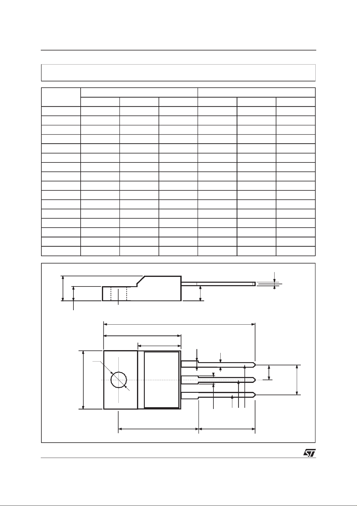
TO-220 MECHANICAL DATA
STP9NB60/FP
DIM.
MIN. TYP. MAX. MIN. TYP. MAX.
A 4.40 4.60 0.173 0.181
C 1.23 1.32 0.048 0.051
D 2.40 2.72 0.094 0.107
D1 1.27 0.050
E 0.49 0.70 0.019 0.027
F 0.61 0.88 0.024 0.034
F1 1.14 1.70 0.044 0.067
F2 1.14 1.70 0.044 0.067
G 4.95 5.15 0.194 0.203
G1 2.4 2.7 0.094 0.106
H2 10.0 10.40 0.393 0.409
L2 16.4 0.645
L4 13.0 14.0 0.511 0.551
L5 2.65 2.95 0.104 0.116
L6 15.25 15.75 0.600 0.620
L7 6.2 6.6 0.244 0.260
L9 3.5 3.93 0.137 0.154
DIA. 3.75 3.85 0.147 0.151
mm inch
E
A
L4
D
F2
F1
G1
H2
G
F
P011C
C
D1
L2
Dia.
L5
L7
L6
L9
7/9
Page 8
STP9NB60/FP
TO-220FP MECHANICAL DATA
DIM.
MIN. TYP. MAX. MIN. TYP. MAX.
A 4.4 4.6 0.173 0.181
B 2.5 2.7 0.098 0.106
D 2.5 2.75 0.098 0.108
E 0.45 0.7 0.017 0.027
F 0.75 1 0.030 0.039
F1 1.15 1.7 0.045 0.067
F2 1.15 1.7 0.045 0.067
G 4.95 5.2 0.195 0.204
G1 2.4 2.7 0.094 0.106
H 10 10.4 0.393 0.409
L2 16 0.630
L3 28.6 30.6 1.126 1.204
L4 9.8 10.6 0.385 0.417
L6 15.9 16.4 0.626 0.645
L7 9 9.3 0.354 0.366
Ø 3 3.2 0.118 0.126
mm inch
E
A
D
B
L3
L6
L7
¯
F1
F
G1
H
G
F2
123
L2
L4
8/9
Page 9

STP9NB60/FP
Information furnishedis believed tobeaccurate and reliable. However, STMicroelectronics assumes no responsibility for the consequences
of use of such information nor for any infringement of patents or other rights of third parties which may result from its use. No license is
granted by implication or otherwise under any patent or patentrights of STMicroelectronics. Specificationmentioned in this publicationare
subjecttochange without notice. This publication supersedes andreplaces all information previouslysupplied. STMicroelectronics products
are not authorized for useas critical components in life support devices or systemswithout express written approval of STMicroelectronics.
The ST logo is a trademark of STMicroelectronics
1999 STMicroelectronics – Printed in Italy – All Rights Reserved
STMicroelectronics GROUP OF COMPANIES
Australia - Brazil - China - Finland - France - Germany - Hong Kong - India - Italy - Japan - Malaysia - Malta - Morocco -
Singapore - Spain - Sweden - Switzerland - United Kingdom - U.S.A.
http://www.st.com
.
9/9
 Loading...