

Page 1
PROGRAMMABLE LOW VOLTAGE
1:10 DIFFERENTIAL LVDS CLOCK DRIVER
■ 100ps PART-TO PART SKEW
■ 50ps BANK SKEW
■ DIFFERENTIAL DESIGN
■ MEETS LVDS SPEC. FOR DRIVER
OUTPUTS AND RECEIVER INPUTS
■ REFERENCE VOLTAGE AVAILABLE
OUTPUT V
■ LOW VOLTAGEV
2.625V
■ HIGH SIGNALLING RATE CAPABILITY
(EXCEEDS 622MHz)
■ SUPPORT OPEN, SHORT AND
TERMINATED INPUT FAIL-SAFE (LOW
OUTPUT STATE)
■ PROGRAMMABLE DRIVERS POWER OFF
CONTROL
BB
RANGE OF 2.375V TO
CC
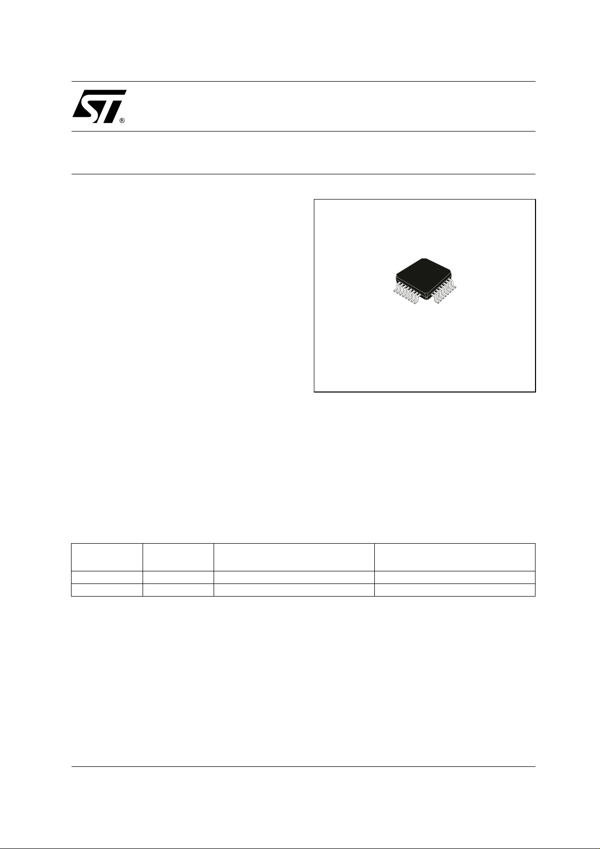
STLVD111
TQFP32
DESCRIPTION
The STLVD111 is a low skew program mable 1 to
10 differential LVDS driver, designed for clock
distribution. The select signal is fanned out to 10
identical differential outputs.
The STLVD111 is provided with a 11 bit shift
register with a serial in and a Control Register.
The purpose is to enable or power off each output
clock c hannel and to s elect the clock input . The
produced with low skew as the key goal. Optimal
design and layout serve to minimize gate to gate
skew within a device. The net result is a
dependable guaranteed low skew dev ice.
The STLVD111 can be used for high performanc e
clock distribution in 2.5V systems with LVDS
levels. Designers can take adv antage of the
device’s performance to d istribute low skew
clocks across the backplane or the board.
STLVD111 is s pec ific ally designed, modelled and
ORDERING CODES
Type
STLVD111BF -40 to 85 °C TQFP32 (Tray) 250 parts per Tray
STLVD111BFR -40 to 85 °C TQFP32 (Tape & Reel) 2400 parts per reel
Temperature
Range
Package Comments
1/12December 2002
Page 2
STLVD111
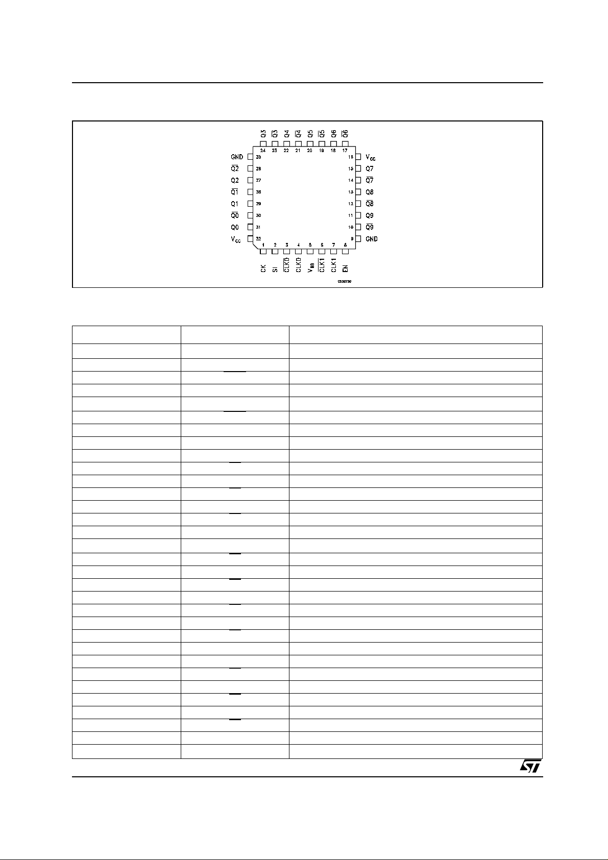
PIN CONFIGURATION
PIN DESCRIPTION
PlN N° SYMBOL NAME AND FUNCTION
1 CK Control Register Clock
2 SI Control Register Serial IN/CLK_SEL
3 CLK0
4 CLK0 Differential Input
5
6 CLK1
7 CLK1 Differential Input
8 EN Device Enable/Program
9 GND Ground
10 Q9
11 Q9 Differential Outputs
12 Q8
13 Q8 Differential Outputs
14 Q7
15 Q7 Differential Outputs
16
17 Q6
18 Q6 Differential Outputs
19 Q5
20 Q5 Differential Outputs
21 Q4
22 Q4 Differential Outputs
23 Q3
24 Q3 Differential Outputs
25 GND Ground
26 Q2
27 Q2 Differential Outputs
28 Q1
29 Q1 Differential Outputs
30 Q0
31 Q0 Differential Outputs
32
2/12
Differential Input
V
BB
Output Reference Voltage
Differential Input
Differential Outputs
Differential Outputs
Differential Outputs
V
CC
Supply Voltage
Differential Outputs
Differential Outputs
Differential Outputs
Differential Outputs
Differential Outputs
Differential Outputs
Differential Outputs
V
CC
Supply Voltage
Page 3
STLVD111
ABSOLUTE MAXIMUM RATINGS
Symbol Parameter Value Unit
V
V
V
I
OSD
ESD Electrostatic Discharge (HBM 1.5KΩ, 100pF)
Absolute Maximum Ratings are those values beyond which damage to the device may occur. Functional operation under these condition is
not implied.
THERMAL DATA
Symbol Parameter Value Unit
R
RECOMMENDED OPERATIN G CONDITIONS
Symbol Parameter Min TYP Max Unit
V
CC
V
IC
T
A
T
Supply Voltage
CC
Input Voltage -0.2 to (VCC+0.2)
I
Output Voltage -0.2 to (VCC+0.2)
O
Driver Short Circuit Current
-0.3 to 2.8 V
Continuous
>2 KV
Thermal Resistance Junction-Case
Tj-c
Supply Voltage
2.375 2.625 V
13 °C/W
Receiver Common Mode Input Voltage 0.5(VID) 2-0.5(VID)
Operating Free-Air Temperature Range
Operating Junction Temperature
J
-40 85 °C
-40 105 °C
V
V
V
DRIVER ELECTRICAL CHARACTERISTICS (T
= -40 to 85 °C, VCC= 2.5V ± 5%, unless otherwise
A
specified (Note 1, 2)
Symbol Parameter Test Conditions
Min. Typ. Max.
V
∆V
V
∆V
NOTE 1: All currents into device pins are positive; all currents out of device pins are negative. All voltages are referenced to device ground
unless otherwise specified.
NOTE 2: All typical values are given for V
Output Differential Voltage
OD
(Fig. 2)
ODVOD
OS
OSVOS
I
OS
Magnitude Change 30 mV
Offset Voltage -40 ≤ TA≤ 85°C 1.05 1.15 1.25 V
Magnitude Change 30 V
Output Short Circuit Current VO=0V 15 30 mA
RL=100Ω 400 500 600 mV
=0V 7 15
V
OD
=2.5VandTA= 25°C unless otherwise stated.
CC
Value
Unit
RECEIVER ELECTRICAL CHARACTERISTICS (TA=-40to85°C,VCC= 2. 5V ± 5%, unless otherwise
specified (Note 1, 2)
Symbol Parameter Test Conditions
Min. Typ. Max.
V
V
NOTE 1: All currents into device pins are positive; all currents out of device pins are negative. All voltages are referenced to device ground
unless otherwise specified.
NOTE 2: All typical values are given for V
Input Threshold High 100 mV
IDH
Input Threshold Low -100 mV
IDL
Input Current VI= 0V 42 100 µA
I
IN
=0V
V
I
CC
=2.5VandTA= 25°C unless otherwise stated.
CC
Value
Unit
210
3/12
Page 4
STLVD111
DRIVER ELECTRICAL CHARACTERISTICS (TA= -40 to 85 °C, VCC= 2.5V ± 5%, unless otherwise
specified (Note 1, 2)
Symbol Parameter Test Conditions
Unit
Min. Typ. Max.
Value
Output Reference Voltage VCC= 2.5 V 1.15 1.25 1.35 V
V
BB
I
C
NOTE 1: All currents into device pins are positive; all currents out of device pins are negative. All voltages are referenced to device ground
unless otherwise specified.
NOTE 2: All typical values are given for V
Power Supply Current All driver enabled and loaded 125 160 mA
CCD
Input Capacitance VI=0VtoV
C
IN
Output Capacitance 5 pF
OUT
Logic Input High Threshold VCC= 2.5 V 2 V
V
IH
V
Logic Input Low Threshold VCC= 2.5 V 0.8 V
IL
Logic Input Current VCC= 2.5 V, VIN=VCCorGND ±10 µA
I
I
=2.5VandTA= 25°C unless otherwise stated.
CC
CC
5pF
LVDS TIMING CHARACTERISTICS (TA= -40 to 85 °C, VCC= 2.5V ± 5%, unless otherwise specified
(Note 4)
Symbol Parameter Test Conditions
Min. Typ. Max.
t
TLH,tTHL
t
PHL,tPLH
f
MAX
t
SKEW
Transition Time RL= 100 Ω,CL= 5 pF, Fig. 5, 6) 220 300 ps
Propagation Delay Time (Fig. 5, 6) 2 2.5 ns
Maximum Input Frequency 700 900 MHz
Bank Skew (Fig. 1) 50 ps
Part to Part Skew (Fig. 2) 100
Pulse Skew (Fig. 3) 50
NOTE 4: Generator waveforms for all test conditions: f=1MHz, ZO=50Ω(unless otherwise specified).
Value
Unit
CONTROL REGISTER TIMING CHARACTERISTICS (TA=-40to85°C,VCC= 2.5V ±5%,EN=H, unless
otherwise specified (Figure 4)
Symbol Parameter Test Conditions
f
MAX
t
Maximum Frequency of Shift
(Fig. 7) 100 150 MHz
Register
Clock to SI Setup Time (Fig. 7) 2 ns
t
s
Clock to SI Hold Time (Fig. 7) 1.5 ns
t
h
Enable to Clock Removal Time (Fig. 7) 1.5 ns
rem
Minimum Clock Pulse Width (Fig. 7) 3 ns
t
W
4/12
Min. Typ. Max.
Value
Unit
Page 5

STLVD111
SPECIFICATION OF CONTROL REGISTER
The STLVD111 is provided with a 11 bit shift register with a Serial In and a Control Register. The purpose
is to enable or power o f each output clock channel and to select the clock input. The STLVD111 provides
two working modality:
PROGRAMMED MODE (EN=1)
The shift register have a serial input to load the working configuration. Once the configuration is load ed
with 11 clock pulse, another clock pulse load the configuration into the control register. The first bit on the
serial input line enables the outputs Q9 and Q9
The last bit is the cloc k selection bit. To restart the configuration of the s hift register a reset of the state
machine must be done with a clock pulse on CK and the EN set to Low. The c ont rol register shift register
can be configured on time after each reset.
STANDARD MODE (EN=0)
In Standard Mode the STLVD111 isn’t programmable, all the c lock o utputs are enabled. The LVDS clock
input is selected from Clock 0 or Clock 1 with the S I pin as shown in the Truth Table below.
TRUTH TABLE OF STATE MACHINE INPUTS
EN SI CK OUTPUT
L L X All Output Enabled, Clock 0 selected, Control Register disabled
L H X All Output Enabled, Clock 1 selected, Control Register disabled
HL
HH
LX
, the second bit enab les the outputs Q8 and Q8 and so on.
First stage stores "L", other stages store the data of previous stage
First stage stores "H", other stages store the data of previous stage
Reset of the state machine, Shift register and Control Register
SERIAL INPUT S EQUENCE
BIT#10 BIT#9 BIT#8 BIT#7 BIT#6 BIT#5 BIT#4 BIT#3 BIT#2 BIT#1 BIT#0
CLK_SEL Q0 Q1 Q2 Q3 Q4 Q5 Q6 Q7 Q8 Q9
TRUTH TABLE OF THE CONTROL REGISTER
BIT#10 BIT#(0-9) Qn(0-9)
L H Clock 0
H H Clock 1
X L Qn Output Disabled
TRUTH TABLE
CK EN SI CLK 0 CLK 0
LLLLHXXLH
LLLHLXXHL
L L L Open Open X X L H
LLHXXLHLH
LLHXXHLHL
L L H X X Open Open L H
All drivers enable
CLK 1 CLK 1 Q (0-9) Q(0-9)
5/12
Page 6

STLVD111
LOGIC DIAGRAM
6/12
Page 7

STLVD111
Figure1 : BANK SKEW - t
sk(b)
Figure2 : PART TO PART SKEW - t
sk(PP)
Figure3 : PULSE SKEW - t
t
: BANKSKEW is the magnitude of the time difference between outputs with a single driving input terminal
sk(b)
t
: PART TO PART SKEW is the magnitude of the difference in propagation delay times between any specific terminals of two devices
sk(pp)
when both devices operate with the same input signals, the same supply voltages, and the same temperature, and have identical packages
and test circuits.
tsk(b): PULSE SKEW is the magnitude of the time difference between the high to low and low to high propagation delay times at an output.
sk(P)
7/12
Page 8

STLVD111
Figure4 : VOLTAGE AND CURRENT DEFINITION
Figure5 : TEST CIRCUIT AND V OLTAGE DEFINITION FOR THE DIFFERENTIAL OUTPUT SIGNAL
8/12
Page 9

STLVD111
Figure6 : DIFFERENTIAL RECEIVER TO DRIVE PROPAGATION DELAY AND DRIVE TRANSITION
TIME WAVEFORMS
Figure7 : SET-UP, HOLD AND THE REMOVAL TIME, MAXIMUM FREQUENCY, MINIMUM PULSE
WIDTH WAVEFORMS
9/12
Page 10

STLVD111
TQFP32 MECHANICAL DATA
DIM.
mm. inch
MIN. TYP MAX. MIN. TYP. MAX.
A 1.6 0.063
A1 0.05 0.15 0.002 0.006
A2 1.35 1.40 1.45 0.053 0.055 0.057
B 0.30 0.37 0.45 0.012 0.015 0.018
C 0.09 0.20 0.0035 0.0079
D 9.00 0.354
D1 7.00 0.276
D3 5.60 0.220
E 0.80 0.031
E 9.00 0.354
E1 7.00 0.276
E3 5.60 0.220
L 0.45 0.60 0.75 0.018 0.024 0.030
L1 1.00 0.039
K 0˚3.5˚7˚ 0˚3.5˚7˚
D
D1
A1
1724
25
B
32
1
e
8
TQFP32
16
L1
E
L
K
E3D3E1
9
0.10mm
.004
Seating Plane
B
A
A2
C
0060661/C
10/12
Page 11

STLVD111
Tape & Reel TQFP32 MECHANICAL DATA
mm. inch
DIM.
MIN. TYP MAX. MIN. TYP. MAX.
A 330 12.992
C 12.8 13.2 0.504 0.519
D 20.2 0.795
N 60 2.362
T 22.4 0.882
Ao 9.5 9.7 0.374 0.382
Bo 9.5 9.7 0.374 0.382
Ko 2.1 2.3 0.083 0.091
Po 3.9 4.1 0.153 0.161
P 11.9 12.1 0.468 0.476
11/12
Page 12

STLVD111
Information furnished is believed to be accurate and reliable. However, STMicroelectronics assumes no responsibi lity f or the
consequences of use of such informatio n nor for any infringement of paten ts or o ther rig hts of t hird part ies which ma y result from
its use. No license is granted by implication or otherwise under any patent or patent rights of STMicroelectronics. Specifications
mentioned in this publication are subject to change without notice. This publication supersedes and replaces all information
previousl y suppl ied. STM icroel ectronics produc ts are not auth orized for use as c ritica l compone nts in l ife s upport dev ices or
systems without express written approval of STMicroelectronics.
Australia - Brazil - Canada - China - Finland - France - Germany - Hong Kong - India - Israel - Italy - Japan - Malaysia - Malta - Morocco
© The ST logo is a registered trademark of STMicroelectronics
© 2002 STMicroelectronics - Printed in Italy - All Rights Reserved
STMicroelectronics GROUP OF COMPANIES
Singapore - Spain - Sweden - Switzerland - United Kingdom - United States.
© http://www.st.com
12/12
 Loading...