

Page 1
查询STM1001供应商
FEAT URES SUMMARY
■ PRECISION MONITORING OF 3V, 3.3V, and
5V SUPPLY VOLTAGES
■ OPEN DRAIN RST OUTPUT
■ 140ms RESET PULSE WIDTH (MIN)
■ LOW SUPPLY CURRENT - 6µA (TYP)
■ GUARANTEED RST ASSERT ION DOWN TO
= 1.0V
V
CC
■ OPERATING TEMPERAT UR E:
–40°C to 85°C (Industrial Grade)
■ LEAD-FREE, SMALL SOT 2 3 PACK AGE
STM1001
Reset Circuit
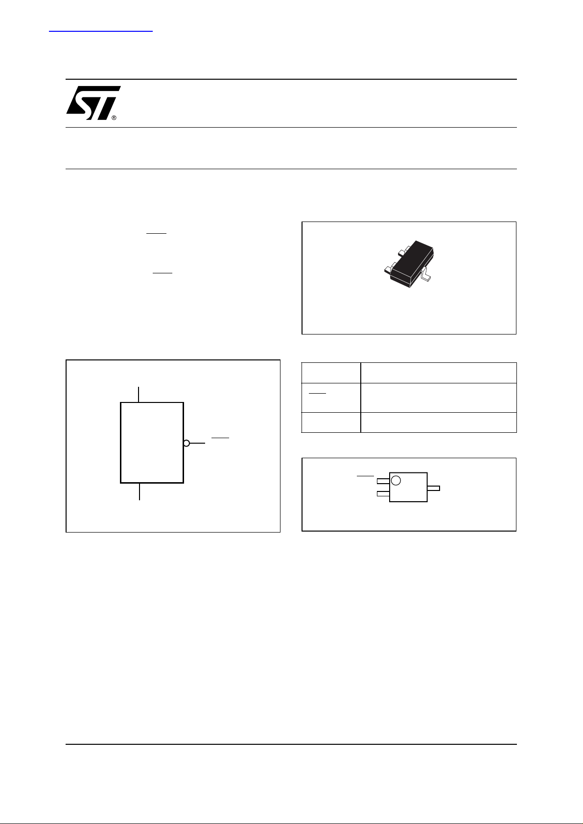
Figure 2. Package
SOT23-3 (WX)
Figure 1. Logic Diagram
V
CC
STM1001
V
SS
RST
AI09116
Table 1. Signal Names
V
SS
RST
V
CC
Ground
Active-Low RESET Output (Open
Drain)
Supply Voltage
Figure 3. SOT23-3 Connections
CC
1
3
2
AI09117
RST
V
V
SS
1/13November 2004
Page 2

STM1001
TABLE OF CONTENTS
FEATURES SUMMARY . . . . . . . . . . . . . . . . . . . . . . . . . . . . . . . . . . . . . . . . . . . . . . . . . . . . . . . . . . . . . 1
Figure 1. Logic Diagram . . . . . . . . . . . . . . . . . . . . . . . . . . . . . . . . . . . . . . . . . . . . . . . . . . . . . . . . . . 1
Figure 2. Package. . . . . . . . . . . . . . . . . . . . . . . . . . . . . . . . . . . . . . . . . . . . . . . . . . . . . . . . . . . . . . . 1
Table 1. Signal Names . . . . . . . . . . . . . . . . . . . . . . . . . . . . . . . . . . . . . . . . . . . . . . . . . . . . . . . . . . 1
Figure 3. SOT23-3 Connections. . . . . . . . . . . . . . . . . . . . . . . . . . . . . . . . . . . . . . . . . . . . . . . . . . . . 1
SUMMARY DESCRIPTION. . . . . . . . . . . . . . . . . . . . . . . . . . . . . . . . . . . . . . . . . . . . . . . . . . . . . . . . . . . 3
Figure 4. Block Diagram . . . . . . . . . . . . . . . . . . . . . . . . . . . . . . . . . . . . . . . . . . . . . . . . . . . . . . . . . . 3
Figure 5. Hardware Hookup . . . . . . . . . . . . . . . . . . . . . . . . . . . . . . . . . . . . . . . . . . . . . . . . . . . . . . . 3
OPERATION . . . . . . . . . . . . . . . . . . . . . . . . . . . . . . . . . . . . . . . . . . . . . . . . . . . . . . . . . . . . . . . . . . . . . . 4
Reset Output . . . . . . . . . . . . . . . . . . . . . . . . . . . . . . . . . . . . . . . . . . . . . . . . . . . . . . . . . . . . . . . . . . 4
Negativ e- Go in g V
Valid /RST Output Down to V
TYPICAL OPERATING CHARACTERISTICS . . . . . . . . . . . . . . . . . . . . . . . . . . . . . . . . . . . . . . . . . . . . 5
Figure 6. Supply Current vs. Temperature, L/M/R/S/T (no load) . . . . . . . . . . . . . . . . . . . . . . . . . . . 5
Figure 7. Power-down Reset Delay vs. Temperature - V
Figure 8. Power-down Reset Delay vs. Temperature - V
Figure 9. Power-up t
Figure 10.Normalized Reset Threshold vs. Temperature . . . . . . . . . . . . . . . . . . . . . . . . . . . . . . . . . 7
Figure 11.Max Transient Duration NOT Causing Reset Pulse vs. Reset Comparator Overdrive . . . 7
Transients . . . . . . . . . . . . . . . . . . . . . . . . . . . . . . . . . . . . . . . . . . . . . . . . . . . 4
CC
= 0V. . . . . . . . . . . . . . . . . . . . . . . . . . . . . . . . . . . . . . . . . . . . . . . 4
CC
= VTH – VCC (L/M). . . . . . . . . . . . . . . .5
OD
= VTH – VCC (R/S/T) . . . . . . . . . . . . . . 6
OD
vs. Temperature . . . . . . . . . . . . . . . . . . . . . . . . . . . . . . . . . . . . . . . . . . . . . 6
rec
MAXIMUM RATING. . . . . . . . . . . . . . . . . . . . . . . . . . . . . . . . . . . . . . . . . . . . . . . . . . . . . . . . . . . . . . . . . 8
Table 2. Absolute Maximum Ratings. . . . . . . . . . . . . . . . . . . . . . . . . . . . . . . . . . . . . . . . . . . . . . . . 8
DC and AC PARAMETERS . . . . . . . . . . . . . . . . . . . . . . . . . . . . . . . . . . . . . . . . . . . . . . . . . . . . . . . . . . 8
Table 3. Operating and AC Measurement Conditions. . . . . . . . . . . . . . . . . . . . . . . . . . . . . . . . . . . 8
Figure 12.AC Testing Input/Output Waveforms. . . . . . . . . . . . . . . . . . . . . . . . . . . . . . . . . . . . . . . . . 8
Table 4. DC and A C Characteristics . . . . . . . . . . . . . . . . . . . . . . . . . . . . . . . . . . . . . . . . . . . . . . . .9
PACKAGE MECHANICAL . . . . . . . . . . . . . . . . . . . . . . . . . . . . . . . . . . . . . . . . . . . . . . . . . . . . . . . . . . 1 0
Figure 13.SOT23-3 – 3-lead Small Outline Transistor Package Outline. . . . . . . . . . . . . . . . . . . . . 10
Table 5. S OT 23-3 – 3-lead Small Outline Transi stor Package Mechani ca l Data . . . . . . . . . . . . . 10
PART NUMBERING . . . . . . . . . . . . . . . . . . . . . . . . . . . . . . . . . . . . . . . . . . . . . . . . . . . . . . . . . . . . . . . 11
Table 6. Ordering Information Scheme . . . . . . . . . . . . . . . . . . . . . . . . . . . . . . . . . . . . . . . . . . . . . 11
Table 7. Marking Description . . . . . . . . . . . . . . . . . . . . . . . . . . . . . . . . . . . . . . . . . . . . . . . . . . . . . 11
REVISION HISTORY . . . . . . . . . . . . . . . . . . . . . . . . . . . . . . . . . . . . . . . . . . . . . . . . . . . . . . . . . . . . . . . 12
Table 8. Document Revision History . . . . . . . . . . . . . . . . . . . . . . . . . . . . . . . . . . . . . . . . . . . . . . . 12
2/13
Page 3
SUMMARY DESCRIPTION
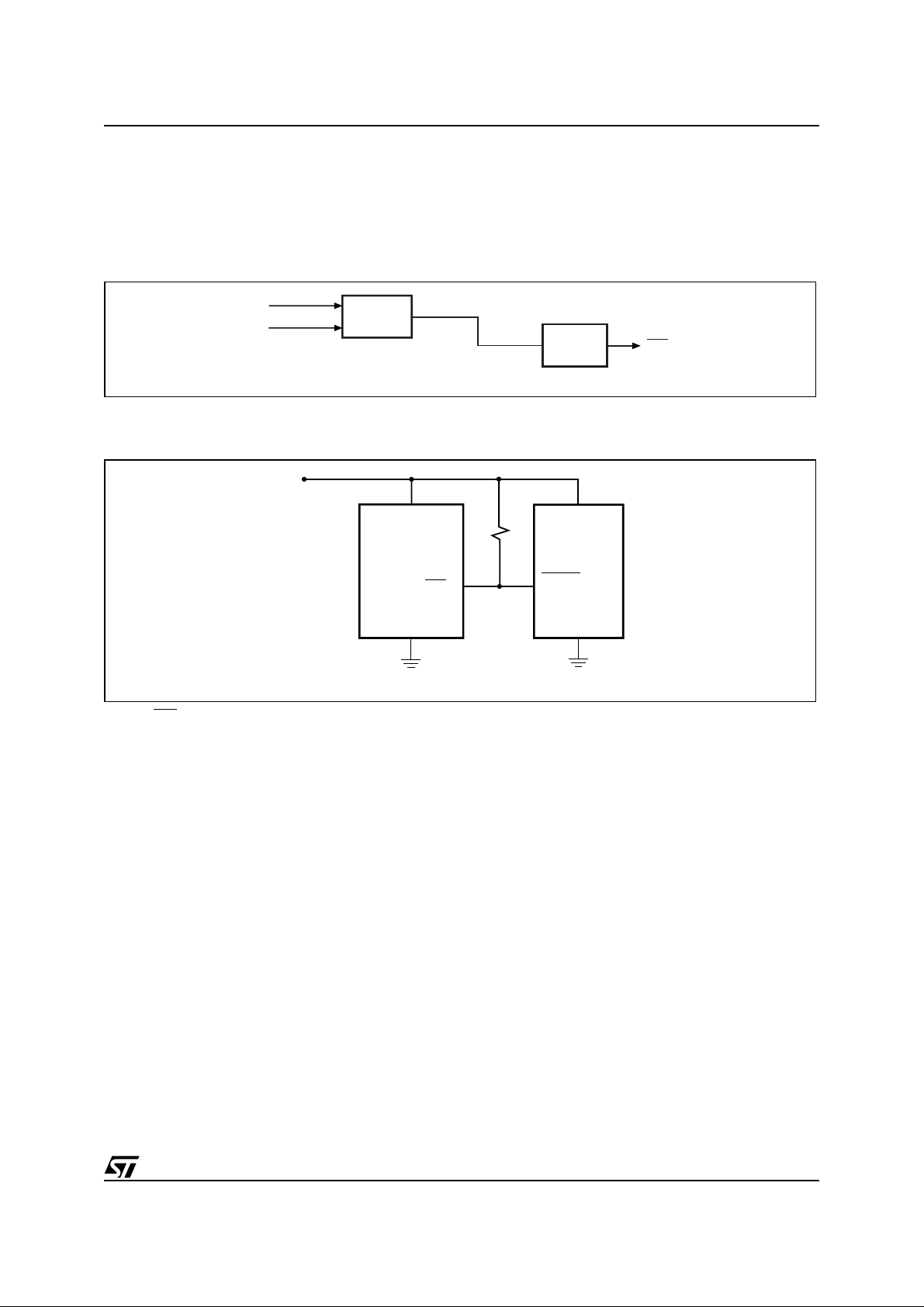
The STM1001 MICROPR OCESSOR RESET Circuit is a low-power supervisory device used to
monitor power supplies. It perf orms a sin gle func tion: asserting a reset signal whenever the V
Figure 4. Block Diagram
V
CC
Note: 1. Ope n Drain
AI09118
V
RST
COMPARE
Figure 5. Hardware Hookup
V
CC
CC
STM1001
supply voltage drops below a preset value and
keeping it asserted until V
preset threshold for a minimum period of time
(t
).
rec
t
rec
Generator
has risen ab ove the
CC
(1)
RST
Note: 1. RST output requires pull-up resistor.
V
CC
STM1001
RST
V
SS
V
MCU
RESET
Input
CC
V
SS
AI09119
(1)
(1)
3/13
Page 4

STM1001
OPERATION
Reset Output
The STM1001 MICROPROCESSOR RESET
CIRCUIT asserts a reset signal to the MCU whenever V
RST
70°C).
During power-up, once V
threshold an internal timer keeps RST
reset time-out period, t
returns high.
If V
low. Each time RST
least the reset time-out period. Any time V
below the reset threshold, the internal timer clears.
The reset timer starts when V
reset threshold. The active-low reset (RST
open drain output.
Negative-Going V
The STM1001 is relatively immune to negative-going V
shows typical transient duration versus reset comparator overdrive (for which the STM1001 will
NOT generate a reset pulse). The graph was generated using a negative pulse applied to V
starting at 0.5V above the actual reset thre shold
goes below the reset threshold (V
CC
RST
is guaranteed valid down to VCC=1V (0° to
exceeds the reset
CC
low for the
. After this interval, RST
rec
drops below the reset threshold, RST goes
CC
is asserted, it stays low for at
goes
CC
returns above the
CC
) is an
Transients
CC
transients (glitches). Figure 11., page 7
CC
CC
and ending below it by the magnitude indicated
(comparator overdrive). The graph indicates the
).
maximum pulse width a negative V
can have without causing a reset pulse. As the
magnitude of the transient increases (further below the threshold), the maximum allowable pulse
width decreases. Any combination of duration and
overdrive which lies under the curve will NOT generate a reset signal. Typically, a V
CC
goes 100mV below the reset threshold and lasts
20µs or less will not cause a reset pulse. A 0.1µF
bypass capacitor mounted as close as possible to
the V
Valid /RST Output Down to V
When V
pin provides additional transient immunity.
CC
= 0V
CC
falls below 1V, the RST output no long-
CC
er sinks current, but becomes an open circuit. In
most systems this is not a problem, as most MCUs
do not operate below 1V. However, in applications
where RST
output must be valid down to 0V, a
pull-down resistor may be added t o hold the RST
output low. This resistor must be large enough to
not load the RST
to pull the output to ground. A 100KΩ re sistor is
,
recommended.
output, and still be small enough
transient
CC
transient that
4/13
Page 5
STM1001
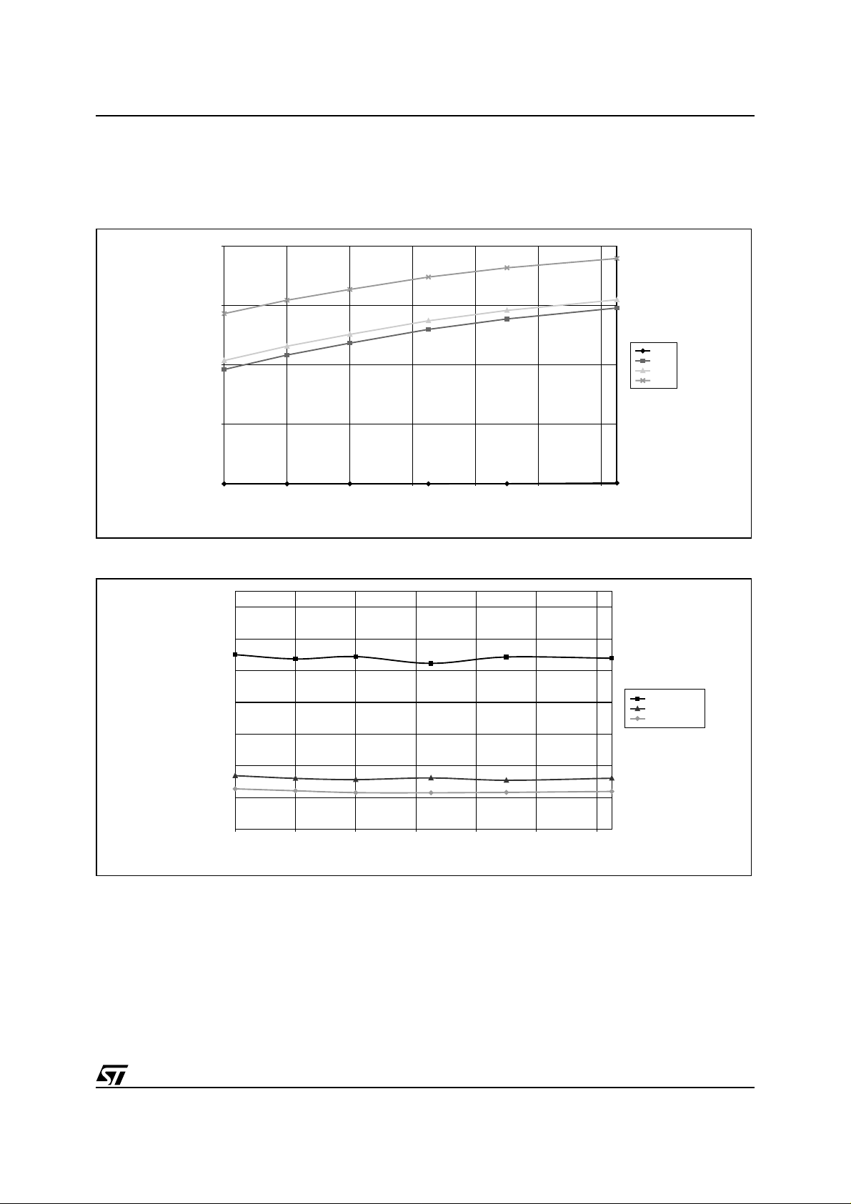
TYPICAL OPERATING CHARACTERISTICS
Note: Typical values are at TA = 25°C, VCC = 5V for L/M versions, VCC = 3.3V for T/S versions, and VCC=
3.0V for R versions.
Figure 6. Supply Current vs. Temperature, L/M/R/S/T (no load)
8.0
6.0
1V
4.0
Supply Current (µA)
2.0
0.0
–40–200 20406080
Temperature (˚C)
AI07879
3V
3.6V
5.5V
Figure 7. Power-down Reset Delay vs. Temperature - V
140.00
120.00
100.00
80.00
60.00
40.00
Power-Down Reset Delay (µs)
20.00
0.00
–40 –20 0 20 40 60 80
Temperature (˚C)
= VTH – VCC (L/M)
OD
AI07880
VOD = 20mV
VOD = 125mV
VOD = 200mV
5/13
Page 6
STM1001
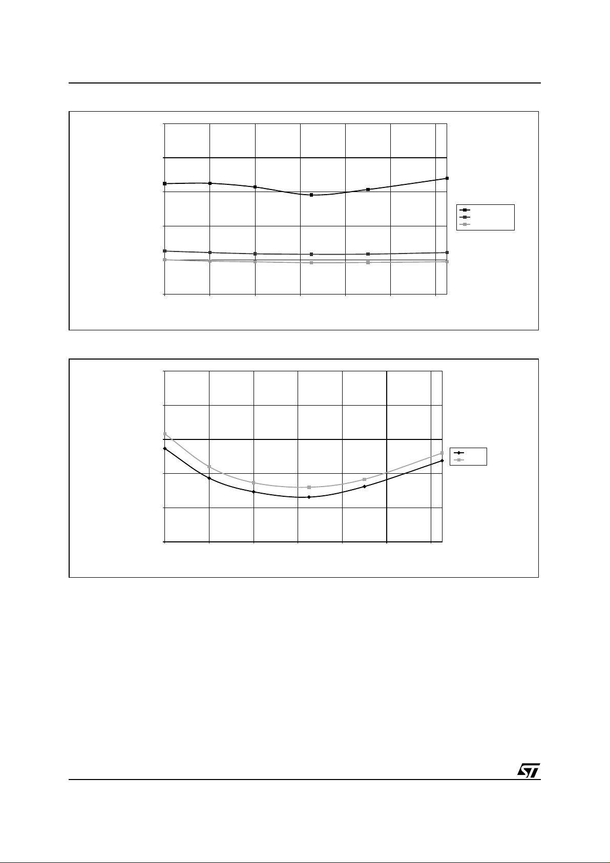
Figure 8. Power-down Reset Delay vs. Temperature - VOD = VTH – VCC (R/S/T)
100.00
80.00
60.00
40.00
20.00
Power-Down Reset Delay (µs)
0.00
–40 –20 0 20 40 60 80
Temperature (˚C)
AI07878
VOD = 20mV
VOD = 125mV
VOD = 200mV
Figure 9. Power-up t
250.00
240.00
230.00
(ms)
rec
220.00
Power-up t
210.00
200.00
–40 –20 0 20 40 60 80
vs. Temperature
rec
Temperature (˚C)
AI07881
L/M
R/S/T
6/13
Page 7
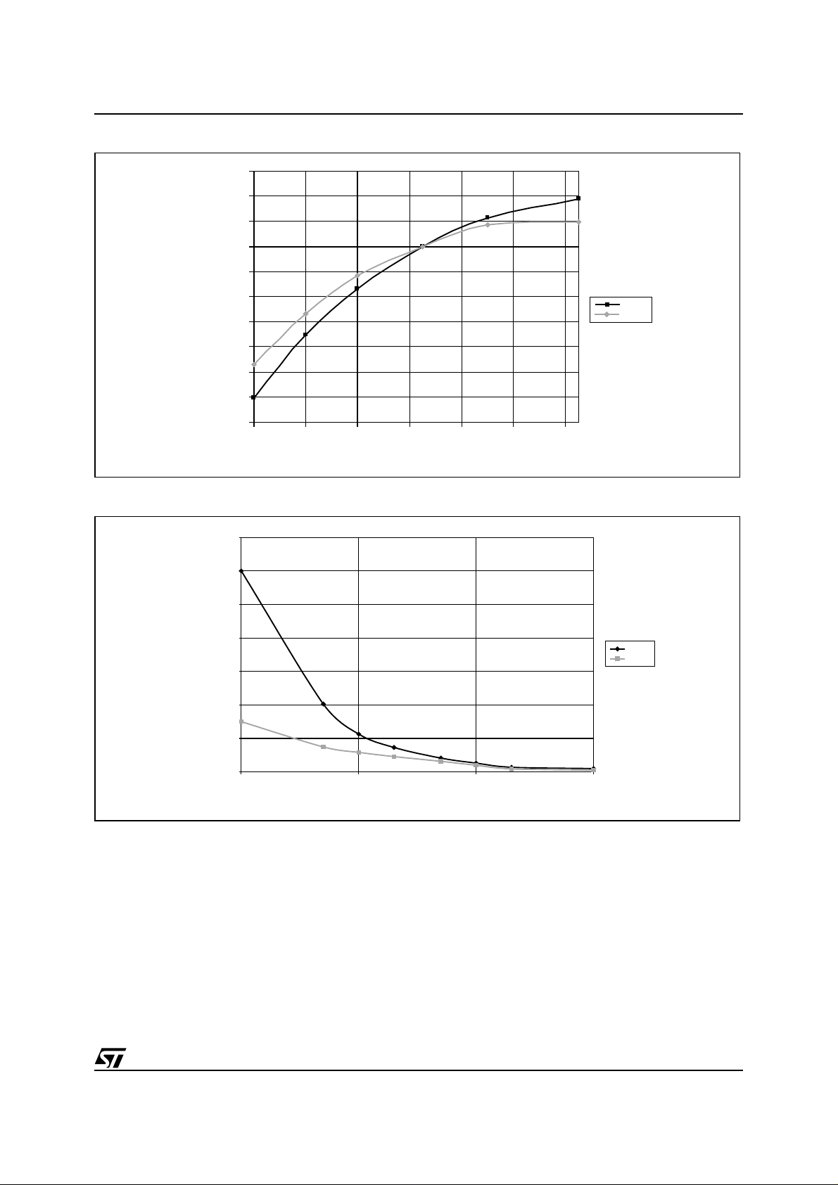
Figure 10. Normalized Reset Threshold vs. Temperature
1.003
1.002
1.001
1.000
0.999
STM1001
0.998
0.997
0.996
Normalized Treshold
L/M
R/S/T
0.995
0.994
0.993
–40 –20 0 20 40 60 80
Temperature (˚C)
AI07882
Figure 11. Max Transient Duration NOT Causing Reset Pulse vs. Reset Comparator Overdrive
700.00
600.00
500.00
400.00
300.00
200.00
R/S/T
L/M
100.00
Maximum Transient Duration (µs)
0.00
1 10 100 1000
Reset Comparator Overdrive, V
– VCC (mV)
RST
AI07883
7/13
Page 8
STM1001
MAXIMUM RA T ING
Stressing the device above the rating listed in the
Absolute Maximum Ratings” table may cause permanent damage to the device. These are stress
ratings only and operation of the device at t hese or
any other conditions ab ove those i ndicated in t he
Operating sections of this specificat ion is not im-
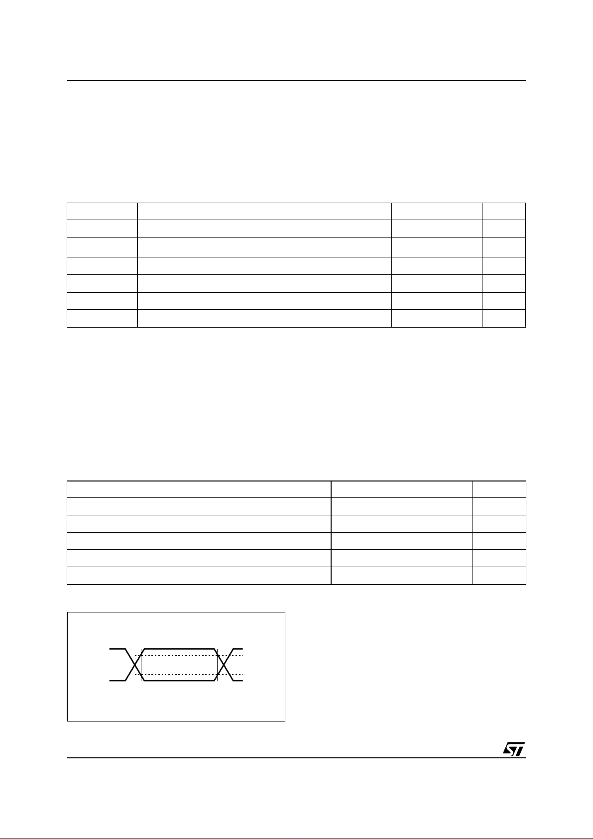
Table 2. Absolute Maximum Ratings
Symbol Parameter Value Unit
plied. Exposure to Absolute Maximum Rating conditions for extended periods may affect device
reliability. Refer also to the STMicroelectronics
SURE Program and other relevan t quality documents.
T
STG
(1)
T
SLD
V
IO
V
CC
I
O
P
D
Note: 1. Reflow at peak temp erature of 255° C to 260°C for < 30 seconds (total thermal budget not to exceed 180°C for between 90 to 150
seconds).
Storage Temperature (VCC Off)
Lead Solder Temperature for 10 seconds 260 °C
Input or Output Voltage
Supply Voltage –0.3 to 7.0 V
Output Current 20 mA
Power Dissipation 320 mW
–55 to 150 °C
–0.3 to V
CC
+0.3
V
DC AND AC PARAMETERS
This section summarizes t he operating m easurement conditions, and the DC and AC characteristics of the device. The parameters in the D C and
AC characteristics Tables that follow, are derived
from tests performed under the Measurement
Table 3. Operating and AC Measurement Conditions
Parameter STM1001 Unit
V
Supply Voltage
CC
Ambient Operating Temperature (T
Input Rise and Fall Times ≤ 5ns
Input Pulse Voltages
Input and Output Timing Ref. Voltages
)
A
Conditions summarized in Table 3, Operating and
AC Measurement Conditions. Designers should
check that the operating cond itions in their circuit
match the operating conditions when relying on
the quoted parameters.
1.0 to 5.5 V
–40 to 85 °C
0.2 to 0.8V
0.3 to 0.7V
CC
CC
V
V
Figure 12. AC Testing Input/Output Waveforms
0.8V
8/13
0.2V
CC
CC
0.7V
0.3V
AI02568
CC
CC
Page 9
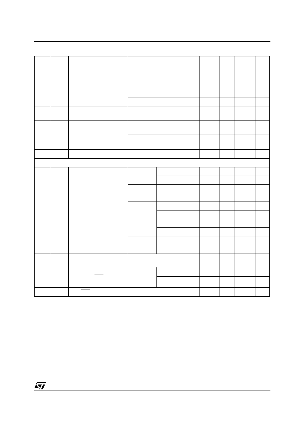
Table 4. DC and AC Characteristics
Sym
V
RESET Thresholds
Alter-
native
CC
I
CC
I
LO
V
OL
V
OL
Description
Operating Voltage
VCC Supply Current
Open Drain Reset Output
Leakage Current
RST Output Low Voltage
RST Output Low Voltage
Test Condition
= –40 to +85°C
T
A
= 0 to +70°C
T
A
V
< 3.6V
CC
V
< 5.5V
CC
> V
V
CC
RST
Reset not asserted
STM1001R/S/T only, I
VCC = V
RST
(min)
STM1001L/M only, I
VCC = V
I
= 50µA; VCC > 1.0V
OL
RST
(min)
(1)
,
= 1.2mA
OL
= 3.2mA
OL
STM1001
Min Typ Max Unit
1.2 5.5 V
1.0 5.5 V
5.5 10 µA
715µA
–1 +1 µA
0.3 V
0.4 V
0.3 V
STM1001L
25°C 4.56 4.63 4.70 V
–40 to 85°C 4.50 4.75 V
25°C 4.31 4.38 4.45 V
STM1001M
–40 to 85°C 4.25 4.50 V
25°C 3.04 3.08 3.11 V
V
RST
Reset Threshold
STM1001T
–40 to 85°C 3.00 3.15 V
25°C 2.89 2.93 2.96 V
STM1001S
–40 to 85°C 2.85 3.00 V
25°C 2.59 2.63 2.66 V
STM1001R
–40 to 85°C 2.55 2.70 V
V
Temperature
RST
Coefficient
V
to RST Delay
V
CC
CC
to (V
100mV)
t
rec
Note: 1. Vali d fo r Ambient Operating Temperature: TA = –40 to 85°C; VCC = 1.2V to 5.5V (except where no ted).
2. “Glitches” of 100ns or less typically will not generate a RESET pulse.
RST Pulse Width 140 210 280 ms
= V
RST
RST
–
V
= 3.3V
CC
STM1001L/M 40 µs
STM1001R/S/T 20 µs
45
ppm/
C
9/13
Page 10
STM1001
PACKAG E MECHANICAL
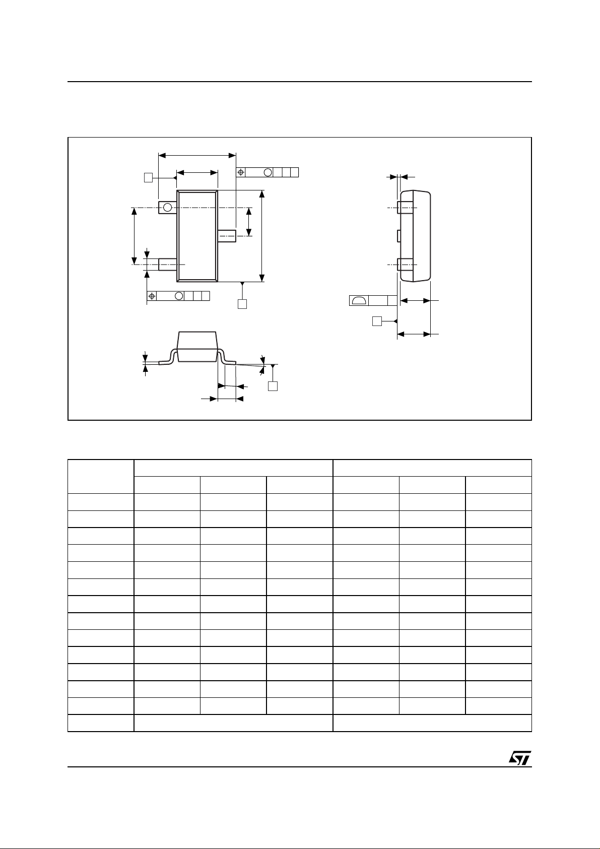
Figure 13. SOT23-3 – 3-lead Small Outline Transistor Package Outline
E
E1
B
1
e1
0.15
e
M
D
CAB
A1
0.20 C A B
3X b
C
M
A
θ
C
L1
3X
0.10 C
C
A2
L
SOT23-3
Note: D rawing is not to scale.
Table 5. SOT23-3 – 3-lead Small Outline Transistor Package Mechanical Data
Symbol
Typ Min Max Typ Min Max
A 0.89 1.12 0.035 0.044
A1 0.01 0.10 0.001 0.004
A2 0.88 1.02 0.035 0.042
b 0.30 0.50 0.012 0.020
C 0.08 0.20 0.003 0.008
D 2.80 3.04 0.110 0.120
E 2.10 2.64 0.083 0.104
mm inches
A
E1 1.20 1.40 0.047 0.055
e 0.89 1.03 0.035 0.041
e1 1.78 2.05 0.070 0.081
L 0.54 0.021
L1 0.40 0.60 0.016 0.024
Θ 0° 8° 0° 8°
N3 3
10/13
Page 11
STM1001
PART NUMBERING
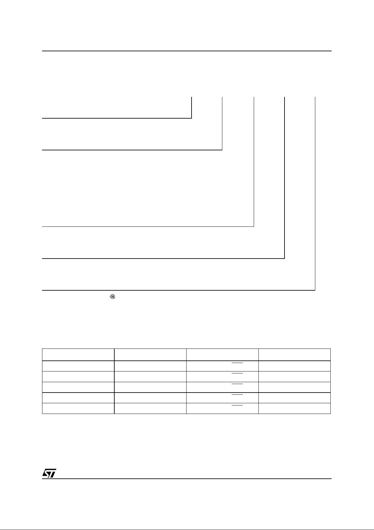
Table 6. Ordering Information Scheme
Example: STM1001 L WX 6 F
Device Type
STM1001
Reset Threshold Voltage
L = V
M = V
T = V
S = V
R = V
Package
WX = SOT23-3
= 4.50V to 4.75V
RST
= 4.25V to 4.50V
RST
= 3.00V to 3.15V
RST
= 2.85V to 3.00V
RST
= 2.55V to 2.70V
RST
Temperature Range
6 = –40 to 85°C
Shipping Method
F = Pb-Free Package (ECO PACK
®
), Tape & Reel
For other options, or for more information on any aspect of this device, please contact the ST Sales Office
nearest you.
Table 7. Marking Description
Part Number Reset Threshold Output
STM1001L 4.63V Open Drain RST 8BAx
STM1001M 4.38V Open Drain RST
STM1001T 3.08V Open Drain RST
STM1001S 2.93V Open Drain RST
STM1001R 2.63V Open Drain RST
Note: 1. Lowercase “x” indicates date code.
Topside Marking
8BBx
8BCx
8BDx
8BEx
(1)
11/13
Page 12

STM1001
REVISION HISTORY
Table 8. Document Revision History
Date Version Revision Details
09-Dec-03 1.0 First Edition
19-Feb-04 2.0 Part number changed from STM6301
22-Mar-04 2.1 Update DC Characteristics (Table 4)
09-Apr-04 3.0 Device promoted; reformatted; markin g updated (Table 7)
19-Nov-04 4.0 Update dimensions (Table 5)
12/13
Page 13

STM1001
Information furnished is believed to be accurate and reliable. However, STMicroelectronics a ssumes no responsibility fo r the c onsequences
of use of such information nor for any infringement of patents or other rights of third parties which may result from its use. No license is granted
by implication or otherwise under any patent or patent rights of STMicroelectronics. Specifications mentioned in this publication are subject
to change without notice. This publication supersedes and replaces all information previously supplied. STMicroelectronics products are not
authori zed for use as criti cal component s in life support devices or sys tems without express written approval of STMicroele ct ronics.
The ST logo is a registered trademark of STMi croelectronics.
All other nam es are the property of their r espective owners
© 2004 STMi croelectroni cs - All rights reserved
Australi a - Belgium - Brazil - Canada - China - Czech Republic - Finl and - France - Germany - Hong Kong - India - Israel - Italy - Japan -
Malaysia - M al ta - Morocco - Singapore - Sp ai n - S weden - Swit zerland - United Kingdom - United States of America
STMicroelectronics group of companies
www.st.com
13/13
 Loading...