

Page 1

■ FULLY MONOLITHIC FIXED FREQUENCY
SMPS
■ THREE LOW SIDE DRIVERS FOR STOP
TAIL AND TURN LED LAMPS ARRAYS
DRIVING
■ PROGRAMMABLE LOW SIDE DRIVER
OVER CURRENT LIMIT PROTECTION
■ UNDER CURRENT DIAGNOSTIC
■ INPUT OVERVOLTAGE PROTECTION
■ VERY LOW STAND-BY CURRENT
■ THERMALPROTECTION WITH
HYSTERESIS
DESCRIPTION
The STLC1, a device realized with the well
established BCD technology, is a fixed f re quenc y
fully monolithic SMPS, with three independent
smart low side driver, p rima rily intended for
automotive rear led lamps driving.
STLC1
LED LAMPS CLUSTER DRIVER
PowerSO-20
The output voltage is set using a simple resistor
divider. Thermal shutdown with hysteresis, input
over-voltage and overcurrent protections give
robust des ign solutions.
TM
SCHEMATIC DIAGRAM
TURN
STOP
TAIL
CNTL
TS -PWM
GND
LMP -OU T
OSCILLATOR
PULSE WIDTH
CONTROLLER
OSC
LAMP
OUTAGE
DETECT
B+
THERMAL
PROTECTION
I
N
P
U
T
CONTOLLER
PWM
COMP
PWM
SWITCH
COMP1
M3
-
+
-
ERRAMP
+
REF
M2
ST - LTL-L
R
s
1.24V
TR -L
P-OUT
FDBK
REF
TR -DRV
M1
ST -DRV
TL - DRV
1/16September 2002
Page 2
STLC1
ABSOLUTE MAXIMUM RATINGS
Symbol Parameter Value Unit
V
V
V
TURN,
V
STOP,
V
TAIL
I
TURN,
I
STOP,
I
TAIL
I
TR-DRV,
I
TL-DRV,
I
ST-DRV
I
LMP-OUT
V
P-OUT
I
P-OUT
T
T
Transient Supply Voltage (load dump)
B+
Operating Supply Voltage
B+
60 V
24 V
TURN, STOP and TAIL input pins voltage VB++ 0.3 V
TURN, STOP and TAIL pins current ± 10 mA
TR-DRV, TL-DRV and ST-DRV pins sink current 1.5 A
LMP-OUT pin sink current
P-OUT DC Voltage
P-OUT pin sink current
Storage Temperature Range
stg
Operating Junction Temperature Range
J
120 mA
60 V
Internally Limited A
-55 to +150 °C
-40 to +125 °C
THERMAL DATA
Symbol Parameter
R
thj-case
R
thj-amb
Thermal Resistance Junction-case
Thermal Resistance Junction-Ambient
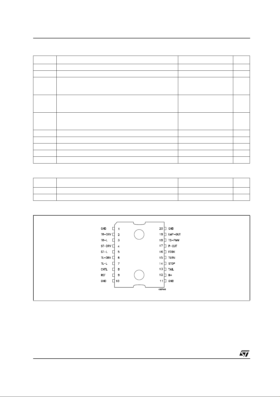
CONNECTION DIAGRAM (t op view)
PowerSO-20
TM
PowerSO-20
TM
2 °C/W
50 °C/W
Unit
2/16
Page 3
PIN DESCRIPTION
Pin N° Symbol Name and Function
1 GND Ground
2 TR-DRV The Low Side Driver drain pin for the TURN LED array
3 TR-L The Low Side Driver source pin, used to detect either a lamp outage or an
over-current condition for the TURN LED array
4 ST-DRV The Low Side Driver drain pin for the STOP LED array
5 ST-L The Low Side Driver source pin, used to detect either a lamp outage or an
over-current condition for the STOP LED array
6 TL-DRV The Low Side Driver drain pin for the TAIL LED array
7 TL-L The Low Side Driver source pin, used to detect either a lamp outage or an
over-current condition for the TAIL LED array
8 CNTL Determines, according to a percentange of VREF,the Pulse Width Controller
internal oscillator duty cycle
9 REF Stable Reference Voltage
10 GND Ground
11 GND Ground
12 B+ Power Supply
13 TAIL TAIL input pin. When brought high, TAIL activates the IC anddrivestheTAIL led
array.
14 STOP STOP input pin. When brought high, STOP activates the IC and drives the
STOP led array.
15 TURN TURN input pin. When brought high, TURN activates the IC and drives the
TURN led array.
16 FDBK Internal Error Amplifier Inverting Pin
17 P-OUT Power MOSFET drain pin
18 TS-PWM A Three State Input. It determine the control logic for TAIL and STOP Low Side
Drivers.
19 LMP-OUT A weak pulled up signal during lamps No Fault condition and an active pulldown
when a Fault condition is detected.
20 GND Ground
STLC1
ORDERING INFORMATION
TYPE
STLC1 STLC1PD
PowerSO-20
TM
3/16
Page 4
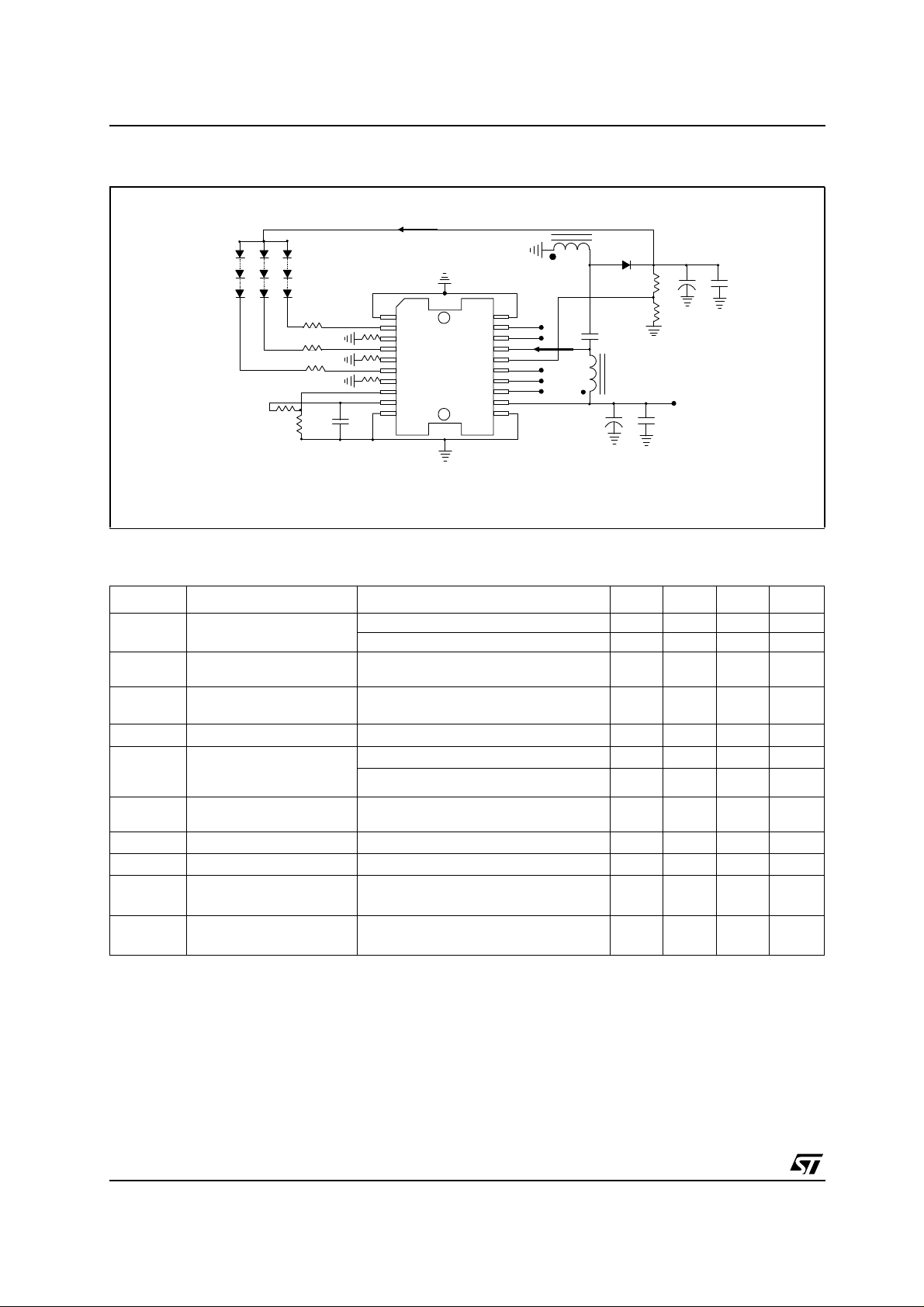
STLC1
TYPICAL APPLICATION CIRCUIT
TURNTAIL
STOP
RC1
RLR
RLS
RLT
RC2
Iout
OUT
C
OUT
RF1
GND
TR-DRV
TR-L
R
TR
ST-DRV
ST-L
R
TS
TL-DRV
TL-L
R
TT
CNTL
REF
C
GND
REF
GND
LMP-OUT
TS-PWM
P-OUT
FDBK
TURN
STOP
TAIL
GND
IP-OUT
B+
RF2
C
SEPIC
ELECTRICAL CHARACTERISTICS FORSMPD SECTION(T
Typical values are referred at T
=25°C, VB+=14V)
J
=-40 to125°C unless otherwise specified.
J
Symbol Parameter Test Conditions Min. Typ. Max. Unit
V
Supply Operating Voltage Normal Operating Range 9 24 V
B+
Normal Operating Range - TAIL only 6 24
V
I
SQ
f
osc
R
P(on)
I
D(off)
I
LIMITIP-OUT
t
SMPS-ON
V
LOAD
V
LINE
B+ Input Overvoltage
SD
Shutdown
Total Off State Quiescent
Current
VB+=14V, V
=0V
TURN=VSTOP=VTAIL
28 30 32 V
120 180 µA
PWM Oscillator Frequency VB+= 14V 140 180 240 kHz
Static drain to ground
SMPS N-channel switch
on resistance
P-OUT Off State leakage
=9V, I
V
B+
=14V, I
V
B+
=4A 180 mΩ
P-OUT
=4A 170 mΩ
P-OUT
VB+= 16V, 20 µA
Current
Current Limit VB+=14V, V
SMPS Turn On Delay C
=1µF (see note 1,4 and Fig 1, 2) 1.6 ms
REF
Load Regulation VB+=14V, I
V
=10V
OUT
Line Regulation VB+= 9 to 16V, I
V
=10V
OUT
= 1V 8 12 16 A
FDBK
= 0.6 to 3A
OUT
OUT
= 1.5A
60 mV
15 mV
4/16
Page 5

STLC1
ELECTRICAL CHARACTERISTICS F OR LOW SIDE DRIVER SECTION (TJ=-40 to 125°C unless
otherwise specified. Typical v alues are referred at T
Symbol Parameter Test Conditions Min. Typ. Max. Unit
R
(on)
I
LSD(off)
t
LSD-ON
V
LS-ON
V
LS-OFF
f
LSD
V
IN(ON)
V
IN(OFF)
Static drain to source LSD
N-channel switch on
resistance
OFF State LSD’S leakage
current
LSD Turn On Delay C
FDBK Voltage over which
LSD’s are enabled
FDBK Voltage over which
LSD’s are disabled
Pulse Width Controller
Internal Oscillator
Frequency
Input Threshold voltage to
enable LSD
Input Threshold voltage to
disable LSD
VB+=9V, V
V
TURN=VSTOP=VTAIL
V
TR-DRV=VST-DRV=VTL-DRV=VB+
=1µFC
REF
(see note 2,4 and Fig 1, 2)
V
TAIL=VB+VTS-PWM=VREF
VB+= 9 to 16V
VB+= 9 to 16V
=25°C, VB+=14V)
J
TURN=VB+VTR-L
I
=1A
TR-DRV
V
STOP=VB+VST-L
I
=1A
ST-DRV
V
TAIL=VB+VTL-L
I
=1A
TL-DRV
=0V
= 220µF
OUT
=0V
=0V
=0V
500 mΩ
500 mΩ
500 mΩ
10 µA
2ms
0.95V
FB
0.5V
FB
/2 200 380 500 Hz
0.6V
B+
0.4V
B+
V
V
V
V
5/16
Page 6

STLC1
ELECTRICAL CHARACTERISTICS F OR FEEDBACK AND CONTROL (TJ=-40 to 125°C unless
otherwise specified. Typical v alues are referred at T
Symbol Parameter Test Conditions Min. Typ. Max. Unit
V
LOUT
V
H-SHORT
V
REF
V
V
LH(en)
V
LH(dis)
V
R
(IN)
T
SHDN
T
HYST
t
F(on)
t
F(off)
V
TS-PWM(L)
V
TS-PWM(M)
V
TS-PWM(H)
Note 1: The device is powered. If only one of the three inputs is enabled (the remaining inputs are shorted to ground), t
required for theOUT voltageto reach the10%of its own steady statevalue
Note 2: The device is powered. If only one of the three inputs is brought high (the remaining inputs are shorted to ground), T
time required for the current to flow in the enabled LSD
Note 3: The device is powered and at least one input is enabled. If this input is disabled, T
come zero in the previously enabled LSD.
Note 4: Guaranteed by design, not tested in production.
Lamp Outage Detect
Threshold Voltage
Output Overcurrent
Threshold Voltage
External Voltage
Reference
Internal Band-gap Voltage
FB
Reference (see schematic
diagram)
Device Enabled Lamp
Outage no fault High
Voltage
Device Disabled Lamp
Outage no fault High
Voltage
Lamp Outage fault Low
LL
Voltage
TURN, STOP and TAIL
Input Resistance
Thermal Shutdown
Threshold
Thermal Shutdown
Hysteresis
Time to Fault Indication
ON
Time to Fault Indication
OFF
TS-PWM Low State
Voltage (see table 1)
TS-PWM Mid State
Voltage (see table 1)
TS-PWM High State
Voltage (see table 1)
TJ=25°C 150 200 250 mV
TJ=25°C 1.2 1.3 1.6 V
V
TURN=VSTOP=VTAIL=VB+
I
=500µA
REF
V
TURN=VSTOP=VTAIL=VB+
VB+= 9 to 16V, I
least one input enabled. No fault
condition.
VB+= 9 to 16V, I
V
TURN=VSTOP=VTAIL
VB+= 9 to 16V I
least one input enabled. Fault condition.
VB+= 12V, 18.5 kΩ
(see Note 4) 150 °C
(see Note 4) 10 °C
=25°C, VB+=14V)
J
LMP-OUT
LMP-OUT
<-4mA At
<-2mA
=0V
LMP-OUT
< 100mA At
3.6 3.8 4 V
1.15 1.24 1.3 V
VB+-2 V
VB+-2 V
1.5 V
60 µs
8ms
0.1V
0.21V
REF
0.98V
REF
is the time required for the current to be-
LSD-OFF
0.79V
SMPS-ON
B+
B+
REF
REF
is the time
LSD-ON
V
V
V
V
V
is the
FUNCTIONAL DESCRIPTION
SMPS
The N-channel Power MOSFET is source
grounded, thus it is possible to use any converter
configuration with the power switch connected to
ground. A SEPIC topology (Single Ended Primary
Inductor Current) is shown in the typical
application schematic.
INPUTS PINS
The IC’s inputs are TURN, STOP and T AIL. If all
inputs are disabled, SMPS and most of the
6/16
internal control and diagnostic circuitry are not
active. This is done in order to maintain the
stand-by quiescent cu rren t at v ery low values.
When only one of these inputs is put high (e.g
connected to V
begins. First the C
), a device start-up phase
B+
capacitor is charged and,
REF
once the voltage on it has reached about 95% of
its steady state value (V
), the SM PS is
REF
enabled. In order to allow the output to reach the
regulated voltage value faster, the LSD
corresponding to the input enabled will conduct
Page 7

STLC1
only when the OUT voltage is about 95% of its
final value. Such a start-up phase takes place
when only one input is enabled.
LOW SIDE DRIVER:
The purpose of the l ow side drivers is to connect
the LED cluste r to ground, creating a path for the
current. U s ing external resistors, current flowing
into the LED cluster is set according to the
following formula:
V
–
OUTVARRAY
I
ARRAY
--------------------------------------------- -=
R
++
TRL
R
on()
where (see typical application schem at ic):
R
L=RLT,RLS
RT=RTT,RTS,orR
R
= Static drain to source LSD on resistance
(on)
= Output Voltage
V
OUT
V
ARRAY
,orR
LR
TR
= Expected LED array voltage drop.
LSD over-current protection and under-current
diagnostic (see LAMP OUTAGE DETECTION
section) is performed by sensing the voltage on
resistors, when the corresponding LSD are
enabled.
If the voltage on exceeds V
H-SHORT
,the
over-current protection acts by reducing the LSD
average current by switching ON and OFF t he
LSD itself.
LAMP OUTAGE DETECTION
Resistors are used to sense the LED array
current. In case one or more LEDs fail (open
circuit) the current on the corresponding resistor
will drop due to the increas ed LED array
resistance. As soon as the voltage drop on is
lower than V
, a LED lamp fault condition is
LOUT
detected and the LMP-OUT pin becomes active
(low). The LAMP-OUT AG E functionality is
AND-ed with each input, that is a fault condition
can be detected only when the LE D arrays are
enabled.
DIMMING
The dimming of the LED lamps can be obt ained by
using the internal PULSE WIDTH controller (it
drives t he LSD TAIL and STOP gates). The duty
cycle of this internal oscillator (whose frequency is
380Hz typical) can be set, forcing the vol tag e of
theCNTLpintobeafractionofV
,byusinga
REF
simple res ist or divider (as shown in the typica l
application scheme).
In this case the duty cycle percentage can be
calculated with the following approximated
formula:
R
3.8 if
≅
DC%
R
C1
---------------------------- 100 E l s ewhere•
R
+
C1RC2
C1
---------------------------R
+
C1RC2
≤
0.2
-------------V
REF
The TS-PWM pin voltage, according to the
TABLE1 determines which LSD is PULSE WIDTH
CONTROLLER driven. Internal dimming c an only
be performed on the T A IL a nd STOP arrays. The
TURN arra y can b e externally dim med (as well as
TAIL and STOP) by driving the corresponding
input witha a square pulse signal whose maximum
frequency must be 200Hz.
7/16
Page 8

STLC1
TS-PWM ENCODING TABLE
TYPE INPUTS ACTIVATED
DRIVE TYPE
TAIL ARRAY STOP ARRY
TAIL PWM PWM
STOP OFF ON
TAIL AND STOP PWM ON
TAIL PWM OFF
STOP OFF ON
TAIL AND STOP PWM ON
TAIL PWM PWM
STOP ON ON
TAIL AND STOP ON ON
(V
TS-PWM
(V
(V
TS-PWM
LOW
TS-PWM
<0.1V
HIGH
<0.1V
MID
/2 or floating)
REF
>0.98V
REF
REF
)
)
Figure1 : S t art-up phase and in put signal t im ing diagram (with TS-PWM floating)
8/16
Page 9

Figure2 : Magnified start-up phase tim ing diagram
STLC1
Figure3 : Fault indication on and off timing diagram
9/16
Page 10

STLC1
TYPICAL CHARACTERISTICS (See PCB BOM)
Figure4 : Output Voltage vs Output Current
Figure5 : Output Voltage vs Output Current
Figure7 : Output Voltage vs Output Current
Figure8 : Duty Cycle Oscillator Frequency vs
CNTL Voltage
Figure6 : Output Voltage vs Output Current
10/16
Figure9 : LMP-OUT Voltage (Fault Condition) vs
LMP-OUT SinkedCurrent
Page 11

STLC1
Figure10 : Total OFF State Quies ce nt Current vs
Temperature
Figure11 : Time to Fault Indication ON vs
Temperature
Figure13 : External Reference Voltage vs
Temperature
Figure14 : V
Voltage vs Temperature
FB
Figure12 : Time to Fault Indication OFF vs
Temperature
11/16
Page 12

STLC1
Figure15 : Demoboard Schematic
Figure16 : PCB Components outline
12/16
Page 13

Figure17 : PBC Top Layer
STLC1
Figure18 : PBC Bottom Layer
13/16
Page 14

STLC1
PCB BOM
REFERENCE DESCRIPTION
L1, L2 VK200
C4, C5, C6 22µF-35V Electrolytic Capacitor Low ESR
C16 220nF-35V Ceramic Capacitor X7R Dielectric
C7 47µF-35V Electrolytic Capacitor
C1, C2 4.7nF-35V Ceramic Capacitor X7R Dielectric
C8, C9 220µF-35V Electrolytic Capacitor Low ESR
C14 560pF
C18 560pF-50V
C11 1µF-35V Tantalium Capacitor
C12 220pF Ceramic Capacitor
R10 9.1kΩ Resistor 125mW 0.1%
R11 1.3kΩ Resistor 125mW 0.1%
R15 4.7kΩ Resistor 125mW 5%
R16 56Ω Resistor 125mW 5%
R18 10Ω Resistor 250mW 5%
R12, R13, R14 1.2kΩ Resistor 125mW 5%
R4, R6, R8 2.2Ω Resistor 1W 5%
R5, R7, R9 1Ω Resistor 1W 5%
TR1 10kΩ Trimmer
RLP 1.5kΩ Resistor 125mW 5%
D1 Schottky Diode STPS3L40S
DLP Led Diode
T1 SEPIC inductor, Toroid Horizontal THT 20µH@10ADC, 200-250KHz
JP1, JP2, JP3 Jumper
14/16
Page 15

PowerSO-20 MECHANICAL DATA
STLC1
DIM.
MIN. TYP MAX. MIN. TYP. MAX.
mm. inch
A 3.60 0.1417
a1 0.10 0.30 0.0039 0.0118
a2 3.30 0.1299
a3 0 0.10 0 0.0039
b 0.40 0.53 0.0157 0.0209
c 0.23 0.32 0.0090 0.0013
D (1) 15.80
16.00
0.6220 0.630
E 13.90 14.50 0.5472 0.5710
e 1.27 0.0500
e3 11.43 0.4500
E1 (1) 10.90 11.10 0.4291 0.4370
E2 2.90 0.1141
G 0 0.10 0.0000 0.0039
h 1.10 0.0433
L 0.80 1.10 0.0314 0.0433
N0˚10˚
1
S0˚ 8˚0˚ 8˚
T 10.0 0.3937
(1) “D and E1” do not include mold flash or protusions - Mold flash or protusions shall not exceed 0.15mm (0.006”)
E2
h x 45˚
NN
a2
b
DETAIL A
110
e3
D
T
e
1120
A
E1
DETAIL B
PSO20MEC
R
Gage Plane
a3
lead
E
DETAIL B
0.35
S
a1
L
c
DETAIL A
slug
-C-
SEATING PLANE
GC
(COPLANARITY)
0056635
15/16
Page 16

STLC1
Information furnished is believed to be accurate and reliable. However, STMicroelect ronics assumes no responsibility for t he
consequences of use of such informatio n nor for any infringement of paten ts or o ther rig hts of t hird part ies which ma y result from
its use. No license is granted by implication or otherwise under any patent or patent rights of STMicroelectronics. Specifications
mentioned in this publication are subject to change without notice. This publication supersedes and replaces all information
previousl y suppl ied. STM icroel ectronics produc ts are not auth orized for use as c ritica l compone nts in l ife s upport dev ices or
systems without express written approval of STMicroelectronics.
Australia - Brazil - Canada - China - Finland - France - Germany - Hong Kong - India - Israel - Italy - Japan - Malaysia - Malta - Morocco
© The ST logo is a registered trademark of STMicroelectronics
© 2002 STMicroelectronics - Printed in Italy - All Rights Reserved
STMicroelectronics GROUP OF COMPANIES
Singapore - Spain - Sweden - Switzerland - United Kingdom - United States.
© http://www.st.com
16/16
 Loading...