

Page 1
■
Wide transmit (~80dB) and receive (~69dB)
dynamic range to limit the external filtering
requirements for extended loop reach operation
■
Programmable tx gain: 0 ÷ -32dB in 2dB steps
■
14-bit D/A converter in transmit path
■
Programmable rx gain: 0 ÷40dB in 0.5dB steps
■
12-bit A/D converter in receive path
■
Integrated phase-locked loop with an externall
LC or crystal oscillator
■
Low power: 300mW @ 5.0V
■
64-pin TQFP package
1.0 GENERAL DESCRIPTION
The STLC1511 G.lite Analog Front End (AFE) chip
implements the analog transceiver functions required
in both a central office modem and a customer
premise modem. It connects the digital modem chip
with the loop driver and hybrid balance circuits. The
STLC1511 has been designed with excellent dynamic range in order to greatly reduce the external filtering requirements at the front end. The AFE chip and
its companion digi tal chip along with a loop driv er, implement the complete G.992.2 DMT modem solution.
STLC1511
NorthenLi te™ G.lite BiCM OS
Analog Front-End Circuit
PRODUCT PREVIEW
TQFP64
ORDERING NUM BER: STLC 1511
The STLC1511 transmit path consists of a 14-bit
Nyquist rate D/A converter, followed by a programmable gain amplifier (TxPGA). The transmit gain is
programmable from 0 to -32dB in 2dB steps.
The STLC1511 receive path contains a buffer amplifier followed by a programmable gain amplifier (RxPGA), a low pass anti-aliasing filter, and a 12-bit
Nyquist rate A/D converter. The RxPGA is digitally
programmable from 0 to 40dB in 0.5dB steps.
2.0 PACKAGING AND PIN INFORMATION
2.1 STLC1511 Pin Allocation
The pinout for the STLC1511 is depicted in Figure 1.
Figure 1. STLC1511 pinout
QVEEDAC
TXDADC1
VEEDAC
VCCDAC
VDDESD2
VSSESD2
VEETXPGA
VCCTXPGA
TXON
TXOP
RXOPINP
VCCRXPGA
QVEETX
48
47
46
45
44
43
42
41
40
39
38
37
36
35
34
33
TQFP64
QVEERX
VEERXPGA
QVEEBIAS
VEEBIAS
VCCBIAS
IREF50m
V3P75V
VCCPLL
VEEPLL
FREQ
OSCNE
OSCNB
OSCPB
OSCPE
VCAP
VDDPLL
VSSPLL
QVEEPLL
RESETN
TXSIN[0]
TXSIN[1]
FRMCLK
VSSDIG1
60
61
62
63
VDDDIG1
CK35M
DIGREF
RXSOUT[0]
RXSOUT[1]
VSSDIGE1
VSSDIG2
VDDDIGE1
VDDDIG2
DTX
DIGCLK
ENB
DRX
VEEADC
VCCADC
QVEEADC
64
1
2
3
4
5
6
7
8
9
10
12
13
14
15
16
17 18 19 20 21
ADCDC3
ADCDC2
59 58 57 56 5455 53 52 51 50 49
22 23 24 25 26
ADCDC1
VSSESD1
RXDCINP
VDDESD1
RXDCON
RXDCINN
RXINN
RXDCOP
271128 29 30 31 32
RXINP
RXOPIINN
November 2000
This is preliminary information on a new product now in development. Details are subject to change without notice.
1/31
Page 2
STLC1511
2.2 Pin Description
Table 1. details the pinout assignment for the
STLC1511. The following list gives the different pin
types for the STLC1511.
■
VDD/VCC - 5V power supply
■
VEE/VSS - Ground supply
■
DO/DI - Digital Output/ Digital Input
■
AO/AI/AIO - Analog Output/ Analog Input/
Analog Input-Output
Table 1. Pin Assignement
Pin # Pin Name Pin Type Pad Type Description
1 VDDDIG1 VDD VDDCO 5V supply (digital) for ADC and DAC
2 CK35M DI TLCHT 35.328MHz serial interface clock input (also used in
Test Mode to test PFD. See Table on page 21)
3 DIGREF DO BT4CR 35.328/17.644MHz reference for Digital ASIC PLL
4 RXSOUT[0] DO BT4CR Rx serial data (lsb) output
5 RXSOUT[1] DO BT4CR Rx serial data (msb) output
6 VSSDIGE1 VSS VSSE Ground for digital output drivers
7 VSSDIG2 VSS VSSCO Ground supply for digital interface, serial interface
8 VDDDIGE1 VDD VDDE
9 VDDDIG2 VDD VDDCO 5 V supply for digital interface, serial interface
5 V supply for digital output drivers
1
10 DTX DO BT4CR Data Output for digital interface
11 DIGCLK DI TLCHT 35.328MHz clock input for digital interface
12 ENB DI TLCHT Enable input for digital interface
13 DRX DI TLCHT Data Input for digital interface
14 VEEADC VEE VSSCO Ground for ADC
15 VCCADC VCC VDDCO 5 V supply for ADC
16 QVEEADC VEE VSSCO Quiet ground for ADC circuitry
17 ADCDC3 AIO ANA ADC reference decoupling (3.75 V) 0.1uF
18 ADCDC2 AIO ANA ADC reference decoupling (2.5 V) 0.1uF
19 ADCDC1 AIO ANA ADC reference decoupling (1.25 V) 0.1uF
20 VSSESD1 VSS VSSA Ground for ESD ring
21 VDDESD1 VDD VDDA 5 V supply for ESD ring
22 RXDCINP AI ANA RxPGA positive input from DC blocking capacitor
23 RXDCINN AI ANA RxPGA negative input from DC blocking capacitor
24 RXDCON AO ANA RxPGA negative output to DC blocking capacitor
25 RXDCOP AO ANA RxPGA positive output to DC blocking capacitor
26 RXINN AI ANA Rx negative input (AC coupled)
27 RXINP AI ANA Rx positive input (AC coupled)
2/31
Page 3
STLC1511
Table 1. Pin Assignement
Pin # Pin Name Pin Type Pad Type Description
28 RXOPINN AI ANA Rx opamp negative input (must be DC coupled)
29 RXOPINP AI ANA Rx opamp positive input (must be DC coupled)
30 VCCRXPGA VCC VDDCO 5V supply for RxPGA
31 VEERXPGA VEE VSSCO Ground for RxPGA
32 QVEERX VEE VSSCO Quiet ground for Rx circuitry
33 QVEEPLL VEE VSSCO Quiet ground for PLL circuitry
34 VSSPLL VSS VSSCO
35 VDDPLL VDD VDDCO
Ground for Oscillator
5 V supply for Oscillator
2
2
36 VCAP AO ANA Charge pump output to varactor
37 OSCPE AIO ANA Oscillator I/O (emitter)
38 OSCPB AIO ANA Oscillator I/O (base)
39 OSCNB AIO ANA Oscillator I/O (base)
40 OSCNE AIO ANA Oscillator I/O (emitter)
41 FREF AI ANA 2.56 MHz PLL input reference/ 35.328 MHz clock
input
42 VEEPLL VEE VSSCO
43 VCCPLL VCC VDDCO
Ground for oscillator
5 V supply for oscillator
2
2
44 V3P75V AIO ANA 3.75V output from Bandgap to 0.22mF capacitor
45
IREF50
m AIO ANA External resistor for bias current R=2.5V/
50mA=50kohm
46 VCCBIAS VCC VDDCO 5V supply for biasing
47 VEEBIAS VEE VSSCO Ground for biasing
48 QVEEBIAS VEE VSSCO Quiet ground for bias circuitry
49 QVEETX VEE VSSCO Quiet ground for Tx circuitry
50 TXOP AO ANA Tx positive output
51 TXON AO ANA Tx negative output
52 VCCTXPGA VCC VDDCO 5V supply for TxPGA
53 VEETXPGA VEE VSSCO Ground for TxPGA
54 VDDESD2 VDD VDDA 5V supply for ESD ring
55 VSSESD2 VSS VSSA Ground for ESD ring
56 VCCDAC VCC VDDCO 5V supply for DAC
57 VEEDAC VEE VSSCO Ground for DAC
58 TXDADC1 AIO ANA DAC reference (2.5V) 0.1uF
3/31
Page 4
STLC1511
Table 1. Pin Assignement
Pin # Pin Name Pin Type Pad Type Description
59 QVEEDAC VEE VSSCO Quiet ground for DAC circuitry
60 RESETN DI TLCHT ResetN for the AFE
61 TXSIN[0] DI TLCHT Tx serial data (lsb) input
62 TXSIN[1] DI TLCHT Tx serial data (msb) input
63 FRMCLK DO BT4CR Tx 4.416MHz frame clock reference output
64 VSSDIG1 VSS VSSCO Ground (digital) for ADC and DAC
<1>H CMOS5 guidelines are fo r 1 pair of power/g r ound for 4 output dr i vers (4 m A)
<2>Pins 35 and 43 are both connected to the analog VCC supplying the on chip oscillator. Similarly, Pins 34 and 42 are connected
to analog VSS for th e oscillato r . Su pply lin e indu ctan ce is re duced u sing two p ads fo r VCC (an d VSS) in this manner. At the board
level, Pins 35 and 43 should be connected to analog VCC, and pins 34 and 42 should be connected to analog VSS.
3.0 FUNCTIONAL DESCRIPTION
3.1 General Functional Desc ription
The STLC1511 consists of the following functional
blocks:
■
Transmit Signal Path
■
Receive Signal Path
■
Phase Lock Loop and Amplifier for an external
oscillator .
■
Bias Voltage and Current Generation
■
Digital Interface
■
Serial Interface
The transmit path contains the 14-bit digital to analog
converter (DAC) necessary to generate the transmit
signal from a 14-bit digital input word. This transmit
signal is then scaled by the on chip programmable
gain amplifier (TxPGA) from 0 to -32dB in 2dB steps.
The scaled output signal is then driven off chip to the
external filters and power amplifier (PA) which drives
the DMT signal to the subscriber loop. The transmit
path is fully differential but may be used single ended
if both outputs from the TxPGA are terminated correctly.
The receive path c ontains an optio nal uni ty gain buffer followed by a two stage programmable gain amplifier (RxPGA), a 1st order low pass anti-aliasing filter,
and a 12-bit analog to digital converter (ADC). The
RxPGA consists of two s tages and the gain i s digitall y
programmable from 0 to 40dB in 0.5dB ste ps. The receive path is fully differential but may be used single
ended provided the other input to the RxPGA is
grounded.
The STLC1511 contains the circuits required to con-
struct a PLL that generates either a 17.644MHz/
35.328 MHz clock from a 2.56 MHz reference clock
when supplied with an external LC or crystal oscillator and tuning circuit. This clock is supplied to the
both the transmit and receive converters, and the serial interface used to transfer the Rx/Tx da ta betw een
the STLC1511 and digital chip. The STLC1511 also
has the ability to be driven directly by an external
35.328MHz clock supplied to the FREF pin.
The bias circuitry contains a bandgap voltage refer-
ence from which the converter references and analog
ground voltage is generated. This block also generates an accurate current using an external resistor
from which all of the S TLC1511 circuits are biased. In
addition, the bias circuitry also generates a 2.5V reference for the external Vco/Vcxo components and
can be used for other external circuits if necessary.
There is a 4 pin serial digital interface (
DIGCLK, ENB
) that loads a one of four 8-bit control
DTX, DR X,
register that controls all the programmable features
on the STLC1511. Refer to “Digital Interface And
Memory Map” on page 20 for more information on
the programmability of the AFE.
To facilitate data transfer between the STLC1511
and the digital ASIC (STLC1510), a 2-bit wide serial
interface for the transmit path and a 2-bit wide serial
interface for the receive path is incorporated into the
AFE. This in terface c onsists of tw o trans mit pins (
SIN[0:1]
), two receive pins (
necessary control signals (
RXSOUT[1:0]
FRMCLK, CK35M
TX-
), and the
) to
transmit the required data. For more information See
“Serial Interface” on page 18.
4/31
Page 5
Figure 2. The block diagram of the STLC1511
50k
0.22uF
V3P5V
IREF50U
0.1uF
TXDADC 1
STLC1511
TX SIN[1:0]
FRM CLK
CK35M
RXS OU T[1:0]
DIGREF
DIGCLK
ENB
DRX
DTX
Band gap/
Bias Gen
2
2
Serial I/F
D igital I/F
RESETN
fp=2M H z
14-bit
DAC
14
4.416M
8/4
35.328M/
17.622M
I/F
dig
2.56M/35.328M
2/3/4/8
PFD
CP
TXON
TXOP
2.56M
(Os c il la t or M od e )
FREF
35.328M
(External Clock Mode)
VCAP
OSCNB
rn
e
t
Ex
Resonator
al
90
OSCPB
5
°
69
G
OSCPE
OSCNE
4.416M
12-bit
ADC
+
-
12
G=1
-
+
+
-
-+
fp=2 M Hz
0.1uF
0.1uF
0.1uF
ADCDC2
ADCDC1
ADCDC3
0.1uF
RXDCOP
RXDCIP
RXDCIN
RXDCO N
0.1uF
+
-
RXINN
RXOPINP
RXOPINN
RXINP
Shaded blocks are only usabe when the PLL is active. Crystal based external resonator for the CPE Mode, LC
based resonator for the CO Oscillator Mode. 35.328 MHz external reference in CO External Clock Mode.
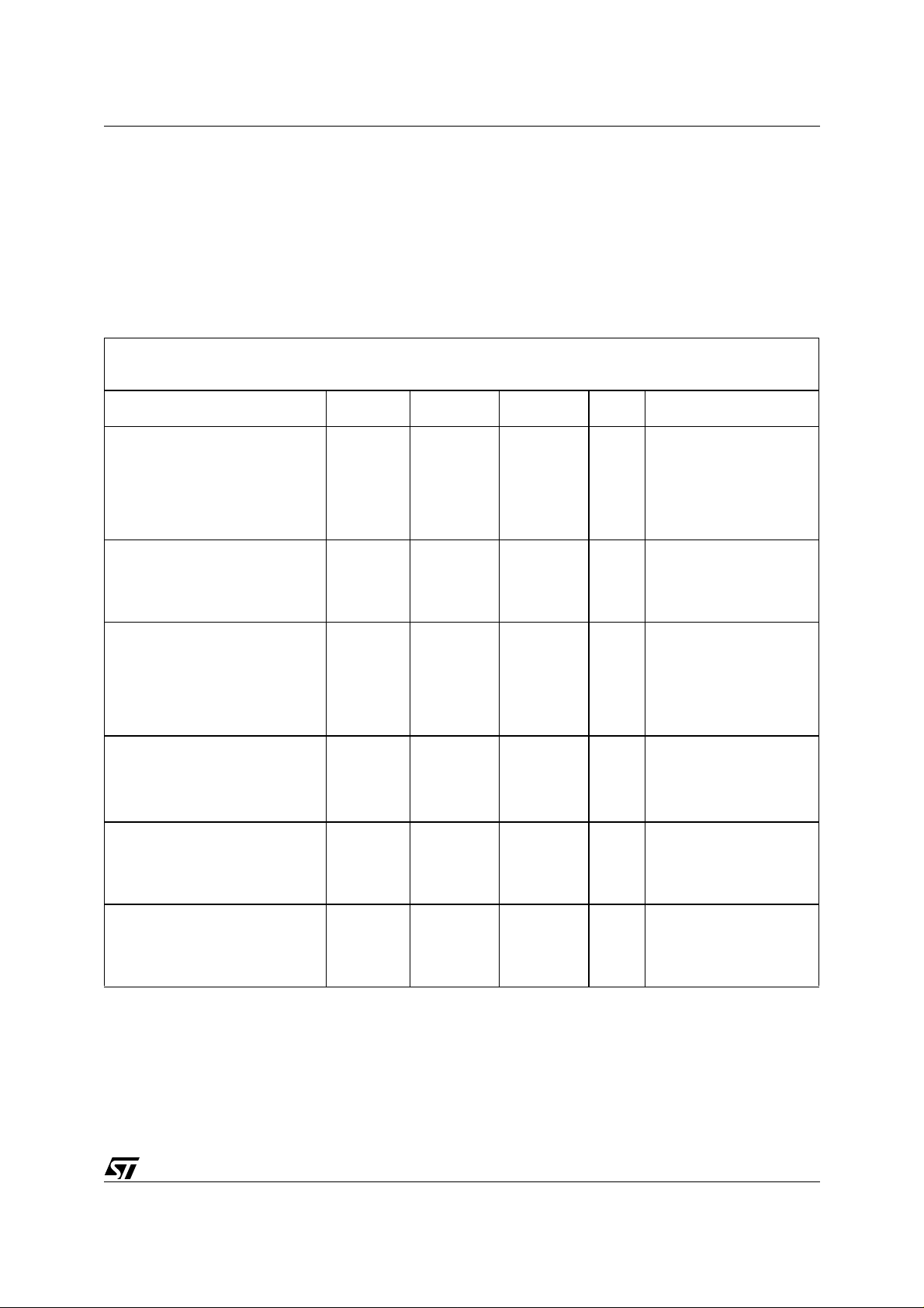
3.2 Receive Path Specifications
Note: The first stage of the RxPGA provides a coarse gain of 0/20dB with a differential input or 6/26dB with a
single ended input. The second stage implements a programmable gain from 0dB to 20dB in 0.5dB steps.
5/31
Page 6
STLC1511
Table 2. Receive Path Specifications
Unless otherwise noted, typical specifications apply for VCC=5.0Volts, temperature=27×C, nominal process and
current. Maximum and minimum performance is with VCC
Description min typ max
1 2
2
0
20
3
6
26
(0.5 · D) - 1.8
18.2
(0.5 · D)
20
1st Stage Absolute Gain1
Diff in to Diff out
3
D = 00
D = 01
Single ended in to Diff out
D = 10
D = 11
2nd Stage Absolute Gain
Diff in to Diff out
4
0 =< D =< 40
D > 40
±5%, -40=<T
(0.5 · D) + 0.8
20.8
junction
=<
105×C, and worst case process.
Units
Comments
Where “D” is the binary
value in b[7:6] of the
dB
control word.
Includes Vcc,
temperature, process,
dB
and frequency variation.
Where “D” is the binary
value in b[5:0] of the
dB
control word.
Includes Vcc,
±
temperature, process,
and frequency variation.
Relative Gain Accuracy
5
(relative to ideal gain of 0.5dB per
LSB change.)
-0.4 +0.4 dB
For more than a 1LSB
change in the control
word.
Assumes a fixed Vcc,
temperature, and
frequency.
Gain Variation with Temperature
Gain Variation with Supply
7
Voltage
Gain Variation with Frequency
8
30kHz =< f =< 120kHz
155kHz =< f =< 540kHz
Gain Step Size
For all steps except step 19.5 to
20dB (differential) or step 25.5 to
26dB (single ended)
For step 19.5 to 20dB
(differential) or step 25.5 to 26dB
(single ended)
6
-0.3 +0.3 dB For a fixed Vcc and
frequency f (30kHz =< f
=< 540kHz) relative to
o
C.
27
-0.1 +0.1 dB For a fixed frequency f.
(30kHz =< f =< 540kHz)
and fixed temperature
relative to Vcc=5.0V.
For a fixed Vcc and
temperature.
-1.0
-1.0
0.4
0.5
0
0
0.6
dB
dB
relative to 30kHz
relative to 155kHz
For a 1 LSB change in
the control word at a
fixed frequency f. (30kHz
=< f =< 540kHz)
0.3
0.5
0.7
dB
6/31
Page 7
Table 2. Receive Path Specifications
STLC1511
Unless otherwise noted, typical specifications apply for VCC=5.0Volts, temperature=27×C, nominal process and
current. Maximum and minimum performance is with VCC
Description min typ max
Input Referred Noise9 10 11
at G=0dB
at G=max
13
12
250
15
±5%, -40=<T
252
19
junction
=<
105×C, and worst case process.
Units
Comments
spot noise @30Khz
measured single ended
nV
at RXINP or RXINN
-----------
Hz
±
spot noise @30kHz
at G=0dB
at G=max
Input Referred Noise
11
9 10 11
at G=0dB
at G=max
Op amp Input Referred Noise
11
9 10 11
Output Signal to Distortion ratio
Two tone (ATE testing)
DS Multi tone
15
14
30kHz =< f =< 120kHz
155kHz =< f =< 540kHz
US Multi-tone
16
30kHz =< f =< 120kHz
155kHz =< f =< 540kHz
60
63
63
63
63
250
20
250
20
10 15
66
69
69
69
69
252
27
252
27
-----------
-----------
dB
measured differentially at
RXINP/N
spot noise @30kHz
measured differentially at
nV
RXDCINP/N
Hz
spot noise @30kHz
nV
measured differentially at
Hz
RXOPINP/N
For all RxPGA gain.
Measured at output of
ADC
Input Impedance
@pins
@ pins
@ pins
RXOPINP/N
RXINP/N
RXDCIP/N
250
1
1
1000
19
10
kW Rx Opamp input pins
Rx PGA input pins
Rx AC coupling pins
DC Offset at output 15 mV measured at output of
ADC
Max Input Signal Level
single ended
differential
1.2
2.4
Vpe
ak
single-ended input
differential input
Vpe
ak
measured at any input
(RXINP/N, RXOPINP/N,
or RXDCINP/N)
Settling Time
17
300
nsec
Time for PGA to settle to
3t accuracy after a
change in the control
word indicated by
ENB
going high.
7/31
Page 8
STLC1511
Table 2. Receive Path Specifications
Unless otherwise noted, typical specifications apply for VCC=5.0Volts, temperature=27×C, nominal process and
current. Maximum and minimum performance is with VCC
±5%, -40=<T
±
junction
Description min typ max
Power Up Time
Rx @ DS
Rx @ US
<1>For the purposes of this specification, a gain of 1 or 0dB is defined as the ratio of the full scale ADC output word to the input voltage
at RXINP/ RXINN when the input t o the Rx path is at 2. 4Vp differ ential measured betw een RXINP and RXINN.
<2>For G.lite the STLC1511 will support both CO and CPE applications. As such it needs to support rates from 30kHz to 120kHz (CO
Receive band) and 155kHz to 540kHz (CPE Receive band).
<3>First stage gain is measured from RXINP/RXINN (differential input) to RXOP/RXON (differential output). Note that the gain from
input to ou tp ut ca n be adj ust ed fo r si ngle ended i nput or di ffe rent ial i nput so tha t the outp ut sign al l evel a t the out put o f the first
stage of the PGA is at full scale. For a single ended input, the unused input, either RXINP or RXINN must be ac coupled to ground.
<4>Second stage gain is me asured from RXDCINP/R XDCINN (differenti al in put) to the out put of the ADC.
<5>Will be tested at Vcc=5.0V, 27
<6>Will be tested at Vcc=5.0V and f=275kHz.
<7>Will be tested at 27
<8>Will be tested at Vcc=5.0V and 27
<9>Due to 1/f component, the spot noise is maximum at 30kHz over the bands of interest (US and DS).
<10>Noise voltage is specified as the noise spectral density (
<11>Input referre d noise assumes that there is a 7dB cut in t he first ba nd of aliased noise whi ch falls i nto the DMT frequencies and
that higher order al i ases are negligi ble. For example, the si ngle ended in put referred noise for th e m aximum gain setting of 40 dB
is calculated as follows:
18
19
20
o
C, and f=275kHz.
o
C and f=275kHz.
o
C.
e
n
PSD 10
1
en 1
-----------------+
10
17nV Hz⁄()
⁄
720
100
530
) at the inpu t. Conversion to power spectral de nsity is as follows
2
en
--------- -
log×=
2
17nV Hz⁄
------------------------------
+
1000×
100
⁄
20 20
10
105×C, and worst case process.
=<
Units
Comments
Time to meet output SNR
mse
requirement
c
2
250nV Hz⁄
----------------------------------
+=
40 20
10
2
⁄
In general , the single ended input referred noise can be calculated as follows:
⁄
.
2
250nV Hz⁄
-------------------------------------
+=
+
()
G1 G2
10
en 1
where G 1 and G2 are the gains of the first and second stages of the RxPGA res pectively. Note that the assumption of a 7dB c ut
on the aliased noise is also used in the above form ul a and that all other higher order noise i s s ufficiently suppressed.
<12>Note that the Rx path noise at 0dB gain is dominated by the quantization noise of the ADC and as such there is very little process,
vcc, or tem perature de pendency and the variati on from typic al to maximum noise is only due to the Rx PG A .
<13>At maximum gain PGA and Rx input opamp noise are the dominant contributors.
<14>Two t one distortion is measured w ith two sinew aves with eac h sinewave at a n amplitude of 1/2 full scale. Tone one is at
f1=400kHz and tone two is at f2=500kHz. The two tone distortion requirement is measured from the rms voltage of a single signal
tone to th e peak rms voltage of the distortion products.
<15>A multi-tone sine wave is used for the DS Multi-tone test. (The multi-tone signal will be 89 sinewaves equally spaced from
36*4.3125kHz to 125*4.3125kHz with a peak-to-rms ratio of 5.3V/V and an rms voltage equal to 1/5.3 of the peak full scale range
of the P GA.) Multi-t one test me asures the di fference between t he rms voltage of a sin gl e tone at the output to the rms vol tage of
the peak distortion product at the output in the band of interest.
<16>A multi-tone sine wave is used for the US Multi-tone test. (The multi-tone signal will be 22 sinewaves equally spaced from
7*4.31 25kHz to 28*4.3125kH z with a peak-to-rm s ratio of 5. 3V/V and an rms vol ta ge equal to 1/5.3 of the peak ful l scale range
of the P GA.) Multi-t one test me asures the di fference between t he rms voltage of a sin gl e tone at the output to the rms vol tage of
the peak distortion product at the output in the band of interest.
<17>The 1t set tling time is roughly equi valent to the unity gain frequency of t he PGA block.
<18>The power up time is the time it takes the power up transient to dissipate such that the output SNR specification is met. This time
is domin ated by the coupling capa citors at pins
-----------------+
10
17nV·Hz⁄()
⁄
710
RXINP/ N
1
2
17nV H z⁄
------------------------------
+
G1 20
10
RXDCIP/N
and
2
⁄
20
8/31
Page 9
STLC1511
<19>Min imum DS f requenc y is 36*4 .3125kH z=155. 25kHz an d as such the coup ling cap acitors b etween
must be such that the high pass pole is ~15kHz (typical). With a 1kW minimum input impedance at
value of about 10nF. This gives a 1t settling time of 10ms.To guarantee 12-bit performance a minimum of 10t settling gives 100ms.
<20>Min imum DS f requenc y is 7*4.31 25kH z=30.18 75kHz an d as such the coup ling cap acitors b etween
must be such that the high pass pole is ~3kHz (typical). With a 1kW minimum input impedance at
value of about 53nF. This gives a 1t settling time of 53ms.To guarantee 12-bit performance a minimum of 10t settling gives 530ms.
RXINP/N
RXDCIP/N
RXINP/N
RXDCIP/N
and
this g ives a ca pacit or
and
this gives a ca pacit or
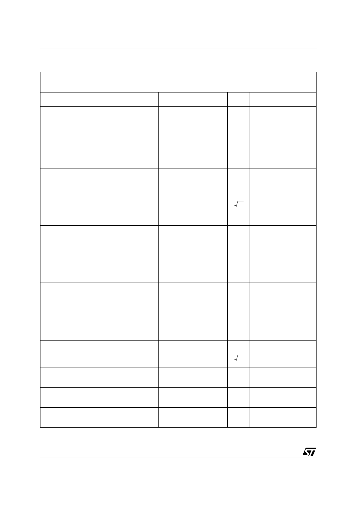
3.3 TRANSMIT PATH SPECIFICATIONS
Table 3. Transmit Path Specifications
Unless otherwise noted, typical specifications apply for VCC=5 Volts, temperature=27×C, nominal process and
current. Maximum and minimum performance is with VCC
Description min typ max
Absolute Gain1
0 =< D =< 16
D > 16
2
-(2 · D) - 1 . 8
-33.8
Gain Step Size 1.8 2.0 2.2 dB For a 1 LSB change in
-(2 · D)
-32.0
±5%, -40 =<T
-(2 · D) - 1.0
-31.0
junction
=<
105×C, and worst case process.
Units
Comments
Where “D” is the binary
dB
value in b[11:7] of the
control word.
Includes Vcc,
temperature, process,
and frequency variation.
the control word at a
fixed frequency f (30kHz
=< f =< 540kHz)
RXDCIP/N
RXDCIP/N
Relative Gain Accuracy
3
(relative to ideal gain of 2dB per
step.)
Gain Variation with Temperature
Gain Variation with Supply
5
Voltage
Gain Variation with Frequency
6
30kHz =< f =< 120kHz
155kHz =< f =< 540kHz
For more than a 1LSB
change in the control
-0.4 +0.4 dB
word.
Assumes a fixed Vcc,
temperature, and
frequency.
4
-0.3 0.3 dB For a fixed Vcc and
frequency f (30kHz =< f
=< 540kHz) relative to
o
C.
27
-0.1 0.1 dB For a fixed frequency f.
(30kHz =< f =< 540kHz)
and fixed temperature
relative to Vcc=5.0V.
For a fixed Vcc and
temperature.
-0.6
-1.0
0
0
dB
relative to 30kHz
relative to 155kHz
9/31
Page 10
STLC1511
Table 3. Transmit Path Specifications
Unless otherwise noted, typical specifications apply for VCC=5 Volts, temperature=27×C, nominal process and
current. Maximum and minimum performance is with VCC
±5%, -40 =<T
junction
=<
105×C, and worst case process.
Description min typ max
Output Signal to Distortion ratio
Two tone
DS Multi-tone
7
8
30kHz =< f =< 120kHz
155kHz =< f =< 540kHz
US Multi-tone
9
30kHz =< f =< 120kHz
155kHz =< f =< 540kHz
Output Referred Noise Voltage
10 11 12
TxPGA Gain = 0dB
30kHz =< f =< 120kHz
155kHz =< f =< 540kHz
TxPGA Gain = min
30kHz =< f =< 120kHz
155kHz =< f =< 540kHz
Output Signal to Noise and
Distortion Ratio (DS)
13 14
TxPGA Gain = 0dB
30kHz =< f =< 120kHz
155kHz =< f =< 540kHz
TxPGA Gain = min
30kHz =< f =< 120kHz
155kHz =< f =< 540kHz
75
78
76
78
78
74
73
53
53
81
84
82
84
84
80
80
30
30
80
79
59
59
100
100
40
40
Units
dB
nV
-----------
dB
Comments
For all TxPGA gains.
Measured differentially at
TXOP/N
measured differentially at
TXOP/N
Hz
measured differentially at
TXOP/N
Output Signal to Noise and
Distortion Ratio (US)
TxPGA Gain = 0dB
30kHz =< f =< 120kHz
155kHz =< f =< 540kHz
TxPGA Gain = min
30kHz =< f =< 120kHz
155kHz =< f =< 540kHz
Out of Band Noise 72 band from 550KHz - 2.2
15 13
76
76
55
55
82
82
61
61
dB
nV
-----------
Hz
measured differentially at
TXOP/N
MHz (f
/2)
S
Maximum Output Signal
@TXOP/N 2.4 Vp differential output
Load Resistance @ pin
TXOP/N
per output to 2.5V
500 W
Load Capacitance @ pin
N
TXOP/
10 pF
per output to 2.5V
10/31
Page 11

STLC1511
Table 3. Transmit Path Specifications
Unless otherwise noted, typical specifications apply for VCC=5 Volts, temperature=27×C, nominal process and
current. Maximum and minimum performance is with VCC
±5%, -40 =<T
junction
105×C, and worst case process.
=<
Description min typ max
Settling Time
16
300 nsec Time for PGA to settle to
Units
Comments
3t accuracy after a
change in the control
word indicated by
going high.
<1>For the purposes of this specification, a gain of 1V/V (i.e. 0dB) is defined as the ratio of the full scale DAC input word to the outpu t
voltage at TXOP/TXON when the ou tput from the T x path is at 2.4Vp di fferenti al m easured bet ween TXOP and T XON.
<2>For G. lit e the STL C15 11 w ill supp ort bot h CO an d C PE ap pli cat ions. As suc h it nee ds to s uppor t ra te s f rom 30kH z to 1 20kHz
(CPE Transmit band) and 155kHz to 540kHz (CO Transmit band). 275kHz is roughly in the middle of the required frequency range.
<3>Will be tested at Vcc=5.0V, 27
<4>Will be tested at Vcc=5.0V and f=275kHz.
<5>Will be tested at 27oC and f=275kHz.
<6>Will be tested at Vcc=5.0V and 27
<7>Two to ne distortion is m easured with two sinew aves with each s inewav e at an amplitude of 1/ 2 full scale. Tone one is at
f1=400kHz and tone two is at f2=500kHz. The two tone distortion requirement is measured from the rms voltage of a single signal
tone to th e peak rms voltage of the distortion prod ucts.
<8>A mult i-tone sine wav e is used for t he DS Multi-ton e test. (The mu lti-tone sign al will be 89 s inewaves equal ly spaced from
36*4.3125kHz to 125*4.3125kHz with a peak-to-rms ratio of 5.3V/V and an rms voltage equal to 1/5.3 of the peak full scale range
of the P GA.) Multi-tone measures the differ ence between the rm s voltag e of a single tone at the out put to the rms vol t age of the
peak distortion product at the output in the band of interest.
<9>A mult i-tone sine wav e is used for t he US Multi-ton e test. (The mu lti-tone sign al will be 21 s inewaves equal ly spaced from
7*4.31 25kHz to 28*4.3125kH z with a peak-to-rm s ratio of 5. 3V/V and an rms vol ta ge equal to 1/5.3 of the peak ful l scale range
of the P GA.) Multi-t one test me asures the di fference between t he rms voltage of a sin gl e tone at the output to the rms vol tage of
the peak distortion product at the output in the band of interest.
<10>Noise voltage is specified as the noise spectral density (
<11>The out put referred noise vol tage for the STLC1511 can be calculated as follows:
o
C, and f=275kHz.
o
C.
PSD 10
e
) at the outpu t. Conversion to power spectral de nsity is as fo llows:
n
2
en
--------- -
log×=
1000×
100
ENB
en 40nV·Hz⁄()
where G is the gain of the TxPGA express ed i n dB .
<12>The output refer red noise of the Tx path at the 0dB gain setting i s mai nly due to t he output r eferred noise of the DA C am plified
by 5.3dB to the output of the chip. The DAC noise itself is made up of roughly equal contributions between quantization noise and
thermal noise. It is only the thermal noise portion which will significantly change between a typical and worst case device.
<13>The S NDR is the r ati o of PS D of the s ign al t o the PS D of the n oise plu s di stort ion. The inp ut for th is tes t is as des c ribe d in
above scaled by the ga in to produce a ful l sc al e output signal.
<14>The ef fective nois e pl us distorti on floor can be calculate d from the SNDR based on the PS D of the output signal
.
2.4 5.3 540kHz 155kHz–×()⁄()
---------------------------------------------------------------------------------------------
PSD 10
So that for G=0, the effective noise plus distortion floor will be at -52.7dBm/Hz - 74dB = -126.7dBm/Hz and for G=max, the floor is
at -52.7dBm/Hz -32dB (cutback) - 53dB = -137.7dBm/Hz
<15>The SNDR is the ratio of PSD of the signal to the PSD of the noise plus distortion. The input for this test is as described in
scaled by t he gain to produce a full scale output sig nal .
<16>1t set tling time is rou ghl y equivalent to the unity g ai n f requency of the PGA block.
log× 52.7dBm Hz⁄–==
2
+=
+
()
G5.3
10
100
⁄
20
50nV·Hz⁄×()
2
2
1000×
i
above
11/31
h
Page 12

STLC1511
3.4 Ph as e Lock Lo op
The STLC1511 has been intended for use in either
the Central Office application (CO) using an external
clock of 35.328MHz, in the Central Office application
using an external 2.56Mhz clock and on-ship PL L , or
in a Customer Premise Equipment application (CPE).
In the CO application (External Clock Mode), the reference clock used for the conver ters and internally in
the STLC1511 is provided by an external reference.
In the CO application (Oscillator Mode), the
STLC1511 provides the ability to drive a LC oscillator
PLL. In the Customer Premise Equipment (CPE) application, the STLC1511 provides the crystal driver
for use with a external crystal and feedback network.
In the CPE application the tuning signal must be provided by the digital modem ASIC (STLC1510).
While the above descriptions highlight the intended
applications, the STLC1511 also has the flexibility to
provide a PLL function when used with a differ ent reference frequency and external 35.328MHz crystal.
Table 4 highlights the different PLL modes for the
STLC1511.
and generate the require clocks using an on-chip
Table 4. PLL Application Modes
Description
CO External Clock Mode
CO Oscillator Mode 2.56 17.664 Yes 88.32 N/A 001001
CPE Mode N/A 35.328 No N/A 35.328 000110
PLL Misc. 1 1.536 35.328 Yes N/A 35.328 011110
2
1
FREF
freq
MHz
35.328 35.328 N o N/A N/A 000000
DIGREF
freq
MHz
PLL
active?
LC Osc
freq
MHz
XT AL
freq
MHz
AFE Control 5
[b5:b0]
PLL Misc. 2 2.048 35.328 Yes N/A 35.328 101110
PLL Misc. 3 4.096 35.328 Yes N/A 35.328 111110
<1>Presently only applications described in this table are supported.
<2>The clock jitter specification for an externally supplied DAC or ADC clock (on pins FREF when in CO External Clock mode) is the
same as the j i tter specification for the PLL.
3.4.1 Central Office (External Clock Mode)
In CO External Clock Mode the 35.328MHz reference clock on pin
FREF
is divided down and used in
both the TX and RX converters. In this mode of operation, the PLL and oscillator driver are powered
down.
External Clock Mode is selected by setting b5:b0 of
register “AFE Control 4” to “000000”. S ee secti on 3.7
for more information.
DIGREF
mode.
details the CO PLL and os cillator performance when
connected as shown in Figure 3, "CO Frequency vs.
Tuning Voltage".
CO Oscillator mode is selected by setting b5:b0 in
register “AFE Control 5” to “001001”. See section
"Digital Interface And Memory Map" on page 20 for
more information.
is running at a rate of 17.664MHz in this
3.4.2 Central Office (Oscillator Mode)
In Oscillator Mode the 2.56MHz reference clock on
FREF
pin
is used as the reference clock for the
STLC1511 PLL. This clock is used to lock the LC oscillator frequency to 88.32MHz which is further divided down to provide the sampling clocks to both the
TX and RX converters and passed to the digital ASIC
STLC1510 as its PLL reference on the pin
DIGREF
.
The clock supplied to the digital ASIC STLC1510 via
12/31
Page 13

STLC1511
Table 5. CO PLL Specifications
Unless otherwise noted, typical specifications apply for VCC=5.0 V, temperature=25×C, nominal process and bias
current. Maximum and minimum performance is with VCC ±5%, -40 =< T
Description min typ max Units Comments
Reference Clock Frequency 2.56 MHz on pin FREF
Output Clock Frequency 17.644 MHz at pin DIGREF
=< 105×C, and worst case process.
junction
LC Frequency Tuning
e
Range
84 88.32 94 MHz Assumes 2% capacitors.
Oscillator Signal Level 200 500 mVp
Power Up Time 200 msec
VCO Gain
Vco gain (LC) 5.0 5.4 6 MHz/V
Charge Pump Current 180 200 220 mA
Input Impedance @OSCPB and
OSCNB
1
Output Impedance @OSCPE
and OSCNE
CO Phase Noise at f
5KHz offset
10kHz offset
20kHz offset
30kHz offset
100kHz offset
200kHz offset
300kHz offset
400kHz offset
500kHz offset
a
2
s
89
dBc/Hz Phase noise at
91
97
101
120
129
133
137
141
see CAPTION FIGURE 4
on page 14
see TITLE 3 3.4.3 on page
16
see TITLE 3 3.4.3 on page
16
DIGREF
output (i.e. 17.664MHz) in
CO Oscillator mode.
<1>Input and output impedance measured with 50kW from OSC P B to Vcc and OSCNB to Vcc
<2>For inband noise, phase noise at multiples of 4.3125kHz will r ms add to degrade the inband SNR. Similarly, for out of b and signals,
phase noise will rms add depen ding on t he offset be tween the c ar rier and the band of interest to reduce the SNR. Fo r e xample,
noise contributions on carriers from 34 to 127 will rms add to degrade the SNR on the edge of the US band (carrier 26).
13/31
Page 14

STLC1511
Figure 3. CO Frequency vs. Tuning Voltage
AFE
Charge Pump
osc_outp
vcc
vcc
osc_outn
Figure 4. CO Frequency vs. Tuning Voltage
VCAP
Ce
I
OSCPE
OSCPB
2.5v
OSCNB
OSCNE
π
C
1n
L
Cv
L
1n
π
C
Ce=100pF
pF
C
π=27
L=56nH
Cv=10pF
Rb=4k
Ω
Rx=1M
Ω
I
Ce
14/31
Page 15

Figure 5. Osc illator Input Impedence
STLC1511
Figure 6. Oscillator Output Impedence
15/31
Page 16

STLC1511
3.4.3 Customer Premise Equipment
In CPE mode, the STLC1511 provides the amplifier
required to power the off-chip crystal oscillator. The
crystal oscillator runs at a frequency of 35.328 MHz
(series resonant) which is further divided down to
provide the sampling clocks to both the TX and RX
converters and passed to the STLC1510 as its PLL
reference on the pin
mode, neither the PLL or the pin
DIGREF
. Note that in CPE
FREF
is us ed (
FREF
should be connected to either Vdd or Vss) and that
the tuing for the external oscillator is generated on
the STLC1510.
The following table details the CPE oscillator performance when connected as shown in Figure 3. on
page 14. CPE mode is selected by setting b5:b0 in
register “AFE Control 5” to “001110”. See section
"Digital Interface And Memory Map" on page 20 for
more information.
Note the reference design provided is based on a
Reeves Hoffman fundamental Mode AT cut crystal at
35.328MHz.(Crystal accuracy@+/-50p pm (+/-15ppm
calibration tolerance, +/-15ppm 10 year aging, +/-20
ppm temperature variation, Rs@15
Ω
max,
Cm@15fF max, and Co@3.5pF typ (assumes a
HC49/43 package).)
Table 6. CPE PLL Specifications
Unless otherwise noted, typical specifications apply for VCC=5.0 V, temperature = 25×C, nominal process and bias
current. Maximum and minimum performance is with VCC ± 5%, -40 =< T
Description min typ max Units Comments
Output Clock Frequency 35.328 MHz at pin DIGREF
Crystal Accurac y
Crystal Frequency Tunin g
2 3
Range
Oscillator Signal Level 200 500 mVp
Power Up Time 5 10 msec
VCO Gain
Vcxo gain (crystal) 1.4 1.6 1.7 KHz/V
Input Impedance @OSCPB
and OSCNB
Output Impedance @OSCPE
and OSCNE
CPE Phase Noise at f
10Hz offset
20Hz offset
40Hz offset
60Hz offset
80Hz offset
100Hz offset
200Hz offset
400Hz offset
600Hz offset
800Hz offset
1000Hz offset
1 2
4
4
5
s
-50 +50 ppm crystal accuracy for CPE.
-125 +125 ppm Occurs at CPE. Assumes
-51.9
-57.9
-63.9
-67.5
-69.9
-71.9
-77.9
-83.9
-87.5
-89.9
-91.9
=< 105×C, and worst case process.
junction
CO is free running
see TITLE 2 3.5 on page 18
see TITLE 3 3.4.3 on page
16
see TITLE 3 3.4.3 on page
16
dBc/Hz Phase noise at DIGREF
output (i.e. 35.328MHz) in
CPE mode.
<1>For the CPE side a crystal oscillator will be used.
<2>50ppm accuracy is divided as ±15ppm for manufacture, ± 15ppm for 10 year drift, a nd ± 20ppm for temperature variation.
<3>Worst case for tuning is when CO is not locked and CPE must retime from CO. Nominally the tuning range for the CO is ±50ppm,
so that if the CO is free running, the CPE m ust tune over the CO inaccuracy and the CP E crystal inac curacy as wel l .
<4>Input and output impedance measured with 50kW from OSC P B to Vcc and OSCNB to Vcc
<5>For inband noise, phase noise at multiples of 4.3125kHz will r ms add to degrade the inband SNR. Similarly, for out of b and signals,
phase noise will rms add depen ding on t he offset be tween the c ar rier and the band of interest to reduce the SNR. Fo r e xample,
noise contributions on carriers from 34 to 127 will rms add to degrade the SNR on the edge of the US band (carrier 26).
16/31
Page 17

Figure 7. Typical CPE Oscill at or Configuration
STLC1511
AFE
osc_outp
I
vcc
osc_outn
vcc
I
Lm
Cm
Co
Rm
Cm =15fF
C
pF
ο=3.5
Rm=15
Ω
Crystal Model
Figure 8. CP E Fr equency vs. Tuning Volta ge
VCAP
OSCPE
OSCPB
2.5v
OSCNB
OSCNE
Ce
C
C
Cv
π
Ce
π
5v
5v
Ce=180pF
C
pF
π=82
Cv= 20pF
Rb=4k
Ω
Rx=1M
Ω
CPE
DIGITAL
ASIC
Current
Output
∆Σ
Clock
Recovery
17/31
Page 18

STLC1511
3.5 Reference Voltages
Table 7. Reference Voltages/Currents
Unless otherwise noted, typical specifications apply for VCC = 5.0 V, temperature=25×C, nominal process and bias
current. Maximum and minimum performance is with VCC ± 5%, -40 =<T
and bias current.
Description min typ max Units Comments
V3P75V Output voltage 3.6375 3.750 3.8625 Volts measured at V3P75V
Output Referred Noise Voltage
at ANG
TXDADC1 Output voltage 2.425 2.5V 2.575 Volts measured at TXDADC1
TXDADC1 Output current 50 mA measured at TXDADC1
External resistor at IREF 49 50 51 kW assume 2%
External capacitor at V3P75V 0.22 mF
3.6 Serial In te rface
The serial interface on the AFE provides for transmission of transmit and receive data between the
STLC1511 and digital modem ASIC. This is accomplished with a two bit wide data stream in each dir ection plus the appropriate clocks. The data for the
transmit path is input to the AFE on the
TXSIN[1:0]
pins and the data for the r eceiv e pat h is output on the
RXSOUT[1:0]
pins.
The serial interface also consists of a 35.328MHz
CK35M
clock (
) which is generated in the STLC1510
and is used to retime the Tx data sent to the
10 measured at V3P75V
the Rx data before it is sent to the digital chip.
A 4.416MHz pulse is als o output from the STLC1511.
This pulse on pin
start of the output and input data words. The alignment of the data to the
low.
A diagram of this interface is show in Figure 11.
Note the MSB of each of the 8-bit registers is trans-
ferred first (MSB = b15/ b7.)
Note that the data word used by the converters is in
2’s complement notation.
=< 105×C, and worst case process
junction
nV
-----------
Hz
FRMCLK
is used to indicate the
FRMCLK
signal is shown be-
STLC1511. It is also used in the STLC15 11 to retime
18/31
Page 19

Figure 9. Serial Interface Block Diagram
STLC1511
TX S IN[1: 0]
FRMCLK
CK35M
RXSOUT[1:0]
CK35M
2
(4 Dff to align data
edges as required)
2
DQ
(x2)
SDATA
CK
2
SOUT
8-bit Shift Register (x2)
8-bit Shift Register (x2)
OUT[15:0]
DQDQ
LD
LD
DATA[15:0]
SDATA
CK
Data[15:0]
SOUT
Out[15:0]
12
to DAC parallel input
(Note : D A C input is
sampled on posedge
CKDAC)
14
(x14)
CKDAC
(4.416MH z Clock from PLL)
DQ
(4.416 M Hz C lock from PLL)
DQ
from ADC parallel output
(Note: ADC output changes
on posedge of CKADC)
12
CKADC
(x12)
DQ
DQ
DQ
14
DQDQ
DQ
FRMCLK
TXSIN[0]
TXSIN[1]
RXSOUT[0]
RXSOUT[1]
CKDAC
CKADC
msba5a12a4a11a3a10a2a9a1a8
lsb
Da ta clocked ou t by
AD C on this edge
3.6.1 ADC Clip Indicator
Normally, the receive signal level is set such that the
input to the STLC1511 plus the RxPGA gain will not
saturate the input to the ADC converter (for maximum ADC input levels).
If the input signal is too large however and causes the
a7 a6
b1
msb
b2
b10b3b9
lsb
b7
b8
b6 b5 b4
Data sampled by
DAC on this edge
ADC to clip, the STLC1511 will report to the digital
chip that a clip has occ urred. This is accomplis hed by
forcing the output data stream supplied to the digital
chip to either “7FFF” hex for an out of range positive
input or to “8000” hex for an out of range negative input. This is highlighted in Figure 10.
19/31
Page 20

STLC1511
Figure 10. Clip Indicator Output.
CK35M
FRMCL K
P o siti ve C l ip
RXSOUT[0]
RXSOUT[1]
RXSOUT[0]
RXSOUT[1]
Bit 0 in the “AFE Status” register is also set to high
when a clip occurs. This bit can be disabled via the
control interface, see Table 8 on page 21 for more
details. This bit is c leared on read. For more infor mation see "Digital Inter face And Mem ory Map" on page
20.
3.6.2 Tx Loop Back
When bit “b1” of register “011” (AFE Control 4) is asserted the data received on the TXSIN[1:0] pins is
converted to parallel and then sent directly to both the
DAC and the RX parallel data input replacing the usual data from the ADC.
This allows a “loop back” to the input TX data from
TXSIN[1:0] to the RXSOUT[1:0] to help the testability
of the serial interface.
3.7 Digital Interface And Memory Map
All parametric specifications in Table 2 on page 6
and Table 3 on page 9 are guaranteed assuming that
the Digital Interface is inactive.
b[7:0]=FF
b[15:8]=7F
Negative Clip
b[7:0]=00
b[15:8]=80
All parametric specifications in Table 2 and Table 3
are guaranteed assuming that the Digital Interface is
inactive. The digital interface operates at a rate of
35.328 MHz. The companion DSP chip, S TLC1510,
sources the 35.328 MHz clock used by the AFE. To
minimize the impact of digital noise on the
STLC1511, this supplied clock is gated, and is only
enabled during data transfers and during reset.
clock does not need to be present in order to reset the chip.
The processor interface consists of four pins: 1) the
35.328 MHz gated clock (DIGCLK); 2) a data in port
for data transfers (DRX); a data out pin for data transfer (DTX); and 4) a chip select pin (ENB).
There are a tot al of 12 bit s which ar e serially transmitted between the STLC1510 and AFE during data
transfers. The gated clock lasts for a duration of 12
clock cycles. This 12 cycle inter action consists of a R/
W bit, a 3 bit address, and a 8 bit data word.
The format for this serial transaction is given below in
Figure 11.
The
Figure 11. Digital Interface Timing Diagram
DIGCK
(35MHz)
ENB
ADDRESS
[a2:a0]
20/31
DRX
DTX
R/W
DAT A[b7:b0] for write access
DATA[b7:b0] for read access
Page 21

STLC1511
During a transaction, the first bit sent to the AFE determines the type of transaction, R/W
sponds to a read transaction while R/W
=”1” corre-
=”0”
corresponds to a write transaction. The next three
bits, address[a2:a0], determine which of the 8 AFE
registers will be accessed (Table 8). This is followed
by the 8-bit data word.
In both Read and Write transactions, bit 0 (
LSB
) of
the serially transferred 8-bit word is clocked from the
data source first (the data source being the external
DSP during Write transactions; the STLC1511 during
Read transactions).
The definition of these fields within the 8-bit word is
Tabl e 8. AFE Register Map Summary
Addr
[a2:a0]
000 STLC1511 Control 1 (Rx
PGA Gain)
001 STLC1511 Control 2 (Tx
PGA Gain)
010 STLC1511 Control 3
(Power Down Reg)
Name D7 D6 D5 D4 D3 D2 D1 D0 Type
Rx PGA Gain RW
not used Tx PGA Gain RW
not used Rx
outlined below in Table 8 and in the detailed register
maps following.
When the voltage on the
RESETN
pin is low, the bits
in the control register will be reset as per defined in
the detailed register maps.
For a write operation, the data on the
DRX
pin is
latched into the STLC1511 on the negative edge of
DIGCLK
the
signal. The data should change state on
the positive edge of the clock.
DTX
For a read operation, the data on the
put on the positive edge of the clock on pin
pin is out-
DIGCLK
Opa
mp
Pow
er
Dow
n
not
use
d
Rx
Pow
er
Dow
n
Tx
Pow
er
Dow
n
RW
.
011 STLC1511 Control 4
(Misc. Control)
100 AFE Contr ol 5
(PLL Control)
101 not used not used
110 not used not used
111 AFE Statu s not used Clip
<1>Presently there is no difference in the oscillator driver between Oscillator Mode and CPE modes so this bit is unused. However,
it may be required in the f uture and sho ul d be program m ed correctl y i n case needed .
not
use
d
not
use
d
DIGREF
Ena
ble
DIV Output
(Test mode)
FREF Mode PLL
Mod
e
PLL
PFD
inpu
t sel
Osc
Mod
1
e
Tx
Loo
p
back
Clock Source
Control
Clip
Indic
ator
ena
ble
Stat
us
RW
R/W
R
21/31
Page 22

STLC1511
Table 9. Detailed Register Map: AFE Control Byte 1
Title: AFE Control 1 (Rx PGA Gain)
Label: Rx Gain Access Type: R/W
Address: 000 Bits Used: 8
Description: Rx PGA Gain Setting
Bit Label Bit(s) Value Bit Description Reset
RX Gain b5-b0 0ŠDŠ 40
DŠ40
RX Gain MSB b7-b6 00
01
10
11
Gain=D*0.5 dB
Gain=20 dB
Gain=0 dB
Gain=20 dB
Gain=6 dB
Gain=26 dB
Table 10. Detailed Register Map: AFE Control Byte 2
Title: AFE Control 2 (Tx PGA Gain)
Label: Tx Gain Access Type: R/W
Address: 001 Bits Used: 5
Description: Tx PGA Gain Setting
Bit Label Bit(s) Value Bit Description Reset
TX Gain b4-b0 0ŠDŠ16
DŠ16
not used b7-b5 000
Gain= -D*2 dB
Gain=-32 dB
Table 11. Detailed Register Map: AFE Control 3
000000
0
00000
Title: AFE Control 3 (Power Down Reg)
Label: Power Down Access Type: R/W
Address: 010 Bits Used: 3
Description: Power Down Register
Bit Label Bit(s) Value Bit Description Reset
Tx Power Down
Rx Power Down
not used b2 0
22/31
1
2
b0 0
b1 0
Power up transmit path
1
1
Power down transmit path
Power up receive path
Power down receive path
1
1
Page 23

Table 11. Detailed Register Map: AFE Control 3
Title: AFE Control 3 (Power Down Reg)
Label: Power Down Access Type: R/W
Address: 010 Bits Used: 3
Description: Power Down Register
Bit Label Bit(s) Value Bit Description Reset
STLC1511
Rx Opamp Power
Down
not used b7-b4 0
<1>During power dow n the Tx serial in te rface is also disabled and T XSCLK is tris tated.
<2>During power dow n the Rx serial i nt erface is also disabled and RXSCLK an d RX SOUT[1: 0] are tristated
b3 0
Power up RxPGA
1
Power down RxPGA
Table 12. Detailed Register Map: AFE Control 4
Title: AFE Control 4 (Misc. Control)
Label: Misc Control Access Type: R/W
Address: 011 Bits Used: 5
Description : M ode Contr ol/Mis c.
Bit Label Bit(s) Value Bit Description Reset
Clip Indicator Enable b0 0
1
Tx Loop back b1 0
1
Clip indicator disabled
Clip indicator enabled
Normal operation
Test mode. Tx data sent to serial I/F is
muxed to Rx input and trasmitted via the
serial I/F
1
1
0
PLL Phase/Freq Input
Select (Test Mode)
DIV Output
(Test Mode only)
not used b7-b5 000
b2
0
1
b3-b4 00
01
10
11
Source of PLL phase-frequency detector
feedback input.
Output of feedback dividers.
Signal on FREF is sent directly to PFD (ref
input) and signal on
directly to PFD (vco input).
normal operation
Output of DIV69 counter is output to
DIGREF pin
Output of DIV2/3/4/8 counter is output to
DIGREF pin
Output of DIV5 counter is output to
DIGREF pin
pin CK35M
is sent
0
0
23/31
Page 24

STLC1511
Table 13. Detailed Register Map: AFE Control 5
Title: AFE Control 5 (PLL Control)
Label: PLL Control Access Type: R/W
Address: 100 Bits Used: 7
Description: PLL Control Register
Bit Label Bit(s) Value Bit Description Reset
Clock Source Control b0-b1 00
01
10
11
OSC Mode
1
b2 0
1
PLL Mode b3 0
1
FREF Mode
2
b5-b4 00
01
10
11
DIGREF Enable b 6 0
1
(CO External Clock Mode.) Output of
clock selection MUX is from
FREF
pin.
This state also powers down the PLL and
oscillator driver.
(CO Oscillator Mode.) Output of clock
selection MUX is from output of divide by
5.
(CPE Mode). Output of clock selection
MUX is from output of oscillator driver.
(Other CPE Mode). Output of clock
selection MUX is from output of oscillator
driver.
(CO Oscillator mode.) AFE is configured
to drive external 88.32MHz LC oscillator.
(CPE mode.) AFE is configured to drive
external 35.328MHz crystal oscillator.
PLL active (PFD,CP active)
PLL Inactive (PFD,CP powered down)
FREF frequency is 2.56MHz
FREF frequency is 1.536MHz
FREF frequency is 2.048MHz
FREF frequency is 4.096MHz
DIGREF
DIGREF
Output pin tristated
Output pin active
00
1
0
00
1
reserved b7 0
<1>Presently there is no difference in the oscillator driver between CO Oscillator and CPE modes so this bit is unused. However, it
may be required in the fu ture and should be program m ed correc tly in case needed.
<2>For FRE F at 2.56MHz ( b5: b4 = “00”), th e compare frequency for the PLL is at 1. 28MHz. For al l ot her FREF modes the com pare
frequency is at 512k Hz.
24/31
Page 25

STLC1511
Table 14. Detailed Register Map:
Title: AFE Control 6 (Misc Control 2)
Label: Misc Control 2 Access Type: R/W
Address: 101 Bits Used: 0
Description:
Bit Label Bit(s) Value Bit Description Reset
not used b7-b0 00000000
Table 15. Detailed Register Map:
Title: not used
Label: Access Type: R/W
Address: 110 Bits Used: 0
Description:
Bit Label Bit(s) Value Bit Description Reset
not used
not used
not used b7-b0 00000000
Table 16. Detailed Register Map: AFE Status
Title: AFE Status
Label: AFE Status Access Type: R
Address: 111 Bits Used: 2
Description: AFE Read only Status
Bit Label Bit(s) Value Bit Description Reset
Clip Status? b0 0
1
not used b7-b2 000000
A/D clip not detected
A/D clip detected
0
25/31
Page 26

STLC1511
3.8 TIMING
Table 17. describes the timing relationships between important signals.
Tabl e 17. Timing
Symbol Parameter
t
SENB
t
HENB
t
SDRX
t
HDRX
t
DDTX
t
SCK35
t
HCK35
t
DRX
t
DFC
t
DDRCK35
t
RDIGREF
t
FDIGREF
ENB falling to DIGCLK rising 1 5 ns
ENB rising to DIGCLK falling 1 5 ns
Data in valid to DIGCLK falling 2 5 ns
DIGCLK falling to Data in hold 2 5 ns
DIGCLK rising to Data out valid 5 10 ns
TXSIN[1:0] valid to CK35M falling 2 5 ns
CK35M falling to TXSIN[1:0] hold 2 5 ns
CK35M rising to RXSOUT[1:0] valid 5 10 ns
CK35M rising to FRMCLK valid 5 10 ns
DIGREF rising to CK35M rising 10 12 20 ns
DIGREF rise time (20% to 80%) 1 2 3 ns
DIGREF fall time (80% to 20%) 1 2 3 ns
Spec
Min
Typ
Spec
1
Max
Unit
s
<1>Load on al l output pads assumed to be < 25pF.This gi ves a delay thr ough the TLCH T pad of approxim ately 5ns.
3.9 POWER UP RESET
When the voltage on the
RESETN
pin is low the bits in the control register will be reset as per the detailed reg-
ister maps in “Digital Interface And Memory Map” on page 20.
In addition, digital ou tput pins,
DTX, FRMCLK
RXSOUT[1:0]
, and
are high impedance. The other digital outputs
are always as defined in Table 1 on page 2.
26/31
Page 27

4.0 PACKAGE INFORMATION, SUPPLY RATINGS, AND OPERATING ENVIRONMENT
4.1 The thermal impedance
The thermal impedance of the package is about 64 °C/W for the following conditions
°
Table 18. Board Assumptions:
PC Board 6 layer, 1oz copper
STLC1511
Ambient Temp erature
Air Flow natural convection
Power Dissipation 300mW
Table 19. Board Assumptions:
PC Board 6 layer, 1oz copper
Ambient Temp erature
Air Flow natural convection
Power Dissipation 300mW
COMMENT ON RELIABILITY:
year reliability is 125
°
C.
The maximum continuous junction temperatur e for this part while meeting 20
4.2 Environmental Conditions
Table 20. Environment conditions
Ta Long-Ter m (Continuous )
85
85
0
C
0
C
0
-40 to +80
C
T
Short-Term
a
<1>Short-term is defined as no greater than 96 consecutive hours and 15 days per year.
1
-40 to +85 0C
4.3 Pow er Supply Inp ut Li m its
Table 21. defines the maximum and minimum power supply requirements to meet specifications as outlined in
section 3.2 and 3.3.
Table 21. Power Supply Limits
Limits
Parameter
min typ
Positive Supply Voltage 4.75 5 5.25 Volts
max
1
Unit Conditions
27/31
Page 28

STLC1511
Table 21. Power Supply Limits
Limits
Parameter
min typ
Tx Powered Up
CO Oscillator mode
CO External Clock mode
CPE mode
Tx Powered Down
CO Oscillator mode
CO External Clock mode
CPE mode
Tx Powered up
CO Oscillator mode
CO External Clock mode
CPE mode
Tx Powered Down
CO Oscillator mode
CO External Clock mode
CPE mode
<1>Maximum current assumes a 7% increase due to process/temperature/Vcc plus the variation in the external 50k resistor (assumed
2%) connected to IREF 50u. For this table the total variation is assumed at 9% .
65
60
65
41
36
41
325
300
325
200
175
200
max
71
66
71
45
39
45
373
347
373
237
205
237
1
Unit Conditions
mA Includes 4mA for
digital supplies and
digital I/O
mW Includes 20mW for
digital supplies and
digital I/O
4.4 Power Supply Noise
Table 22. Power Supply Noise
Noise Band Maximum 5V Supply Noise Spectral Density Max 5V Supply Noise
30kHz < f <
112kHz
146kHz < f <
547kHz
1.4µVrms/rtHz @ 112kHz, rising 6dB per octave f or decreasing
frequency
1.0µVrms/rtHz @ 146kHz, dropping 6dB per octave to
0.25µVrms/rtHz @ 547kHz
(Over noise band)
1.0mVrms
0.30mVrms
4.5 Absolute Maximum Ratings
The following table describes the maximum and minimum voltage ratings
Table 23. Maximum and minimum voltage rati ngs
pin Maximum Minimum
all VCC pins 6.5V -0.5V
all other pins VCC+0.4 -0.4
28/31
Page 29

STLC1511
4.6 Pin DC Electrical Specification
Table 24. General Interface Electrical Characteristics
Parameter Conditio ns Min Typ Max Unit
Iil Low level input current Vi=0V 1 µA
Iih High level input current Vi=Vcc 1 µA
Ioz
<1>The lea ka ge cu rr ents are gen era lly very sm all, < 1nA . Th e v alu e gi ven here, 1m A, is a maxi mum that can oc cur aft er an E SD
Tri-state output leakage
stress.
1
Vo=0V or Vcc 1 µA
BT4CR is a CMOS tristate 4mA output pad buffer with slew rate control.
Table 25. CMOS Output Pad (BT4CR) DC Electrical Characteristics1,
Parameter Conditions Min Typ Max Unit
Vol Low level output voltage Iol=4mA 0.4 V
Voh High level output voltage Ioh=4mA 0.9*Vdd5 Vdd5 V
<1>Char acterized for VCC=3.0 to 3. 6V. This pad must be characterized at VCC=5.0V+-5% and the table updated
<2>Assumes a 200mV voltage drop in both supply lines. This will not be the case in the STLC1511.
Table 26. TTL Input Pad (TLCHT) DC Electrical Characteristics1,
Parameter Co nditions Min Typ Max Unit
Vil Low level input voltage 0.8 V
Vih High level input voltage 2.0 V
2
2
Vilhyst Low level Threshold input falling 0.9 1.45 V
Vihyst High level Threshold input rising 1.4 1.9 V
<1>Char acterized for VCC=3.0 to 3. 6V. This pad must be characterized at VCC=5.0V+-5% and the table updated
<2>Assumes a 200mV voltage drop in both supply lines. This will not be the case in the STLC1511.
29/31
Page 30

STLC1511
4.7 Package
The STLC1511 will be packaged in a 64pin 10x10x1.4mm Thin Quad Flat Pack (TQFP) package.
DIM.
mm inch
MIN. TYP. MAX. MIN. TYP. MAX.
A 1.60 0.063
A1 0.05 0.15 0.002 0.006
A2 1.35 1.40 1.45 0.053 0.055 0.057
B 0.18 0.23 0.28 0.007 0.009 0.011
C 0.12 0.16 0.20 0.0047 0.0063 0.0079
D 12.00 0.472
D1 10.00 0.394
D3 7.50 0.295
e 0.50 0.0197
E 12.00 0.472
E1 10.00 0.394
E3 7.50 0.295
L 0.40 0.60 0.75 0.0157 0.0236 0.0295
L1 1.00 0.0393
K 0°(min.), 7°(max.)
OUTLINE AND
MECHANICAL DATA
TQFP64
D
D1
TQFP64
3348
32
E3D3E1
17
16
E
L1
L
K
0.10mm
Seating Plane
49
B
64
1
e
A
A2
A1
B
C
30/31
Page 31

STLC1511
Information furnished is believed to be accurate and reliable. However, STMicroelectronics assumes no responsibility for the consequences
of use of such information nor for any infringement of patents or other rights of third parties which may result from its use. No license is granted
by implic ation or otherwise under any patent or p at ent rights of STMicroelectronics. Spec i fications mentioned i n this publication are subject
to change without notice. This publication supersedes and replaces all information previously supplied. STMicroelectronics products are not
authorized for use as cri t i cal compone nts in life support device s or systems without express written approval of STMicroel ectronics.
The ST logo is a registered trademark of STMicroelectronics
2000 STMi croelectronics - All Ri ghts Rese rved
Australi a - Brazil - Chin a - Finland - Franc e - Germany - Hong Kong - India - Ita l y - Japan - Malaysi a - Malta - Morocco - Singapore - Spain
STMicroelectronics GROUP OF COMPANIES
- Sweden - Sw itzerlan d - United Kin gdom - U.S.A.
http://www.s t. com
31/31
 Loading...