

Page 1
1.0 GENERAL DESCRIPTION
STMicroelectronics’ STLC1502 is a high performance VoIP processor specially targeted for the time
effective design of I P-Phones and analog gateway
applications bundled with a comprehensive embedded software solution.
When used in the Enterprise LAN IP Phone space,
this device enables t he augmentation and replacement of traditional telephone systems with network
based communications systems running over local
and wide area IP networks. To design an IP phone,
the only other parts required will be an analog interface, some optional Flash memory for upgradable
software and Fast Ethernet physical layer devices.
The ST complete IP Phone reference design includes standards compliant Application Programming Interfaces (APIs), protocol management
software and software development tools.
STLC1502
VOICE OVER IP PROCESSOR
PQFP208
ORDERING NUM BER: STLC 1502
• 16-bit, fixed point 120 MIPs DSP (D950)
• Two 10/100 Base-T Ethernet MACs
• VLAN support
• Ethernet Bridge
•JTAG
• Smart power management
2.0 REFERENCE SOFTWARE FEATURES
Some of the features of the SW provided are:
The STLC1502 also has all the proper interfaces to
be a cost effective soluti on f or Small Gateway applications. ST also offer a complete SW reference design for Small Gateway applications.
Hence, the STLC1502 enables a superior and cost
effective platform development for IP-phones as well
as voice gateway applications, prov i di ng developers
with a low risk, rapid time to market solutio n .
The STLC1502
a ARM7/TDMI MCU and a dual port 10/100 Base-T
switched Ethernet media access control interface
The main characteristics of the STLC1502 IP processor are as follows:
• HCMOS7 technology
• Power supply: Core 2.5 V and I/O: 3.3 V
• Industry standard 32-bit RISC microprocessor
(ARM7/TDMI core)
integrates low power D950 DSP with
.
ARM7/TDMI
• Industry standard Real time OS: VxWorks
• Network Protocol Stack
• TCP/IP, UDP, TFTP, DHCP, HTTP server
• Ethernet/PC communication drivers
• High Level Chip Control
• Stack management
• SNMP (optional)
• Application Specific MIBS
• Signalling Protocol
• MGCP, H.323 (including H.450), SIP
D950 Voice Codec Unit (VCU) features:
• G.711 Packetized PCM
• G.729AB, 8kbps CS-ACELP
• G.726, 16-40 kbps ADPCM
• G.723.1a, 6.3/5.3 kbps MP-MLQ
• Encoding and decoding of PCM sample
frames
• Packing/unpacking of compressed information in Codewords
• Fax Modem : T.38 Fax Relay, V.21, V.17,
V.27ter and V.29 f ax datapump
January 2002
This is preliminary information on a new product now in development. Details are subject to change without notice.
Revision: A04
1/81
Page 2
STLC1502
• Data Modem: V.34 datapump
• Rate selection
• High performance voice activity detector (VA D)
• Comfort noise generator (CNG)
• G.165 32 ms Line & acoustic echo canceller
• Low latency system implementation
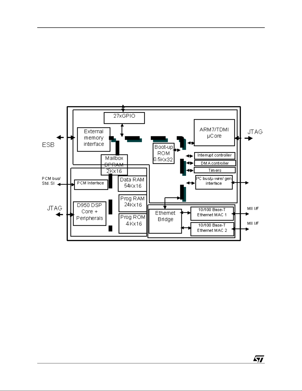
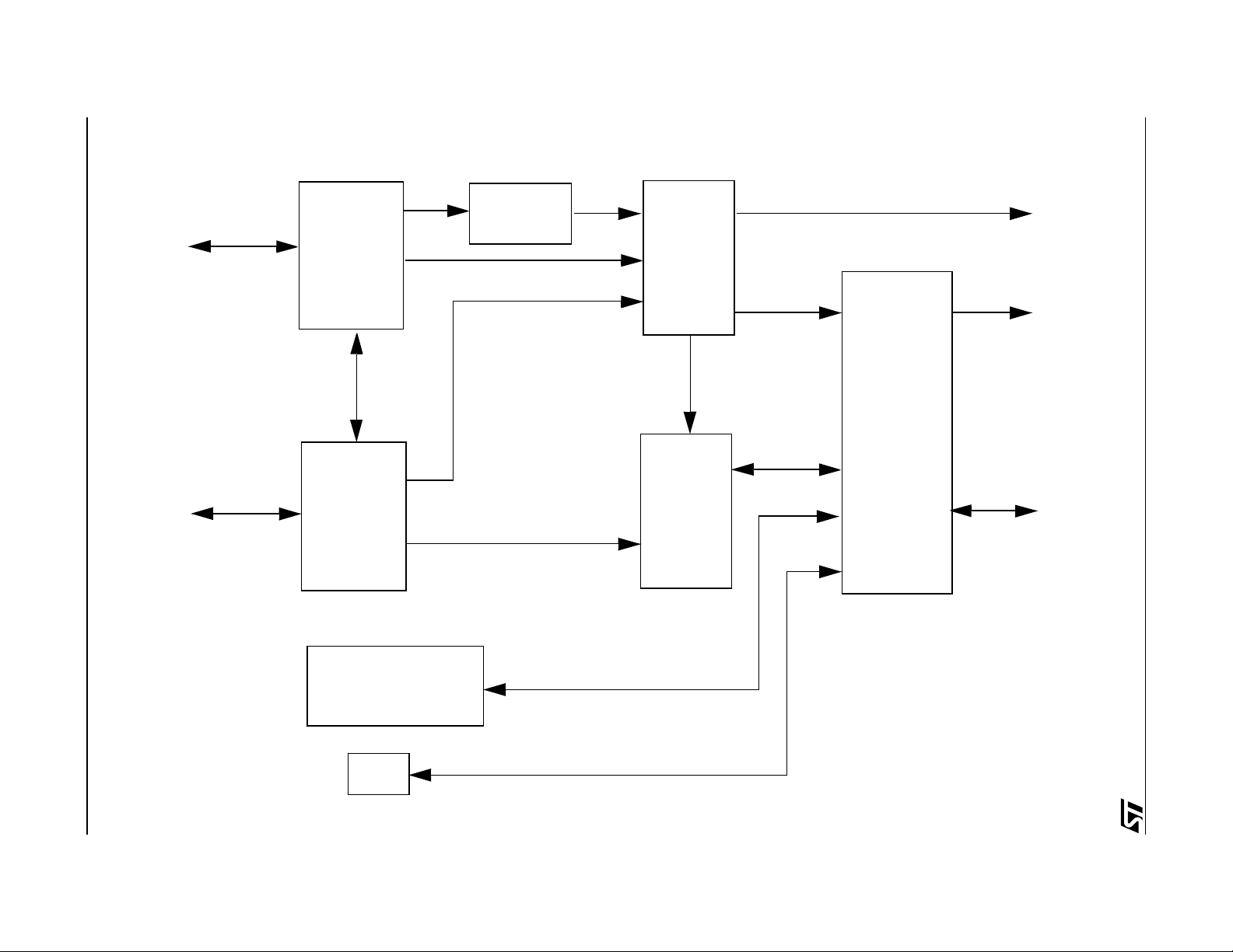
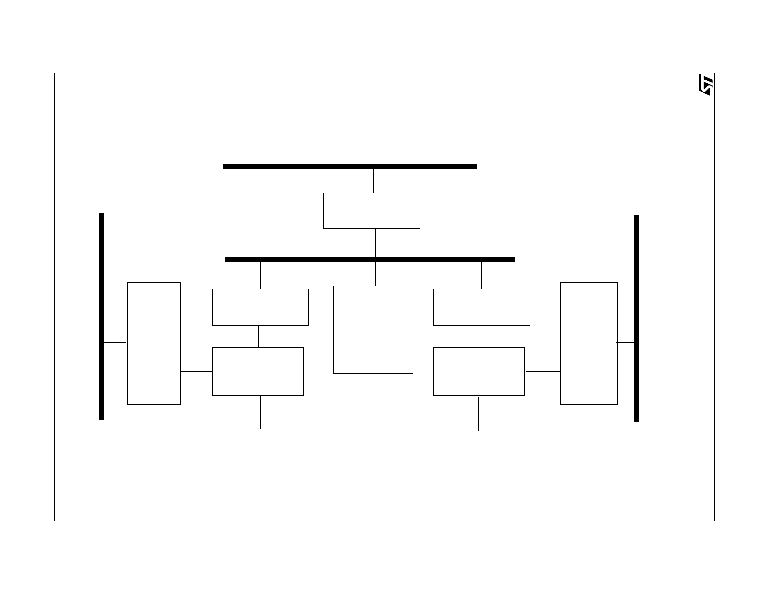
Figure 1: Block diagram
3.0 SYSTEM OVERVIEW
Three main blocks can be identified in the device architecture: ARM domain, the D950 domain and the
Clocks tree domain.
3.1 ARM7 domain
The ARM domain is a multibus microprocessor system based on the ARM7TDMI processor.
• The system bus is based on the Advanced Microcontroller Bus Architecture (AMBA) that includes
two distinct buses:
• The Advanced High performance Bus (AHB) for high performances system modules
• The Advanced Peripheral Bus (APB) for low power peripherals.
• A high speed 32 bit data bus is provided to connect external memories.
• A controller for external static memory (ESM) and a controller for external dynamic memory (EDM)
are provided.
• St atic memories, like FLASH EPROM, SRAM and dynamic memories like EDO, SDRAM, can be
2/81
Page 3

STLC1502
connected on the same external 32 bits high speed bus
• Two MII interfaces can hook directly to two 10/100 Ethernet PHYs
• Internal control hardware manages the switching and MAC processing of frames on the two Ethernet
ports
• Standard serial communication ports are available for easy device connection
• The SPI port is mainly dedicated to the CODEC control. It is compatible with the STM codecs
STLC5046, STLC5048, STW5093. It is a standard SPI port and other peripherals can be connected
to it beside the codec
• I2C port can be use to connect a LCD driver in case of IP-phone application, and a serial EEPROM
for boot coded and configuration data storage
• GPIO block includes as an alternative function a scanning key encoder for direct interface with a 6x6
keypad matrix
• Debouncing function is performed, so no overhead for the ARM controller is introduced
• UART port allows connection to a host terminal. Code downloaded through UART can be performed
during boot
• A Host Processor Interface (HPI) allows direct connection of an external control processor. The interface is directly compatible with the Motorola MPC850 external bus
3.2 D950 domain
The D950 domain is a DSP machine based on the D950 core.
• The D950 core is based on Harvard architecture with separate buses for instruction (I-bus) and data
(X-bus, Y-bus)
• The internal ROM runs basic system management code and standard vocoders
G711,G723.1A,G729AB that are included in the H.323 specification
• Additional vocoders and algorithms are downloaded from the ARM side through the DPRAM
• External CODEC is connected with a standard four wires PCM bus interface
• JT A G and emulation port are available for system software/hardware testing
• DPRAM is used as a communication channel betwee n the ARM and D950
• Control messages and voice packets are exchanged through the DPRAM
• Fax over IP support
3.3 Clock Domain
Three main clock domains are present:
• D950 and peripherals (100 MHz max)
• ARM7 and peripherals (60 MHz max)
• PCM (8.192 MHz max)
The clock base is provided by a fixed external 25MHz crystal/oscillator. A 25MHz clock output can be used
as a master clock for external Ethernet PHY devices, in 10BaseT operation.
NOTE: For 100BaseT operation, this clock may not be sufficiently stable with tight jitter requirements.
Thus the PHY’s may need their own 25 MHz crystal.
Internal PLL’s provide independent clocks to the D950 and ARM7 domain.
The ARM frequency is set by external pin, that selects between 50 MHz and 60 MHz.
The D950 frequency can be set by the ARM via Status register programming.
Four possible values are provided:
100 MHz
180 MHz
190 MHz
3/81
Page 4

STLC1502
200 MHz
To change the D950 master clock frequency the following procedure must be followed:
1) Disable the D950 clock, by resetting the DCLK bit in the control register of the MISC Control register.
2) Wait 10 ARM cycles
3) Select a new D950 master clock, by writing the MISC Status register.
4) Wait 4 ms
5) Disable the D950 clock, by setting the DCLK bit in the MISC Control register.
An Internal divider provides an internal PCM clock, 2083 KHz, that is not exactly the standard 2048 KHz.
- An external PCM clock frequency can be applied using a dedicated crystal or oscillator, to provide exactly
8KHz synch and sampling clock on the PCM bus. (External pins configuration Testsel[3:0] at [0011]).
The PCM clock rate can be selected via software to achieve the following values:
1536 (24 Ch.) 2048 (32 Ch.) 4096 (64 Ch.) 8192 KHz (128 Ch.).
- The PCM clock and Frame synch signals can be selected as inputs or outputs, by programming the con-
trol register in the miscellaneous block.
4.0 Pin Descriptions
The STLC1502 will be delivered in:
• PQFP 208 Pins
4/81
Page 5
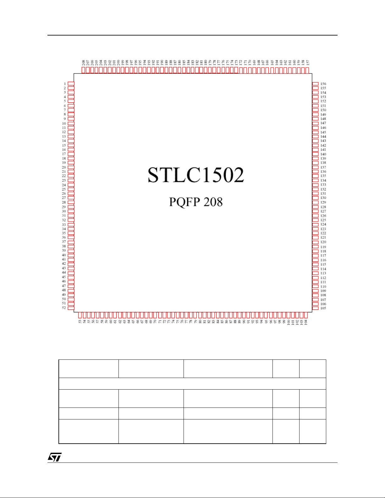
Figure 2: 208-Pin PQFP
STLC1502
4.1 Pin Description Table
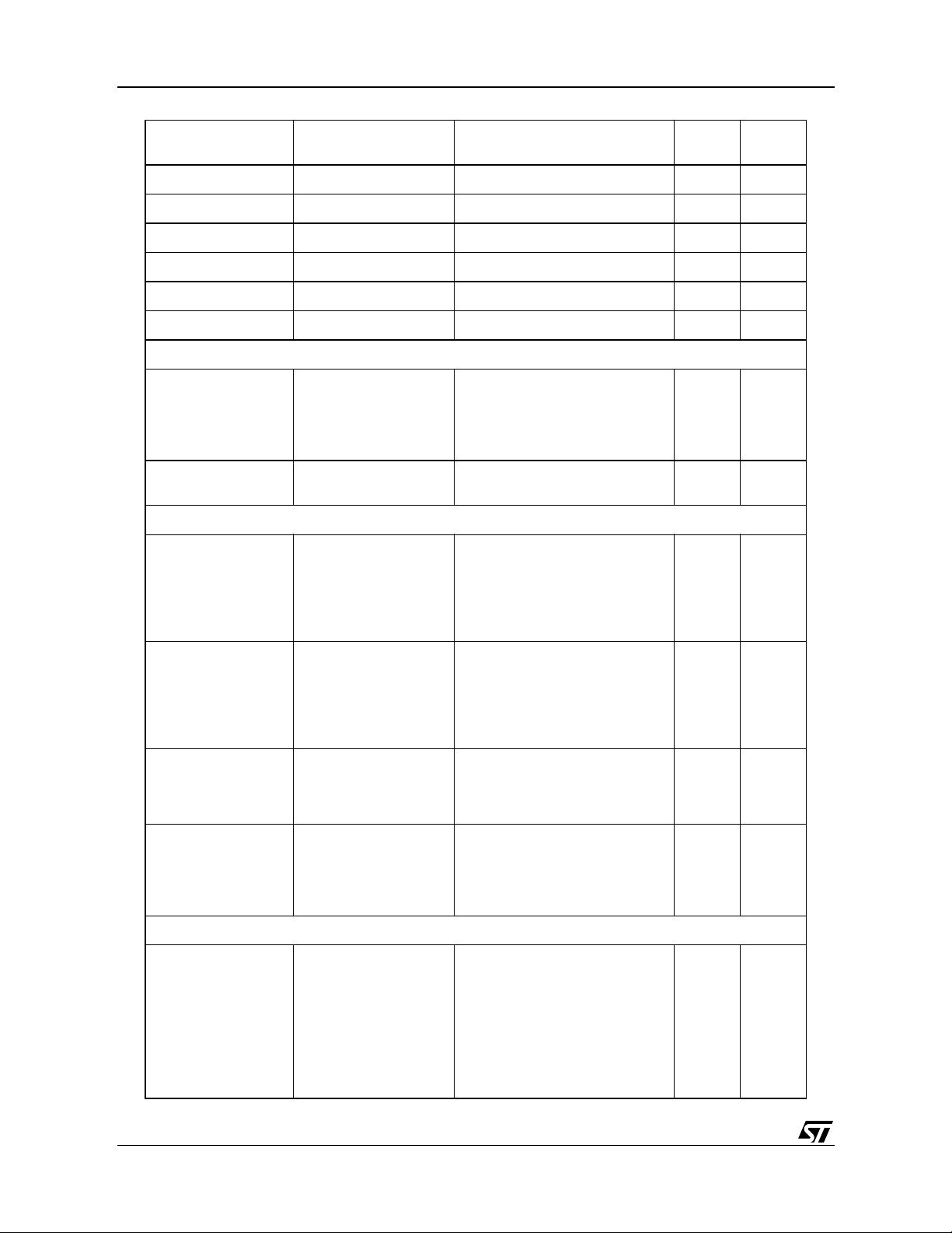
Pin Pin Name Pin Description/Note
Clocks, Reset
41 xtalin 25 MHz crystal input Master clock
42 xtalout 25 MHz crystal feedback O
43 pxtalin 8.192 MHz crystal input PCM I/F
or DSP clock in PLL bypass mode
Clock or PCM input clock in PLL
bypass mode
Pin
Drive
Pin
Type
I
I
5/81
Page 6
STLC1502
Pin Pin Name Pin Description/Note
44 pxtalout 8.192 MHz crystal feedback O
45 edmiclk SDRAM feedback clock (input) 8mA I/O
46 testarmclk ARM clock in bypass mode I
52 selarmfreq Selects ARM PII Vco frequency I
53 rstn Asynchronous Master Reset Input I
188 clkout 25MHz master clock out 4mA O
Miscellaneous
47 bootsel_treqa Boot selection: Select internal [1]
118 hp isel Select between HPI[1] or
Memory I/F (shared signals)
125, 126, 127, 129,
130, 131, 133, 134,
135, 136, 137, 138,
140, 141
add[0..13] Memory address bus.
or external [0] booting ROM. If
proper test configuration has been
selected, then signal assumes Tic
request A functionality
GPIO_KBD IF [0]
For Dynamic RAM, they are the
whole address, whereas for static,
they are the LSBits addresses. At
power up or hardware reset all
address values are 0
Pin
Drive
4mA O
Type
Pin
I
I
62, 63, 64, 65, 66, 69,
70, 71, 72, 73, 74, 75,
77, 78, 79, 81, 82, 84,
85, 86, 88, 89, 91, 92,
93, 95, 96, 98, 99,
100, 102, 103
2, 3, 4, 5 wenbsn[0..3] Write byte enable for external
6 oen Output enable for static/dynamic
ESM (specific controls)
142, 144, 145, 146,
148, 149, 150, 152
data[0..31] Memory data bus, to exchange
data between memory controller
and external memories
static RAM or byte strobe for
dynamic external RAM
external RAM. At power up or
hardware reset, the signal will be
asserted if the external booting
(bootsel = ‘1’) has been selected
add[14..21] Memory address bus’ MSBits.
They complete the ESM
addressability. A total of 4Mbyte
external (FLASH/SRAM) address
space is addressed by the
STLC1502 device. At the first fetch
of instruction after power_up or
hardware reset, all address values
are ‘0’
8mA I/O
8mA O
8mA O
4mA O
6/81
Page 7
STLC1502
Pin Pin Name Pin Description/Note
153, 154, 155 esmcs[0..2]n Chip select [0..2] for external
memory (FLASH/SR AM). At
power up or hardware reset, if
external boot ROM has been
selected, (bootsel =’1’) the signal
is asserted during the fetch
instruction, else the selection
depends on internal address
mapping
61 ecs0width External FLASH/SRAM Data bus
size: if settled to ‘L’, select a 8 bit
parallelism data.
EDM ( specific controls)
156, 158, 159, 160 edmcsn[0..3] Chip select for SDRAM or RAS for
EDO DRAM
161 edmclken SDRAM clock enable 8mA O
162 edmoclk SDRAM output clock 8mA O
165 edmras SDRAM ras command 8mA O
166 edmcas SDRAM cas command 8mA O
167 edmwe SDRAM we command 8mA O
Pin
Drive
4mA O
8mA O
Type
Pin
I
MII Interface Port # 1
168 mii1_txen Transmit enable 4mA O
169 mii1_txclk Transmit clock reference for txd,
txen, txer
170, 171, 174, 175 mii1_txd[0..3] Transmit data bus 4mA O
176 mii1_rxclk Receive clock reference for rxd,
rxdv, rxer
177 mii1_rxdv Receive data valid I
178 mii1_rxer Receive error signal, indicates an
error condition on receiving data
181, 182, 183, 184 mii1_rxd[0..3] Receive data bus I
185 mii1_col Collision signal I
186 mii1_crs Carrier sense indication I
MII Interface Port # 2
193 mii2_txclk Transmit clock reference for txd,
txen, txer
194 mii2_txen Transmit enable 4mA O
195, 196, 197, 198 mii2_txd[0..3] Transmit data bus 4mA O
I
I
I
I
7/81
Page 8
STLC1502
Pin Pin Name Pin Description/Note
200 mii2_rxclk Receive clock reference for rxd,
rxdv, rxer
201 mii2_rxdv Receive data valid I
202 mii2_rxer Receive error signal, indicates an
error condition on receiving data
203, 204, 205, 206 mii2_rxd[0..3] Receive data bus I
207 mii2_col Collision signal I
208 mii2_crs Carrier sense indication I
PHY I/F Management
189 mdc MII management clock 4mA O
190 mdio MII management data i/o 4mA I/O
UART I/F
112 sin Serial data input I
113 sout Serial data output 2mA O
I2C I/F
Pin
Drive
Pin
Type
I
I
116 scl I2C clock 2mA I/O
117 sda I2C data 2mA I/O
PCM I/F
104 pdx PCM Downstream data I
105 pdr PCM Upstream data 2mA O
106 pfs PCM Input/Output Frame
107 pdc PCM Input/Output Data clock 4mA I/O
SPI I/F
109 sck SPI interf ace Clock 2mA O
110 smi SPI master data input I
111 smo SPI master data output 2mA O
KBD/GPIO/HPI I/F
9 gpio0_r1_hpidata0 GPIO[0] or keypad matrix row 1 or
10 gpio1_r2_hpidata1 GPIO[1] or keypad matrix row 2 or
synchronization
2mA I/O
4mA I/O
Hpidata[0]
4mA I/O
Hpidata[1]
8/81
1 1 gpio2_r3_hpidata2 GPIO[2] or keypad matrix row 3 or
Hpidata[2]
4mA I/O
Page 9

STLC1502
Pin Pin Name Pin Description/Note
14 gpio3_r4_hpidata3 GPIO[3] or keypad matrix row 4 or
Hpidata[3]
15 gpio4_r5_hpidata4 GPIO[4] or keypad matrix row 5 or
Hpidata[4]
16 gpio5_r6_hpidata5 GPIO[5] or keypad matrix row 6 or
Hpidata[5]
17 gpio6_c1_hpidata6 GPIO[6] or keypad matrix col 1 or
Hpidata[6]
18 gpio7_c2_hpidata7 GPIO[7] or keypad matrix col 2 or
Hpidata[7]
19 gpio8_c3_hpiadr0 GPIO[8] or keypad matrix col 3 or
Hpiadr[0]
20 gpio9_c4_hpiadr1 GPIO[9] or keypad matrix col 4 or
Hpiadr[1]
23 gpio10_c5_hpiadr2 GPIO[10] or keypad matrix col 5 or
Hpiadr[2]
24 gpio11_c6_hpiclk GPIO[11] or keypad matrix col 6 or
Hpiclk input
Pin
Drive
4mA I/O
4mA I/O
4mA I/O
2mA I/O
2mA I/O
2mA I/O
2mA I/O
2mA I/O
2mA I/O
Pin
Type
25 gpio12_dreq GPIO[12] or Dma input request
(software selection)
26 gpio13_dack GPIO[13] or Dma output
acknowledge (software selection)
27 gpio14_hpics_d950idle GPIO[14] or Hpi Chip Select
(active low) or D950 emulator
output idle state
28 gpio15_hpias_d950snap GPIO[15] or Hpi Address Strobe
(active low) or D950 snap output
sate
29 gpio16_hpirw_treqb GPIO[16] or Hpi Read (active
high) Write (active low) strobe or
Tic request B input. The Tic mode
is forced selecting the proper test
configuration through testsel[3..0]
pin
30 gpio17_hpiint_tack GPIO[17] or Hpi Interrupt out or
Tic acknowledge output. The Tic
mode is forced selecting the
proper test configuration through
testsel[3..0] pin
33 gpio18_irq1 GPIO[18] and External interrupt
input 1
2mA I/O
2mA I/O
2mA I/O
2mA I/O
2mA I/O
2mA I/O
2mA I/O
9/81
Page 10
STLC1502
Pin Pin Name Pin Description/Note
34 gpio19_irq2 GPIO[19] and External interrupt
input 2
Test Signal
55, 56, 57, 58 testsel[0..3] Test mode selection I
Stradivarius STLC1502 and/or ARM’s JTAG
119 tdi Data input I
120 tdo Data output 2mA O
121 tms Test mode select I
122 tck Clock I
123 trstn Jtag Input Reset I
D950’s JTAG
35 d950tdi Data input I
36 d950tdo Data output 2mA O
37 d950tms TMS command I
38 d950tck Clock I
Pin
Drive
2mA I/O
Pin
Type
39 d950trstn Reset Input I
D950’s EMU signals
54 d950erqn Halt request to enter emulation
Power and Ground pins
1, 12, 21, 31, 67, 76,
83, 90, 97, 124, 132,
139, 147, 164, 180,
192, 199
7, 13, 22, 32, 40, 51,
60, 68, 80, 87, 94,
101, 108, 115, 128,
143, 151, 157, 163,
173, 179, 191
8, 48, 59, 114, 172,
187
49 PLL_VSS PLL digital ground P
50 PLL_VDD PLL analog power supply 2.5V P
vdd3 I/O Power P
gnd Core ground P
vdd Core Power P
5.0 ARM Memory Configuration
I
mode
• The AMBA bus system allows to handle memory blocks and peripherals on distinct buses, in order to
optimize the AHB architecture for maximum speed .
10/81
Page 11

STLC1502
• The memory blocks are attached to the AHB bus so ARM code can run at maximum speed.
• An internal ROM is used to store boot code that polls serial peripherals (I2C EEPROM, UART) and
HPI for code download in external RAM. After download, the control is given to code in external
RAM.
• An internal RAM is used to store ARM7 interrupt vectors and some data (network frames)
• Four external memory types can be connected.
• Flash
• SRAM
• DRAM (SDRAM or EDO)
• Serial EEPROM
• Flash, SRAM, DRAM share the same 32 bits data bus and 32 bits address bus. Little/Big endian
mode is software programmable for the DRAM memory controller. Serial EEPROM can be connected to the I2C bus.
• The chip provides the option of booting from Flash or from serial EEPROM, by selection from an
external BOOT_SEL pin. So different memory configuration s are possible depending on the application:
1. Flash, DRAM: The boot code including BOO TP and TFT P is stored in Flash. Application can be
stored in flash also, or can be downloaded into DRAM from Ethernet Network or UART.
2. EEPROM, DRAM: The boot is perf ormed from inte r n a l ROM. The ROM code loads th e code stored
in EPROM that includ es BOO TP and TFTP. Applic at ion code w ill be downl oaded int o D RA M from
Ethernet or UART .
3. Flash, DRAM, EEPROM: It is like case 1, but has more flexibility. The EEPROM can be used to store
Network parameter data (MAC address) and other specific board data, so the code to store in flash is
the same for all the platforms, and you do not need to split the flash in a permanent storage area and
in an upgradable storage area. The EEPROM can also be used to allow the programming of the flash
the first time with a code downloaded from Ethernet Network.
4. DRAM: The boot is performed from internal ROM. The application code is downloaded from the host
processor through the HPI interface. To access external memory bus an internal decoder is implemented, that can select different external memory devices. 32 bits data bus is provided with the possibility to select external accesses at 16 and 8 bits for each memory bank. For example the flash can
be at 16 bits and the DRAM at 32 bits. There are 3 chip select available for static memory (4Mbytes
each), 4 chip selects for dynamic memory (8Mbytes each).
5.1 ARM Memory Map
The ARM microprocessor sees 5 main memory areas.
Actually the memory map depends on the phase the microprocessor is working on:
• Boot from internal ROM phase (REMAP=0 and BOOT_SEL=0);
• Boot from external Flash phase (REMAP=0 and BOOT_S E L=1);
• Operating phase (REMAP=1).
The first two phases are alternative (only one of them happens at the power on reset, while the third happens
after the boot.
6.0 AHB Bus
AHB Bus is a 32 bits data and 32 bits address bus.
6.1 Internal RAM
An internal Static RAM 2048x 32 is mapped starting at address 0x0 in operational mode and is used for ARM
interrupt vector tables.
11/81
Page 12
STLC1502
6.2 ESM interface
• The ESM (External Static Memory) interface is used to access static RAMs or Flash devices. It provides 3 chip select signals and gives external access to 21 address bits, so that the memory space
accessible through each chip select is 4 Mbytes.
• The data bus on ESM external interface is 32bits wide, with the additional ability to perform 16 and 8
bits accesses. Little endian byte ordering is used. The data bus and address bus pins are shared with
the DRAM driver, using EBI interface.
• Programmable per chip-select wait-states from 0 to 15 internal clock cycles are available.
• At reset, every CS space has 15 wait states. The actual value is contained in the downloaded code.
• The external memory spaces are mapped by the ESM interface as reported in Figure 4.
• There are 3 addressable memory spaces 0x00400000 byte long each.
04000000
ESM_CS0
043FFFFF
04400000
ESM_CS1
04000000
ESM
External
Memories
ESM_CS2
047FFFFF
04800000
04BFFFFF
04C00000
07FFFFFF
Reserved
07FFFFFF
Figure 4: ESM memory map
Following is the list of the available external signals that implement SRAM or F LASH read and write cycles. Data
and address buses are not shown as they are shared with the DRAM EBI interface.
NAME Signal type Description
ESM_CS(2:0) OUT Chip Select. Asserted when the
ESM decodes the proper address
space in order to select the right
external device
OE
OUT
Output Enable. Asserted during a
read cycle (shared with EDM)
12/81
Page 13
NAME Signal type Description
STLC1502
WE[3:0]
OUT
Bytes Write enable. They are
used to select one/two bytes
when a x16/x32 Flash/SRAM is
present (shared with EDM).
0: lower byte
1: 2nd byte
2: 3rd byte
3: higher byte
ESM_CS0WIDTH
IN
This input informs whether a x8
(ESM_CS0WIDTH=0) or x16
(ESM_CS0WIDTH=1) device is
present on the CS0. This information is needed the boot from external memory is selected.
A[21:0] OUT 22 Address lines for up to
4Mbytes address space (shared
with EDM A[13:0])
D[31:0]
A scheme of the ESM control interface is reported in Figure 5.
device side
INOUT Data bus(shared with EDM bus)
external side
ESM_CS(2:0)
OE
WE[3:0]
ESM_CS0WIDTH
Figure 5: ESM control interface
Every CS space can be programmed through internal register (one for each CS) in order to:
• select the number of wait states to perform external access depending on the speed of the external
device mapped on that memory area
• select if the data bus is x8 or x16 (available only for CS1 to CS2). When the x8 memories are used,
their data bus has to be placed on the ESM_D(7:0) signals
The wait states number f or the ext ernal memories (dependi ng on memory access t ime) is obt ained from the
software code during the download phase. During the initialization phase, it is the responsibility of the software
to determine if a SRAM or a FLASH is present or not on a given CS space and the width of CS1-2 memories (if
13/81
Page 14
STLC1502
present).
It is possible to connect every CSx to a Dual Port SRAM and use that as a communication mailbox betwee n the
device and an external microprocessor. For example, the microprocessor can write a message in the memory
using one port and can send an interrupt to the dev i ce so t hat t he executi on routi ne rel ated wit h that i nterrupt
can read from the other port of the memory connected to the same CSx of the ESM.
Viceversa, the ESM can write a message in the memory and then can send an interrupt to the external microprocessor t hat will r ead the message from the other port of the memory.
The SRAM and the FLASH dev ices that are used as references are standard.
6.2.1 ESM address decoding scheme
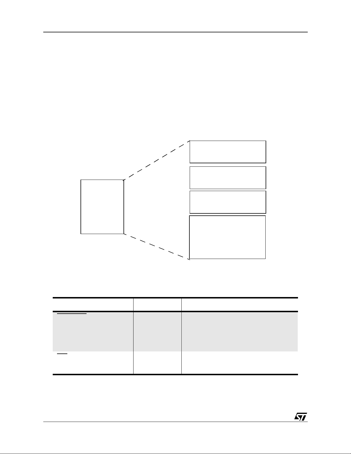
The ESM block includes also a decoder in order to generate the proper CS to the external device. In particular
this decoder will wor k on the b it 22,2 3,24 and 25 of the internal ARM address bus.
ESM decoder ESM_A(21:0)
ESM decoding scheme
6.2.2 ESM Register Map [
The base address of the ESM register is 0x0C600000.
0x0C600000
]
Address Register
R/W Notes
Name
ESMBase + 0x00 CS0 R/W CS0 bank control
ESMBase + 0x04 CS1 R/W CS1 bank control
ESMBase + 0x08 CS2 R/W CS2 bank control
6.3 EDM interface
The EDM interface is used to access external DRAMs. This block supports both EDO and SDRAM interfaces
with enough flexibility to be used with several DRAM chips available in the market. This block has a separate
bus for control (the registers are placed on the APB bus) and for data (data and address are placed on the ASB
bus) and also includes an external bus interface that allows to share address and data bus pins with the static
ESM interface.
Figure 6 shows a block diagram of the EDM block.
14/81
Page 15
15/81
STLC1502
APB
bus
AHB
bus
Registers
AHB
interface
Refresh
Memory
driver
Data
Mux
Control
Address
External
bus
interface
Data
ESM
External Static
Memory Co ntroller
TIC
Page 16
STLC1502
Figure 6: EDM block diagram
It is possible to connect up to 4 external chips with x8, x16, and x32 data bus. Each memory bank space is
8Mbytes big so that a standard 64Mbi t DRAM device can be connected. It is not possible to use a single
32Mbytes memory device.
It is the responsibility of the ARM c ode to properly configure the EDM block to initialize the DRAM at startup.
The external memory is mapped by the EDM interface as shown in Fig. 7.
10000000
EDM_CS0
107FFFFF
10000000
13FFFFFF
EDM
External
DRAM
EDM_CS1
EDM_CS2
EDM_CS3
10800000
10FFFFFF
11000000
117FFFFF
11800000
11FFFFFF
12000000
Reserved
13FFFFFF
Figure 7: EDM memory map
In the following table there is the list of the available external signals of the EDM interface.
NAME Signal type Description
EDM_CS(3:0) OUT Chip Select. Asserted when the EDM
decodes the proper address space in order
to select the right external device. To be connected to RAS signal in case of use of EDO
memorie s
EDM_CLK OUT
EDM_CLKEN
16/81
OUT
SDRAM Memory clock (same as ARM
clock). Not used with EDO.
SDRAM clock enable. Not used with EDO.
Page 17
NAME Signal type Description
STLC1502
EDM_RAS
EDM_CAS
OEN
OUT
OUT
OUT
SDRAM RAS signal. Not used with EDO.
SDRAM CAS signal. Not used with EDO
SRAM Output Enable. Not used with
SDRAM
EDM_WE
OUT
DRAM Write Enable
EDM_BS(3:0) OUT SDRAM byte strobe. CA S w hen EDO memo-
ries are used
EDM_A(21::0) OUT DRAM address lines, only 14 lines are
driven.. Lines.21:14 are driven by static
memory cont ro l le r
EDM_D(31:0) INOUT DRAM data lines, shared with static memory
controller lines.
The EDM block includes a decoder in order to generate proper CS to the external device. In particular this decoder will work on bits 25 and 26 of internal ARM address bus.
EDM
Decoder
EDM decoding scheme
• Every CS space can be programmed through internal register in order to configure the EDM to work
with the proper external device
• The DRAM Controller has nine registers, the configuration register, four bank registers and four
SDRAM configuration registers. The registers are accesses via the APB bus. The register data path
is 16 bits wide.
6.3.1 EDM Register Ma p [0x0C5800 00]
• The base address of the EDM register is 0x0C580000
Address Register
Name
EDMBase +
0x00
EDMBase +
0x04
MB1Config
MB2Config
R/W Notes
R/W
R/W
Memory Bank 1 Configuration Register
Memory Bank 2 Configuration Register
EDM_A(13:0)
17/81
Page 18
STLC1502
Address Register
Name
EDMBase +
0x08
EDMBase +
0x0C
EDMBase +
0x10
EDMBase +
0x14
EDMBase +
0x18
EDMBase +
0x1C
EDMBase +
0x20
MB3Config
MB4Config
SDRAM1C
onfigLo
SDRAM1C
onfigHi
SDRAM2C
onfigLo
SDRAM2C
onfigHi
SDRAM3C
onfigLo
R/W Notes
R/W
R/W
WO
Memory Bank 3 Configuration Register
Memory Bank 4 Configuration Register
Memory Bank 1 Low SDRAM Configuration Register
WO
Memory Bank 1 High SDRAM Configuration Register
WO
Memory Bank 2 Low SDRAM Configuration Register
WO
Memory Bank 2 High SDRAM Configuration Register
WO
Memory Bank 3 Low SDRAM Configuration Register
EDMBase +
0x24
EDMBase +
0x28
EDMBase +
0x2C
EDMBase +
0x30
6.3.1.1 Memory Bank Configuration registers
Memory bank configuration registers are used to setup memory bank specific parameters:
1514131211109876543210
Reserved DEVWID DATA-
SDRAM3C
onfigHi
SDRAM4C
onfigLo
SDRAM4C
onfigHi
MemConfig
WO
WO
WO
R/W
LAT
Memory Bank 3 High SDRAM Configuration Register
Memory Bank 4Low SDRAM Configuration Register
Memory Bank 4 High SDRAM Configuration Register
Memory Configuration Register
SETUP TIME IDLET IME SDRAM-
COL
DEVWID: Device Width
18/81
Page 19

STLC1502
• Defines the data width of the external memory device:
• 00 - Byte (8 bit)
• 01 - Half Word (16 bit)
• 10 - Word (32 bit)
DATALAT: Data Latency
• Defines the number of memory clock cycles between the start of a memory read access and the first
valid data.
• The DATALAT value is valid between 0 and 3.
SETUPTIME: Setup Time
• Defines the number of memory clock cycles t he m emory driver spends in the DECODE state before
accessing the external memory.
• The SETUPTIME value is valid between 0 and 7.
IDLETIME: Idle Time
• Defines the minimum time the memory driver must spend in the IDLE state following memory
accesses.
• The value defines the number of Memory Clock cycles.
• The IDLETIME value is valid between 0 and 7.
SDRAMCOL : SD RAM Column Width Definition
• Specifies the width of the SDRAM column address:
• 00 - 8 bits
• 01 - 9 bits
• 10 - 10 bits
• 1 1 - reserved
6.3.1.2 SDRAM Configuration registers
These registers are write only. A write access to the high registers will start the SDRAM configuration cycle,
during which the value written to the register will be asserted on the memory bus for a one clock period.
Low SDRAM Configuration Registers
1514131211109876543210
Reserved MIAB
MIAB: Memory Interface Address Bus
High SDRAM Configuration Registers
15 14 13 12 11 10 9 8 7 6 5 4 3 2 1 0
Reserved MIVE MIAA MISA
19/81
Page 20
STLC1502
MIAB: Memory Interface Address Bus
MIWE: Memory Interface Write Enable
MIAA: M e mory Interface Access A ctive (nCAS)
MISA: M e mory Interface Setup Active (nRAS)
After the power-up the CPU must configure each SDRAM device, i.e. perform precharge-refresh-mode register
set procedure.
6.3.1.3 Memory Configuration register
Memory configuration registers are used to setup parameters that are same for all banks:
15 14 13 12 11 10 9 8 7 6 5 4 3 2 1 0
Reserved PWS TYPE B3EN B2EN B1EN B0E N R EFR
PWS: Power save mode
• If PWS bit is set to’1’, the next refresh cycle will set the memory devices in the self-refresh mode.
• The memories will exit the self-refresh mode, when the PWS mode is set to’0’.
TYPE: M e mory type:
• The TYPE bit is used to select a type of the external memory.
•1 - SDRAM
•0 - EDO
B3EN: Bank 3 enable
B2EN: Bank 2 enable
B1EN: Bank 1 enable
B0EN: Bank 0 enable
• The bank enable bits are used to enable each bank separately.
• If an AHB transfer is accessing a disabled bank, the DRAM Controller will return the error response
to the AHB master.
REFR: Refresh period
• The REFR value is used to determine the refresh period. The period can be set in the 1 us steps.
• REFR Refresh Period
• 00000000 Refresh is disabled
• 00000001 Refresh period is 1us
• 00000010 Refresh period is 2us
•.
• 11111111 Refresh period is 255us
6.4 DMA Controller
• The DMA controller is intended to be used with the Ethernet switch block to transfer Ethernet frames
between the Ethernet switch buffers and memory.
• The DMAC needs initialization before starting operation. During operation it does not need interven-
20/81
Page 21

STLC1502
tion from the ARM controller.
• In receive, when the complete frame is stored in memory, the DMAC asserts the interrupt for the
ARM that can read the frame.
• In transmit the DMAC provides an interrupt when the complete frame is transferred.
6.5 Ethernet Switch
The Ethernet switch block interfaces two MAC cores to implement a 3-port Ethernet Fast switch and MAC layer
for the Embedded VoIP network software.
Main features of the block are:
• Internal FIFOs for easy DMA transfers.
• Full duplex support using separate Tx, Rx FIFOs.
• Fast switching using hardware connections between the two MAC cores. ARM microcontroller is not
involved in the switching function.
• Support for priority mechanism for voice packets, using store-and-forward procedure for incoming
data packets.
• VLAN support
• 10/100 Mb/s data transfer rates
• The MAC cores provide 2 MII interfaces to connect two external PHYs.
The device works normally as a bidirectional switch between the two ports. When the following conditions happen the device triggers additional operations:
• Received frame destination MAC address matches device MAC address. The frame is transferred to
memory using DMA, and is not switched to the other port.
• A frame has to be transmitted by the device. In this case the block waits for the end of the current
frame being switched if any. If the frame is a voice frame, as soon as the line is free the block starts
transfer of the frame. Eventual incoming frames in the same direction are stored and forwarded after
the voice frame has been sent.
The block diagram of the Ethernet switch is shown below:
21/81
Page 22
AHB bus
APB bus
Config
Control
registers
Internal bus
DMA_MAC
MAC
MII1
Bridge/arbiter
Ethernet
switching
memory
DMA_MAC
MAC
MII2
APB bus
Config
Control
registers
STLC1502
22/81
Page 23
STLC1502
6.5.1 The DMA Descriptors Chain
The Descriptor list is the mean the CPU and the DMA_MAC use to communicate each other in order to
transmit/receive frames on the cable. This list must be properly prepared before initiating any transfer
activity to/from the cable. The Descriptor is produced by the CPU and consumed by the DMA_MAC.
DMA_Cntl
DMA_Addr
DMA_Next
Tx/Rx_Status
Descr 1
(4 X 4 Bytes)
Frame 0
DMA_Cntl
DMA_Addr
DMA_Next
Tx/Rx_S tatus
Descr 2
(4 X 4 Bytes) (4 X 4 Bytes)
Frame 1
. . .
DMA_Cntl
DMA_Addr
DMA_Next
Tx/Rx_S t at us
Descr n
Frame n
• A Descriptor is a 16-bytes element which provides the DMA_MAC with information about how to
transmit/receive a single frame and how to report the transfer status back to the CPU.
• A Descriptor can be stored in any main memory location with a 32-bit aligned address.
• The first 3 words stored in a Descriptor are expected to be the values of the 3 DMA_MAC registers
describing a DMA transfer (DMA_Cntl, DMA_Addr and DMA_Next). When the DMA_MAC fetches a
Descriptor it loads this three values into its own corresponding registers.
• The last word is to be used by the DMA_MAC to report the transfer status.
6.5.2 The Descriptor control bits
The Descriptor keeps information about a single frame transfer and how to access t he next Descriptor.
The following discussion is rela ted to 3 bits of the Descriptor: the VALID bit, the NXT_EN bit and the
NPOL_EN bit.
The Descriptor can be accessed simultaneously by the CPU and the DMA_MAC. This concurrent access
is synchronized by the VALID bit in the DM A_Cntl register. When the VALID bit is equal to 0 then the
CPU is the owner of the Des criptor. Otherwise the owner is the DMA _M AC. Since t he Des criptor can be
accessed in write mode by the owner only at any time, race conditions are guaranteed to never happen.
The NXT_EN bit enables the fetch of the Next Descriptor. When the DMA_MAC finds this bit set to 0 then
its activity is considered to be completed as soon a s the current descriptor DMA transfers have been
compl eted .
The NPOL_EN bit enables the DMA_MAC to keep polling for a non-valid Descriptor until its VALID bit is
set to one. When the DMA_MAC finds both the NPOL_EN bit and the VALID bit set to 0 then its activity is
considered to be completed.
23/81
Page 24

STLC1502
6.5.3 Transfer interrupts
The DMA_MAC can interrupt the CPU with three different levels of information about transfer completion.
The CPU can choose which interrupt needs to be enabled. The y do not exclud e each ot her though; they
can be all three enabled at the same time.
The TX_CURR_DONE (RX_CURR_ DONE) interrupt bit reports the CPU when a single Descriptor (i.e.
one frame) has been completely treated by the DMA_MAC and the CPU is agai n the owner (VALID bit
set to 0).
The TX_NEXT (RX_NEXT) in terrupt bit is set when next descriptor fetch is e nabled (NXT_EN=1 in the
current descriptor) the next Descriptor is not valid (V ALID bit is off).
The TX_DONE (RX_DONE) interrupt bit is set when a whole DMA transfer is complete. This can happen
either when the current is the last Des criptor i n t he chain (NXT_EN is off) or when the next Descriptor is
not valid yet (VALID bit is off) and the polling is disabled (NPOL_EN bit is off).
6.5.4 Frames transmission (TX)
When the CPU wants to t ransm it a set of frames on t he cable, it needs to p rovide t he DMA_M A C wi th a
Descriptor list. The CP U is expec t ed to allocat e a D es cript or for each f rame it wants to s end, to fill i t with
the DMA control information and the pointer to the frame, and to link the Descriptor in the chain. The
frames will be sent on the cable in the same order they are found in the chain.
6.5.6 Open list approach
The simplest way to construct a Descriptor chain is the open list approach. Every Descriptor but the last
one will have the DMA_Next field pointing to the next Descriptor in the chain, the NXT_EN bit and the
VALID bit on, the NPOL_EN bit on /off. The last Descriptor will be set in the same way e xcept for the
NXT_EN bit (off) and the DMA_Next field (NULL).
• The CPU starts the DMA activity loading the physical location of the first Descriptor into the DMA
Next register of the DMA_MAC and set the DMA Start register enable bit to on.
• The DMA_MAC will then keep fetching the Descriptors one by one until it finds the NXT_EN bit of the
last Descriptor set to off. Every time it completes a Descriptor (f rame) it saves the t ransfer stat us i nto
TxRx_Status, it turns the Descriptor VALID bit to off and raises the TX_CURR_DONE interrupt bit.
• When the NXT_EN bit is found to be off, that means the DMA_MAC has fetched the last Descriptor in
the chain. When it completes also this Descriptor (the end of the DMA transfer) it raises both the
TX_CURR_DONE and the TX_DONE interrupt bits.
6.5.7 Closed list approach
The approach above is easy since it doesn’t require the DMA_MAC and the CPU to synchronize their access to the Descriptor chain. The problem is that it requires the CPU to build the list every time it needs a
transfer.
A faster way to operate is building a closed Descriptor list only the first time and using the VALID bit to
mark the end of the transfe r. The polling facility could also be used to s ave the CPU from the activity of
programming the DMA Start register every time it needs to start the DMA transfer. Instead, the DMA Start
register will be activated only once and the DM A_MAC will keep poll ing the invalid descript or, raising
each time the TX_NEXT interrupt bit (if enabled), until the CPU finally sets its VALID bit to on. Since the
DMA transfer practically never ends, note that in this case the TX_DONE interrupt bit is never raised.
24/81
Page 25
STLC1502
With this approach every Descriptor will have the DMA_Next field pointing to the next Des criptor in the
chain (the last on e w ill po int to the first on e) , the NX T_EN bit, the VALID bit and the N PO L _E N bit on.
The DMA_MAC will keep fetching the Descriptors one by one until it finds one with its VALI D bit set to of f.
Every time the DMA_MAC completes a Descriptor (frame) it saves the transfer status into TxRx_Status,
it turns its VALID bit to off and raises the TX_CURR_DONE interrupt bit.
6.5.8 Frames reception (RX)
The frame reception process is somethin g that needs to be activated at the be ginning and kept always
running. For this reason the closed Descriptor list (see above) is much more useful than the open list
approach.
Again, with this approach every Descriptor will have the DMA_Next field pointing to the next Descriptor in
the chain (the last one will point to the first one), the NXT_EN bit, the VALID bit and the NPOL_EN bit on.
The CPU starts the transfer activity loading the DMA Next register of the DMA_MAC with the physical
location of the first Desc riptor and set the DMA Start register enable bit to o n.The DMA_MAC wi ll start
fetching the Descriptors one by one, driven by the frames reception from the line. Every time the
DMA_MAC completes a Descriptor (frame) it saves the transfer status into TxRx_Status, it turns its
VALID bit to off and raises the TX_CURR_DONE interrupt bit.
Eventually, the DMA_MAC will be faster than the CPU, it will wrap around the Descriptor chain and find a
Descriptor still invalid.
Then the DMA_CNT keeps polling the invalid descriptor, raising each time the TX_NE XT interrupt bit (if
enabled), until some Descriptor gets available (note that in this case some frame could be lost). In the
meantime the CPU should consume the frames received and set the VALID bit to on of all the Descriptor
released.
As soon as the DM A _CNT finds the Descript or v alid agai n, i t w ill be abl e t o co m plete t he t rans fer and t o
fetch the next Descriptor.
6.5.9 Ethernet block Register Map [0x0C680000]
The base address of the Ethernet registers is 0x0C680000
The memory map of the Dual MAC Ethernet block is shown below:
Address Register Name Notes
DMA_MAC1 Eth_base1=0x0C680000
Eth_base1+ 0x0000 DMA_ST&CNTL DMA Status and Control Register
Eth_base1+0004 DMA_INT_EN DMA Interrupt Sources Enable R egister
Eth_base1+0008 DMA_INT_STAT DMA Inter rupt Status Register
Eth_base1+000C Reserved
Eth_base1+ 0x0010 RX_DMA_START RX DMA start Register
25/81
Page 26

STLC1502
Address Register Name Notes
Eth_base1+ 0x0014 RXD_DMA_CNTL RX Data DMA Control Register
Eth_base1+ 0x0018 RXD_DMA_ADDR RX Data DMA Base Address Register
Eth_base1+ 0x001C RXD_DMA_NXT RX Data DMA Next Descriptor Address
Register
Eth_base1+ 0x0020 RX_DMA_CADDR RX DMA Current Address R egister
Eth_base1+ 0x0024 RX_DMA_CXFER RX DMA Current Transfer Count Regis-
ter
Eth_base1+ 0x0028 RX_DMA_TO RX DMA FIFO Time Out Register
Eth_base1+ 0x002C RX_DMA FIFO RX DMA FIFO Status Register
Eth_base1+ 0x0030 RXV_DMA_CNTL
RX Voice DMA Control Register
Eth_base1+ 0x0034 RXV_DMA_ADDR RX Voice DMA Base Address Register
Eth_base1+ 0x0038 RXV_DMA_NXT RX Voice DMA Next Descriptor Address
Register
Eth_base1+0x003C-
Reserved
Eth_base1+0x 004C
Eth_base1+ 0x0050 TX_DMA_START TX DMA start Register
Eth_base1+ 0x0054 TXD_DMA_CNTL TX Data DMA Control Register
Eth_base1+ 0x0058 TXD_DMA_ADDR TX Data DMA Base Address Register
Eth_base1+ 0x005C TXD_DMA_NXT TX D a ta DMA N e xt Descriptor Address
Register
Eth_base1+ 0x0060 TX_DMA_CADDR TX DMA Current Address Register
Eth_base1+ 0x0064 TX_DMA_CXFER TX DMA Current Transfer Count Regis-
ter
Eth_base1+ 0x0068 TX_DMA_TO TX DMA FIFO Time Out Register
Eth_base1+ 0x006C TX_DMA FIFO TX DMA FIFO Status Register
Eth_base1+ 0x0070 TXV_DMA_CNTL TX Voice DMA Control Register
Eth_base1+ 0x0074
26/81
TXV_DMA_AD DR TX Voice DMA Base Address Register
Page 27

STLC1502
Address Register Name Notes
Eth_base1+ 0x0078 TXV_DMA_NXT TX Voice DMA Next Descriptor Address
Register
Eth_base1+0x007C-
Reserved
Eth_base1+ 0x00FC
Eth_base1+ 0x0100 RX_FIFO_0 R X FIFO 32 bit word #0
.... ... ...
Eth_base1+ 0x013C RX_FIFO_15 RX FIFO 32 bit word #15
Eth_base1+ 0x0180-
Reserved
Eth_base1+ 0x01FC
Eth_base1+ 0x0200 TX_FIFO_0 T X FIFO 32 bit word #0
.... ... ...
Eth_base1+ 0x023C TX_FIFO_15 TX FIFO 32 bit word #15
Eth_base1+ 0x0280-
Reserved
Eth_base1+ 0x03FF
Eth_base+ 0x0400-
MAC110
Eth_base+ 0x07FF
DMA_MAC2 Eth_base2 = 0x0C680800
Eth_base2+ 0x000 DMA_ST&CNTL DMA Status and Control Register
Eth_base2+0x0004 D MA_INT_EN DMA Interrupt Sources Enable Register
Eth_base2+0x8008 DMA_INT_STAT DMA Interrupt Status Register
Eth_base2+0x000C Reserved
Eth_base2+ 0x0010 RX_DMA_START RX DMA start Register
Eth_base2+ 0x0014 RXD_DMA_CNTL RX Data DMA Control Register
Eth_base2+ 0x0018 RXD_DMA_ADDR RX Data DMA Base Address Register
Eth_base2+ 0x001C RXD_DMA_NXT RX Data DMA Next Descriptor Address
Register
Eth_base2+ 0x0020 RX_DMA_CADDR RX DMA Current Address R egister
27/81
Page 28

STLC1502
Address Register Name Notes
Eth_base2+ 0x0024 RX_DMA_CXFER RX DMA Current Transfer Count Regis-
ter
Eth_base2+ 0x0028 RX_DMA_TO RX DMA FIFO Time Out Register
Eth_base2+ 0x002C RX_DMA FIFO RX DMA FIFO Status Register
Eth_base2+ 0x0030 RXV_DMA_CNTL
RX Voice DMA Control Register
Eth_base2+ 0x0034 RXV_DMA_ADDR RX Voice DMA Base Address Register
Eth_base2+ 0x0038 RXV_DMA_NXT RX Voice DMA Next Descriptor Address
Register
Eth_base2+0x003C-
Reserved
Eth_base2+004C
Eth_base2+ 0x0050 TX_DMA_START TX DMA start Register
Eth_base2+ 0x0054 TXD_DMA_CNTL TX Data DMA Control Register
Eth_base2+ 0x0058 TXD_DMA_ADDR TX Data DMA Base Address Register
Eth_base2+ 0x005C TXD_DMA_NXT TX D a ta DMA N e xt Descriptor Address
Register
Eth_base2+ 0x0060 TX_DMA_CADDR TX DMA Current Address Register
Eth_base2+ 0x0064 TX_DMA_CXFER TX DMA Current Transfer Count Regis-
ter
Eth_base2+ 0x0068 TX_DMA_TO TX DMA FIFO Time Out Register
Eth_base2+ 0x006C TX_DMA FIFO TX DMA FIFO Status Register
Eth_base2+ 0x0070 TXV_DMA_CNTL TX Voice DMA Control Register
Eth_base2+ 0x0074
TXV_DMA_AD DR TX Voice DMA Base Address Register
Eth_base2+ 0x0078 TXV_DMA_NXT TX Voice DMA Next Descriptor Address
Register
Eth_base2+0x007C-
Reserved
Eth_base2+ 0x00FC
Eth_base2+ 0x0100 RX_FIFO_0 R X FIFO 32 bit word #0
.... ... ...
28/81
Page 29

Address Register Name Notes
Eth_base2+ 0x013C RX_FIFO_15 RX FIFO 32 bit word #15
STLC1502
Eth_base2+ 0x0180-
Reserved
Eth_base2+ 0x01FC
Eth_base2+ 0x0200 TX_FIFO_0 T X FIFO 32 bit word #0
.... ... ...
Eth_base2+ 0x023C TX_FIFO_15 TX FIFO 32 bit word #15
Eth_base2+ 0x0280-
Reserved
Eth_base2+ 0x03FF
Eth_base2+ 0x0400Eth_base2+ 0x07FF
6.6 Arbiter
The arbiter is used to ensure that, at any point in time, only one master has access to the bus. It performs this
function by observing all of the bus master requests to use the bus, and deciding which is currently the highest
priority. It has a standard interface to all bus masters and split-capable slaves in the system. However it does
not support SPLIT bus transfers.
A bus m aster m ay reques t the bus during any cycl e by setti ng its HB USRE Q output HIGH . Thi s is th en sam pled
by the arbiter on the rising edge of the clock, and passed through the priority algorithm to decide which master
will have access to the bus during the next cycle. The HGRANT then outputs change to indicate which master
currently is granted control of the bus.
The HLOCK signals may be used to ensure that during an indivisible transfer, the current grant outputs do not
change. HLOCK must be asserted at least one cycle before the l ocked transfer to prevent t he arbiter from
changing the grant signals. When more than one master requests ownership of the system bus , the priority used
for arbitration is:
• Highest: TIC
• Printer Drive Control
• DMA Controller
• Lowest: ARM7TDMI (default master)
The ARM7TDMI will periodically assume top priority on the system bus: this period can be programmed. Also,
it will assume top priority when an interrupt occurs, if the interrupt mode is enabled. During reset, and when no
other masters are requesting control of the bus, the ARM7TDMI is selected as the currently granted master.
This minimizes the delay required for the core to perform a transfer on the bus, as it does not have to wait to be
granted control of the bus before it can start a new transfer.
The system also requires a default master, which is selected when no masters are granted control of the bus,
for example, when all system bus masters are waiting for split transfers to complete. The default master performs IDLE transfers while it is granted control of the bus. The bus grant output s may change while HREADY
is LOW, but the newly granted master may only drive the bus when the current tr ansfer has completed. This
requires that bus masters only drive the bus after they detect that both their HGRANT and HREADY inputs are
set HIGH.
All registers used in the system are clocke d from the rising edge of the system clock HCLK, and use the asynchronous reset HRESETn. The arbiter control and status registers are accessed via the APB bus.
MAC110 Refer to the InSilicon MAC110 specifica-
tion (see Ref. [2])
29/81
Page 30

STLC1502
6.7 TIC-Test Interface Controller
The Test Interface Controller (TIC) is a state machine that provides an A M B A AHB bus master for system test.
It reads test write and address data from the external data bus TESTBUS (XD), and uses the External Bus Interface (part of the DRAM Controller) to drive the external bus with test read data, allowing the use of only one
set of outpu t tr istate b uffers onto TESTBUS .
The TIC is used to convert externally applied t est vect ors into internal transf ers on t he AHB bus. A three-wire
external handshake protocol is used, with t wo inputs c ontroll ing t he ty pe of v ect or that i s appl ied and a single
output that indicates when the next vector can be applied. Typicall y the TIC is the highest pri ority AMBA bus
master, which ensures test access under a ll conditions. The TIC model supports address incrementing and control vectors. This means that the address for burst transfers can automatically be generated by the TIC.
6.8 AHB-ASB bridge
The APB bridge is the only bus master on the Advanced Peripheral Bus. In fact, the APB bridge is also a slave
on the AHB. The bridge unit converts ASB transfers into APB transfers. On the APB bus only 16 bits wide data
accesses are permitted. 32 bit wide and 8 bit wide transfers are not supported. All the APB peripherals decodes
all the 16 bits of the PA bus.
APB decoder space PA(15:0)
APB decoding scheme
Every area is 128k x 16 bits but the area actually available is 32k x 16 due to the fact that the address lines on
the APB bus are 16 (PA(15:0)). That means that in every area dedicated to the several block on the APB bus
only the first FFFF is usable.
7.0 APB bus
The APB bus is a 16 bits data and 16 bi ts address bus. The blocks attached on this bus are described in the
following sections while the memory area is reported in the following figure.
All the addresses in the APB space are word aligned (addresses are multiples of four)
30/81
Page 31

Figure 8: APB Mem ory Map
0C000000
Timer
0C07FFFF
STLC1502
Miscellaneous I/O
Interrupt Controller
Dual Port SRAM
Reserved
SPI port
I2C port
UART
GPIO
0C080000
0COFFFFF
0C100000
0C17FFFF
0C180000
0C1FFFFF
0C200000
0C27FFFF
0C280000
0C2FFFFF
0C300000
0C37FFFF
0C380000
0C3FFFFF
0C400000
0C47FFFF
HPI
Watchdog Timer
EDM regs
ESM regs
Ethernet Mac DMACs
DMAC
ARM/D950 bridge
0C480000
0C4FFFFF
0C500000
0C57FFFF
0C580000
0C5FFFFF
0C600000
0C67FFFF
0C680000
0C6FFFFF
0C700000
0C7FFFFF
0C800000
0C8FFFFF
31/81
Page 32

STLC1502
7.1 Timer
The Timer module connects to the Advanced Peripheral Bus.
CKTIMER
To PIC
To EDM
PWRITE
PENABLE
BnRES
DSEL_TIMER
PA[15:0]
PRDAT A [15:0]
PWDATA [15:0]
INTCT1
INTCT2
INTCT3
INTCT4
Prescaler
Load Registers
Control Registers
Control Logic
Control Section
FRC - Free Ru nning
counter
FRC - Free Ru nning
counter
Timer Section
Figure 9: Timer block diagram
This implementation consists of two major sections comprising:
• All the control logic
• Two instantiations of the free-running counters (FRCs)
The timer module has a series of memory-mapped locations that allow the state of the timer module to be read
from and written to via the APB.
7.1.1 Timer introduction
Two timers are defined and can be selected by the Control register:
• Free-running mode:The timer wraps after reaching its zero value, and continues to count down from
the maximum value.
• Periodic timer mode:The counter generates an interrupt at a constant interval.
7.1.2 Timer operation
The timer is loaded by writing to the load register and, if enabled, counts down to zero. When zero is reached,
an interrupt is generated. The interrupt may be cleared by writing to the Clear register.
After reaching a zero count, if the timer is operating in free-running mode it continues to decrement from its maximum value. If periodic timer mode is selected, the timer reloads from the load register and continues to decrement. In this mode the timer effectively generates a periodi c interrupt. The mode is selected by a bit in the
Control register.
At any point, the current timer value may be read from the Value register.
The timer is enabled by a bit in the control register. A t reset , t he timer is di sabled, the i nt errupt i s cleared and
the Load register is undefined. The mode and prescale values are also undefined.
32/81
Page 33

Load Control
Load Register Control Register
STLC1502
Timer
16-bit Down Counter
Terminal Count
Clock
Value
Figure 10: Timer block diagram
The timer clock is generated by a prescale unit. The timer clock may be one of:
• The CKTIMER
• The CKTIMER divided by 16, generated by 4 bits of prescale
• the CKTIMER divided by 256, generated by a total of 8 bits of prescale
CKTIMER
Divide
by 16
Divide
by 16
Interrupt
Timer
Clock
Prescale
Select
Figure 11: Pre-scaler bloc k diagram
Using the recommended 2.208Mhz clock, the minimum interval between two timer interrupt is 452nsec (corresponding to the 2.208Mhz period) while the maximum interval between two timer interrupt is around 6sec.
7.1.3 Timer register map [0x0C000000]
The base address of the timer register is 0x0C000000
33/81
Page 34

STLC1502
The offset of any particular register from the base address is the following.
Address Register Name R/W Notes
TimerBase + 0x00 Timer1Load R/W Timer1Load. The Load register
contains the initial value of the timer
and is also used as the reload
value in periodic timer mode.
TimerBase + 0x04 Timer1Value R Timer1Value. The Value location
gives the current value of the timer.
TimerBase + 0x08 Timer1Control R/W Timer1Control. The Control regis-
ter provides enable/disable, mode
and prescale configurations for the
timer (see Figure 10).
TimerBase + 0x0C T imer1Clear W Timer1Clear. Writing to the Clear
location clears an interrupt generated by the counter timer.
TimerBase + 0x10 Timer2Load R/W Timer2Load. The Load register
contains the initial value of the timer
and is also used as the reload
value in periodic timer mode.
TimerBase + 0x14 Timer2Value R Timer2Value. The Value location
gives the current value of the timer.
TimerBase + 0x18 Timer2Control R/W Timer2Control. The Control regis-
ter provides enable/disable, mode
and prescale configurations for the
timer (see Figure 10).
TimerBase + 0x1C T imer2Clear W Timer2Clear. Writing to the Clear
location clears an interrupt generated by the counter timer.
TimerBase + 0x20 Timer3Load R/W Timer3Load. The Load register
contains the initial value of the timer
and is also used as the reload
value in periodic timer mode.
TimerBase + 0x24 Timer3Value R Timer3Value. The Value location
gives the current value of the timer.
34/81
Page 35

STLC1502
Address Register Name R/W Notes
TimerBase + 0x28 Timer3Control R/W Timer3Control. The Control regis-
ter provides enable/disable, mode
and prescale configurations for the
timer (see Figure 10).
TimerBase + 0x0C T imer3Clear W Timer3Clear. Writing to the Clear
location clears an interrupt generated by the counter timer.
TimerBase + 0x30 Timer4Load R/W Timer4Load. The Load register
contains the initial value of the timer
and is also used as the reload
value in periodic timer mode.
TimerBase + 0x34 Timer4Value R Timer4Value. The Value location
gives the current value of the timer.
TimerBase + 0x38 Timer4Control R/W Timer4Control. The Control regis-
ter provides enable/disable, mode
and prescale configurations for the
timer (see Figure 10).
TimerBase + 0x3C T imer4Clear W Timer4Clear. Writing to the Clear
location clears an interrupt generated by the counter timer.
7.2 Watchdog Timer
STLC1502 contains a Watchdog timer. This timer is used to reset the ARM7 in case of a software deadlock.
The watchdog timer generates a hot reset when it overflows which will restart the ARM, but the code wi ll
not be downloaded again. The timer should be cleared by the software before it overflows.
It is based on a 8 bit counter which is clocked by a slow signal coming from a 17 bit prescaler clocked by
the system clock.
So the elapsing time of the watchdog timer depend on the system clock:
SYS_CLK:
13MHz => 2.58 seconds
26MHz => 1.29 seconds
39MHz => 0.86 seconds
52MHz => 0.64 seconds
This peripheral consists of a timer that continue to run and to reset the core if the software doesn’ t clear
it before it elapses. The software can clear or disable the timer by writing the WDOG_CONTROL register
7.2.1 Watch Dog Register Map [0x0C500000]
35/81
Page 36

STLC1502
The base address of the WDT register is 0x0C500000
The memory map of the WDT peripheral is shown below:
Address Register Name R/W Notes
ESMBase + 0x00 WDTControl R/W WDT cont rol register
ESMBase + 0x04 WDT reset_stat R/W WDT reset the status register
ESMBase + 0x08 WDT max_count R/W WDT programmable max count
ESMBase + 0x0C WDT counter R WDT internal counter value
7.3 Miscellaneous I/O
All the registers not related to any module attac hed to the APB/AHB bus such as EII, Test are considered M iscellaneous I/O. Additionally, the ESM configuration register and the Dual Port register are also part of this block.
7.3.1 Miscellaneous Register Map [0x0C080 000]
The Miscellaneous register address is
0x0C080000
Address Register Name R/W Notes
MISC_regBase+ 0x00 Contr ol W This register allows to control the
reset/boot procedure and some
other control features
MISC_regBase+ 0x10 Status W This register allows DSP section
setting
MISC_regBase+ 0x20 IDENTIFICATION R This register provides informa-
tions about the device/system
7.4 Interrupt Controller
In an ARM system, two levels of interrupt are available:
• FIQ (Fast Interrupt Request) for fast, low latency interrupt handling
• IRQ (Interrupt Request) for more general interrupts
Ideally, in an ARM system, only a single FIQ source would be in use at any particular time. This provides a true
low-latency interrupt, because a single source ensures that the interrupt service routine may be executed directly without the need to determine the source of the interrupt. It also reduces the int errupt latency because the
extra banked registers, which are available for FIQ interrupts, may be used to maximum efficiency by preventing
the need for a context save.
Separate interrupt controllers are used for FIQ and IRQ.
There are 15 interrupt causes available in the IRQ controller coming from:
• Software (internally generated)
•Timer1
36/81
Page 37

STLC1502
•Timer2
•UART
• Dual Port RAM
•I2C
• Ethernet switch DMAC1
• Ethernet switch DMAC2
• SPI
•DMAC
•IRQ1/GPIO18
•IRQ2/GPIO19
•IKybd
•HPI
•Timer3
Even if only a single bit position is defined for FIQ, the interrupt controller can drive one of the interrupt source
(IRQ interrupt sources), through a register, in order to generate the FIQ interrupt.
The IRQ interrupt controller uses a bit position for each different interrupt source.
All interrupt source inputs must be active HIGH and level sensitive and it remain active until the interrupt cause
has been cancelled.
No hardware priority scheme nor any form of interrupt vectoring is provided, because thes e functions can be
provided in software.
A programmed interrupt register is also provided to generate an interrupt under software control.
Every interrupt source can be masked.
7.4.1 Interrupt control
The IRQ interrupt management is done as described in the following:
• An interrupt is generated by a given device/source;
• This cause is readable by the IRQRawStatus register;
• If not masked (the mask is set by IRQEnableSet and reset by IRQEnableClear), this interrupt will
generate a IRQ signal to the ARM and the interrupt source will be known by a read of the IRQStatus
register.
• The ARM will serve the IRQ reading at first in the IRQStatus the active interrupt requests and will
execute with a given priority the proper interrupt routine. Every routine must erase (quite soon) in
some way its interrupt request source. This causes also for the proper bit in the IRQRawStatus register and in the IRQStatus register to disappear.
The same interlock is present for the FIQ interrupt.
7.4.2 Interrupt control scheme
37/81
Page 38

STLC1502
BCLK
PWRITE
PENABLE
BnRES
DSEL_INT
PA[15:0]
PRDATA [15:0]
PWDATA [15:0]
Figure 11: Interrupt block schem e
FIQ
Control
NFIQ
NFIQ
NIRQ
IRQSource[13:0]
IRQ
NIRQ
Control
38/81
Page 39

INTERRUPT_MASK
STLC1502
Enable
IRQRawStatus
Interru p t Source
Other Interrupt Bit Slices
Figure 12: IRQ control block
7.4.3 Interrupt register map [0x0C100000]
The base address of the timer register is
The offset of any particular register from the base address is the following.
Address Register Name R/W Notes
0x0C100000
IRQStatus
Interrupt Pending
nIRQ
Int.Base + 0x00 IRQStatus R For every IRQ interrupt cause,
a ‘1’ means an active pending
interrupt that has to be served
by the ARM
Int Base+ 0x04 IRQRaw Status R For every IRQ interrupt source,
a ‘1’ means an active pending
interrupt “before” the mask (w/
o considering the mask)
Int.Base + 0x08 IRQEnabl eSet R/W Fo r every IRQ interrupt source,
a ‘0’ means that even if an
interrupt source is active, it has
to be stopped (masked). The
write operation of 1 to a given
bit, enable the corresponding
interrupt
39/81
Page 40

STLC1502
Address Register Name R/W Notes
Int.Base + 0x0C IRQSoft R/W Only the bit 1 ha s to be used.
Writing ‘1’ it generates an interrupt mapped in the bit 1 of the
IRQStatus and of the IRQRa wStatus registers. Writing ‘0’ the
software interrupt cause is
erased.
Int.Base + 0x10 FIQStatus R For the FIQ interrupt cause, ‘1’
means an active pending interrupt that has to be served by
the ARM.
Int Base + 0x14 FIQRawStatus R Fo r the IRQ interrupt source, a
‘1’ means an active pending
interrupt “before” the mask (w/
o considering the mask)
Int.Base + 0x18 FIQEnableSet R/W For the FIQ interrupt source, a
‘0’ means that even if an interrupt source is active, it has to
be stopped (masked). The
write operation of 1 to the bit0,
enables the interrupt
Int.Base + 0x1C IRQEnableClear W The write operation of 1 to a
given bit, disables the corresponding interrupt. As consequence, the corresponding bit
in the IRQEnableSet goes to 0
(interrupt disabled).
Int.Base + 0x20 FIQEnableClear W The write operation of 1 into
the bit 0 disables FIQ interrupt
cause. As a result, the bit 0 in
the FIQEnableSet goes to 0
(interrupt disabled).
Int.Base + 0x24 IRQTestSource R/W Usable wh en the bit 0 of the
IRQSourceSel is set to one. In
this case this register is the
interrupt source cause. If set,
the cause is active (interrupt
generated) while if reset, the
cause is not active.
40/81
Page 41

STLC1502
Address Register Name R/W Notes
Int Base + 0x28 IRQSourceSel R/W Select the test mode of the IRQ
cause on the interrupt controller (if the bit 0 is set). In this
case the IRQTestSource
becomes the interrupt source
cause.
Int.Base + 0x2C FIQTestSource R/W Usable when the bit 0 of the
FIQSourceSel is set to one. In
this case this register is the
interrupt source cause. If set,
the cause is active (interrupt
generated) while if reset, the
cause is not active.
Int Base + 0x30 FIQSourceSel R/W Select the test mode of the FIQ
cause on the interrupt controller (if the bit 0 is set). In this
case the FIQTestSource
becomes the interrupt source
cause. Moreover this register
contains also the selection for
the FIQ interrupt cause.
7.5 SPI-Serial Peripher al Interface
The Serial Peripheral Interface (SPI) allows full-duplex, synchronous, serial communication with external
devices. An SPI system may consist of a mas ter and one or more slaves or a system in which devices
may be either masters or slaves.
The SPI is normally used for communication between the microcontroller and external peripherals.
7.5.1 Main Features
• Full duplex, three-wire synchronous transfers
• Master mode operation (clock generation)
• Four master mode frequencies
• Four programmable master bit rates
• Programmable clock polarity and phase
• End of transfer interrupt flag
• Write collision flag protection
• Master mode fault protection capability.
The SPI is connected to external devices through 3 pins:
SMI: Master In
SMO: Master Out
SCK: Serial Clock p in
41/81
Page 42

STLC1502
When the master device transmits data to a slave device via SMO pin, the slave device responds by sending data to the master device to the SMI. This implies full duplex transmission with both data out and data
in synchronized with the same clock signal (which is provided by the master device via the SCK pin).
Thus, the byte transmitted is replaced by the byte received and eliminates the need for separate transmitempty and receiver-full bits. A status flag is used to indicate that the I/O operation is complete.
The MSB is transmitted first.
Four possible data/clock timing relationships may be chosen.
7.5.2 Programming procedure
The SPI interface contains 3 dedicated registers:
• A Control Register (CR)
• A Status Register (SR)
• A Data Register (DR)
Check the register description section for bits position and functions.
Select the SPR0 & SPR1 bits to define the serial clock baud rate.
Select the CPOL and CPHA bits to define one of the four relationships between the data transfer and the
serial clock.
The transmit sequence begins when a byte is written in the DR register. The data byte is parallely loaded
into the 8-bit shift register (from the internal bus) du ring a write cycle and then shifted out serially to the
SMO pin most significant bit first. When data transfer is complete:
The SPIF bit is set by hardware
.An interrupt is generated if the SPIE bit is set and the I bit in the CCR register is cleared.
During the last clock cycle the SPIF bit is set, a copy of the data byte received in the shift register
is moved to a buffer. When the DR register is read, the SPI peripheral returns this buffered value.
Clearing the SPIF bit is performed by the following software sequence:
1. An access to the SR register while the SPIF bit is set
2. A read to the DR register.
Note: While the SPIF bit is set, all writes to the DR register are inhibited until the SR register is read.
7.5.3 Data Transfer Format
During an SPI transfer, data is simultaneously transmitted (shifted out serially) and received (shifted in serially). The serial clock is used to synchronize the data transfer during a sequence of eight clock pulses.
Four possible timing relationships may be chosen by software, using the CPOL and CPHA bits.
The CPOL (clock polarity) bit controls the steady state value of the clock when no data is being transferred.
The combination between the CPOL and CPHA (clock phase) bits selects the data capture clock edge.
The master device applies data to its SMO pin before the capture clock edge.
CPHA bit is set:
The second edge on the S CK pin (f alling edge if the CPOL bit is r es et, rising edge if the CPOL bit is se t)
is the MSBit capture strobe. Data is latched on the occurrence of the second clock transition.
CPHA bit is reset
The first edge on the SCK pin (falling edge if CPOL bit is set, rising edge if CPOL bit is reset) is the MSBit
capture strobe. Data is latched on the occurrence of the first clock transition.
The slave select signal is necessary in case more than one slave devices are connected on the seral bus.
The slave select can be generated with a GPIO pin.
42/81
Page 43

STLC1502
7.5.4 Collision management
Collision is defined as a write of the DR register while the internal serial clock (SCK) is in the process of
transfer. The WCOL bi t in the S R regist er is set if a write co llision oc curs. No S PI inte rrupt is generat ed
when the WCOL bit is set (the WCOL bit is a status flag only). Clearing the WCOL bit is done through a
software sequence:
1-Read SR
2-Read DR
7.5.5 SPI register map [0x0C280000]
The base address of the Remap & Pause register is 0x0C280000.
43/81
Page 44

STLC1502
The offset of any particular register from the base address is the following.
Address Register Name R/W Notes
SPI_regBase+ 0x04 SPIDR R/W SPI Data I/O register.
SPI_regBase+ 0x08 SPICR R /W SPI configuration register
SPI_regBase+ 0x0C SPISR R/W SPI status register
7.6 I 2C bus interfa ce
The I2C Bus Interface serves as an interface between the microcontroller and the serial I2C bus. It provides both multimaster and slave functions, and controls all I2C bus-specific sequencing, protocol, arbitration and timing. It supports fast I2C mode (400kHz).
7.6.1 Main Features
• Parallel-bus/I2C protocol converter
• Multi-master capability
• 7-bit/10-bit Addressing
• Transmitter/Receiver flag
• End-of-byte transmission flag
• Transfer problem detection
I2C Master Features:
• Clock generation
• I2C bus busy flag
• Arbitration Lost Flag
• End of byte transmission flag
• Transmitter/Receiver Flag
• Start bit detection flag
• Start and Stop generation
I2C Slave Features:
• Stop bit detection
• I2C bus busy flag
• Detection of misplaced start or stop condition
• Programmable I2C Address detection
• Transfer problem detection
• End-of-byte transmission flag
• Transmitter/Receiver flag
7.6.2 General Description
In addition to receiving and transmitting data, this interface converts it from serial to parallel format and
vice versa, using either an interrupt or polled by software. The interface is connected to the I2C bus by a
data pin (SDAI) and by a clock pin (SCLI). It can be connected both with a standard I2C bus and a Fast
I2C bus. This selection is made by software.
The interface can operate in the following modes:
– Slave transmitter/receiver
– Master transmitter/receiver
44/81
Page 45

STLC1502
By default, it operates in slave mode. The interface automatically switches from slave to master after it
generates a START condition and from master to slave in case of arbitration loss or a STOP generation,
allowing then Multi-M a s ter c a pa bilit y.
In Master mode, it initiates a data transfer and generates the clock signal. A serial data transfer always
begins with a start condition and ends with a stop condition. Both start and stop conditions are generated
in master mode by software.
In Slave mode, the interface is capable of recognizing its own address (7 or 10 bits), and the General Call
address. The General Call address detection may be enabled or disabled by software.
Data and addresses are transferred as 8-bit bytes, MSB first. The first byte(s) following the start condition
contain the address (one in 7-bit mode, two in 10-bit mode). The address is always transmitted in Master
mode. A 9th clock pulse follows the 8 clock cycles of a byte transfer, during which the receiver must send
an acknowledge bit to the transmitter.
• Acknowledge may be enabled and disabled by software. The I 2 C interface address and/or general
call address can be selected by software. The speed of the I 2 C interface may be selected between
Standard (0-100KHz) and Fast I2C (100-400KHz).
• In transmitter mode the interface holds the clock in low before transmission to wait for the microcontroller to write the byte in the Data Register.
• In receiver mode: the interface holds the clock line low after reception to wait for the microcontroller
to read the byte in the Data Register.
• The SCL frequency (Fscl) is controlled by a programmable clock divider which depends on the I 2 C
bus mode.
• When the I2C cell is enabled, the SDA and SCL ports must be configured as floating inputs. In this
case, the value of the external pull-up resistor used depends on the application.
7.6.3 Functional Description
Refer to the CR, SR1 and SR2 registers in register map section for the bit definitions.
By default the I 2 C interface operates in Slave mode (M/SL bit is cleared) except when it i nitiates a t ransmit or receive sequence. First the interface frequency must be configured using the FRi bits in the OAR2
register.
7.6.3.1 Slave mode
As soon as a start condition is detected, the address is received from the SDA line and sent to the shift
register; then it is compared with the address of the interface or the General Call address (if selected by
45/81
Page 46

STLC1502
software).
Note: In 10-bit addressing mode, the comparison includes the header sequence (11110xx0) and the two
most significant bits of the address.
• Header matched (10-bit mode only): the interface generates an acknowledge pulse if the ACK bit
is set.
• Address not matched: the interface ignores it and waits for another Start condition.
• Address matched: the interface generates in sequence:
• Acknowledge pulse if the ACK bit is set.
• EVFand ADSL bits are set with an interrupt if the ITE bit is set.
Then the interface waits for a read of the SR1 register, holding the SCL line low. Next, read the DR register to
determine from the least significant bit (Data Direction Bit) if the slave must enter Receiver or Transmitter mode.
In 10-bit mode, after receiving the address sequence the slave is always in receive mode. It will enter transmit
mode on receiving a repeated Start condition followed by the header sequence with matching address bits and
the least significant bit set (11110xx1).
Slave Receiver
After the address reception and SR1 register has been read, the slave receives bytes from the SDA line
into the DR register via the internal shift register. After each byte the interface generates in sequence:
– Acknowledge pulse if the ACK bit is set
– EVF and BTF bits are set with an interrupt if the ITE bit is set.
Then the interface waits for a read of the SR1 register followed by a read of the DR register, holding the
SCL line low.
Slave Transmitter
After the address reception and the SR1 register has been read, the slave sends bytes from the DR register to the SDA line via the internal shift register. The slave waits for a read of the SR1 register followed
by a write in the DR register, holding the SCL line low.
When the acknowledge pulse is received:
– The EVF and BTF bits are set by hardware with an interrupt if the ITE bit is set.
Closing slave communication
After the last data byte is transferred a Stop Condi ti on is generated by the master. The interface detects
this condition and sets:
– EVF and STOPF bits with an interrupt if the ITE bit is set.Then the interface waits for a read of the SR2
register
Error Cases
– BERR: Detection of a Stop or a Start condition during a byte transfer. In this case, the EVF and the
BERR bits are set with an interrupt if the ITE bit is set. If it is a Stop then the interface discards the data,
released the lines and waits for another Start condition. If it is a St art then the interface discards the data
and waits for the next slave address on the bus.
– AF: Detection of a non-acknowledge bit. In this case, the EVF and AF bits are set with an interrupt if the
ITE bit is set.
Note: In both cases, SCL line is not held low; however, SDA line can remain low due to possible «0» bits
transmitted last. It is then necessary to release both lines by software.
How to release the SDA / SCL lines:
• Set and subsequently clear the STOP bit while BTF is set.
46/81
Page 47

STLC1502
• The SDA/SCL lines are released after the transfer of the current byte.
7.6.3.2 Master Mode
To switch from default Slave mode to Master mod e a Start condition generation is needed.
Start condition
Setting the START bit while the BUSY bit is cleared causes the interface to switch to M aster mode (M/SL
bit set) and generates a Start condition. Once the Start condition is sent:
– The EVF and SB bits are set by hardware with an interrupt if the ITE bit is set.
Then the master waits for a read of the SR1 register followed by a write in the DR register with the Slave
address, holding the SCL line low.
Slave address transmission
The slave address is then sent to the SDA line via the internal shift register.
In 7-bit addressing mode, one address byte is sent.
In 10-bit addressing mode, sending the first byte including the header sequence causes the following
event:
– The EVF bit is set by hardware with interrupt generation if the ITE bit is set.
Then the master waits for a read of the SR1 register followed by a write in the DR register, holding the
SCL line low. The second address byte is then sent by the interface. After completion of this transfer (and
acknowledge from the slave if the ACK bit is set):
– The EVF bit is set by hardware with interrupt generation if the ITE bit is set.
Then the master waits for a read of the SR1 register followed by a write in the CR register (for example
set PE bit), holding the SCL line low. Next the master must enter Receiver or Transmitter mode.
Note: In 10-bit addressing mode, to switch the master to Receiver mode, software must generate a
repeated Start condition and resend the header sequence with the least significant bit set (11110xx1).
Master Receiver
After the address transmission and SR1 and CR registers have been accessed, the master receives
bytes from the SDA line into the DR register via the internal shift register. After each byte the interface
generates in sequence:
– Acknowledge pulse if the ACK bit is set
– EVFand BTF bits are set by hardware with an interrupt if the ITE bit is set.
Then the interface waits for a read of the SR1 register followed by a read of the DR register, holding the
SCL line low. To close the communication: before reading the last byte from the DR register, set the
STOP bit to generate the Stop condition. The interface goes automatically back to slave mode (M/SL bit
cleared).
Note: In order to generate the non-acknowledge pulse after the last received data byte, the ACK bit must
be cleared just before reading the second last data byte.
Master Transmitter
After the address transmission and SR1 register has been read, the master sends bytes from the DR
register to the SDA line via the internal shift register. The master waits for a read of the SR1 register followed by a write in the DR register, holding the SCL line low. When the acknowledge bit is received, the
interface sets:
– EVF and BTF bits with an interrupt if the ITE bit is set.
To close the communication: after writing the last byte to the DR register, set the STOP bit to generate
the Stop condition. The interface goes automatically back to slave mode (M/S L bit cleared).
47/81
Page 48

STLC1502
Error Cases
• BERR: Detection of a Stop or a Start condition during a byte transfer. In this case, the EVF and
BERR bits are set by hardware with an interrupt if ITE is set.
• AF: Detection of a non-acknowledge bit. In this case, the EVF and AF bits are set by hardware with
an interrupt if the ITE bi t is set. To resume, set the START or STOP bit .
• ARLO: Detection of an arbitration lost condition. In this case the ARLO bit is set by hardware (with an
interrupt if the ITE bit is set and the interface goes automatically back to slave mode (the M/SL bit is
cleared).
Note: In all these cases, the SCL line is not held low; however, the SDA line can remain low due to possible «0» bits transmitted last. It is then necessary to release both lines by software.
Event Flags and interrupt genera tion diagram
7.6.4 I2C registers map [0X0C300000]
The base address of the Remap & Pause register is 0x0C300000.
The offset of any particular register from the base address is the following.
Address Register
R/W Notes
Name
I2C_regBase+ 0x20 I2CCR R/W I2C configuration register
I2C_regBase+ 0x24 I2CSR1 R/W I2C status register 1
I2C_regBase+ 0x28 I2CSR2 R/W I2C status register 2.
48/81
Page 49

STLC1502
Address Register
R/W Notes
Name
I2C_regBase+ 0x2C I2CCCR R/W I2C Clock Control register.
I2C_regBase+ 0x30 I2COAR1 R/W I2C Own Address register
I2C_regBase+ 0x34 I2COAR2 R/W I2C Own Address register
I2C_regBase+ 0x38 I2CDR R/W I2C Data I/O r egister.
7.7 UART-Universal Asynchronous Receiver Transmitter
The UART provides a serial data communication with transm it and receive channels that can operate
concurrently to handle a full-duplex operation. Two internal FIFOs for transmitted and received data,
deep 16 and wide 8 bits, are present; these FIFO s can be enabled or disabled through a registe r. Interrupts are provided to control reception and transmission of serial data.
The clock for both transmit an d receive channels is provided by an inte rnal baud rate generator that
divides its input clock by any divisor value from 1 to 2 16 - 1.
7.7.1 Operation
The UART supports full-duplex asynchronous communication, where both the transmitter and the
receiver use the same data frame format and the same baud rate. Data is transmitted on the TXD pin and
received on the RXD pin.
Data frames
8-bit data frames either consist of:
• eight data bits D0-7 (by setting the Mode bit field to 001);
• seven data bits D0-6 plus an automatically generated parity bit (by setting the Mode bit field to 01 1).
Parity may be odd or even, depending on the ParityOdd bit in the ASCControl register. An even parity bit
will be set, if the modulo-2-sum of the seven data bits is 1. An odd parity bit will be cleared in this case.
The parity error flag (ParityError) will be set if a wrong parity bit is received. The parity bit itself will be
stored in bit 7 of the ASCRx-Buffer register.
8-bit data frame
Start
bit
D0
(LSB)
D1 D2 D3 D4 D5
D6
8th
bit
1st
stop
bit
2nd
stop
bit
-Data bit (D7)
-Parit y bit
9-bit data frames either consist of:
• nine data bits D0-8 (by setting the Mode bit field to 100)
• eight data bits D0-7 plus an automatically generated parity bit (by setting the Mode bit field to 111)
• eight data bits D0-7 plus a wake-up bit (by setting the Mode bit field to 101)
49/81
Page 50

STLC1502
Parity may be odd or even, depending on the ParityOdd bit in the ASCControl register. An even parity bit
will be set, if th e mo dulo-2-su m of the eight data bits is 1. An odd parity bit w ill be c lea re d in t his cas e.
The parity error flag (ParityError) will be set if a wrong parity bit is received. The parity bit itself will be
stored in bit 8 of the ASCRx-Buffer register.
In wake-up mode, received frames are only transferred to the receive buffer register if the ninth bit (the
wake-up bit) is 1. If this bit is 0, no receive interrupt request will be activated and no data will be transferred. This feature may be used to control communication in multi-processor systems. When the master
processor wants to transmit a block of data to one of several slaves, it first sends out an address byte
which identifies the target slave. An address byte differs from a data byte in that the additional ninth bit is
a 1 for an address byte and a 0 for a dat a byte, so no s lave will be i nterrupt ed by a dat a byt e. An address
byte will interrupt all slaves (operating in 8-bit data + wake-up bit mode), so each slave can examine the
8 least significant bits (LSBs) of the received character (the address). The addressed slave will switch to
9-bit data mode, which enables it to receive the data bytes that will be coming (with the wake-up bit
cleared). The slaves that are not being addressed remain in 8-bit data + wake-up bit mode, ignoring the
following data bytes.
9-bit data frame
Start
bit
D0
(LSB)
D1 D2 D3 D4 D5
D6
D7
9th
bit
1st
stop
bit
2nd
stop
bit
- Data bit (D7)
- Parity bit
- Wake up bit
7.7.2 Baud rate generation
The UART has its own dedicated 16-bit baud rate generator with 16-bit reload capability.
The baud rate generator is clocked with the CPU clock. The timer counts downwards and can be started
or stopped by the Run bit in the ASCControl register. Each under-flow of the timer provides one clock
pulse. The timer is reloaded with the value stored in its 16-bit reload register each time it underflows. The
ASCBaudRate register is the dual-function baud rate generator/reload register. A read from this register
returns the content of the timer; writing to it updates the reload register. An auto-reload of the timer with
the content of the reload register is performed each time the ASCBaudRate register is written to. However, if the Run bit is 0 at the time the write operation to the ASCBaudRate register is performed, the
timer will not be reloaded until the first CPU clock cycle after the Run bit is 1.
The baud rate generator provides a clock at 16 times the baud rate. The baud rate and the required
reload value for a given baud rate can be determined by the following formula:
Baudrate = fCPU/(16 *ASCBaudRate)
7.7.3 The timeout interrupt
A timeout counter register provides timeout interrupt on the receive path.
Whenever the rxfifo has got something in it, the timeout counter will decrement until something happens
50/81
Page 51

STLC1502
to the rxfifo. If nothing happens, and the timeout counter reaches zero, the ASCStatus(TimeoutNotEmpty) flag will be se t. Provided ASCIntEna ble(Timeout Not Em pt y ) is set, this will cause an interrupt.
When the software has emptied the rxfifo, the timeout counter will reset and start decrementing. If no
more characters arrive, when the counter reaches zero the ASCStatus(TimeoutIdle) flag will be set. Provided the ASCIntEnable(TimeoutIdle) is set, per_interrupt will fire.
7.7.4 Interrupt control
The UART contains two registers that are used to control interrupts, the status register (ASCStatus) and
the interrupt enable register (ASCIntEnable). The status bits in the ASCStatus register determine the
cause of the interrupt. Interrupts will occur when a status bit is 1 (high) and the corresponding bit in the
ASCIntEnable register is 1.
The error interrupt signal is generated by the UART from the OR of the parity error, framing error, and
overrun error status bits after they have been ANDed with the corresponding enable bits in the ASCIntEnable register. An overall interrupt request signal (per_interrupt) is generated from the OR of the Error
Interrupt signal and the TxEmpty, TxHalfEmpty, RxHalfFull, RxBufFull signals.
Note: TxFull does not generate interrupt.
The status register cannot be written directly by software. The reset mechanism for the status register is
described below.
• TxEmpty, TxHalfEmpty are reset when a character is written to the transmitter buffer.
• TxFull is reset when a character is transmitted
• RxBufFull and OverrunError are reset when a character is read from the receive Fifo.
• The data error status bits (ParityError, FrameError) are reset when the character with error is read
from the receive Fifo.
7.7.5 UART Memory map
The base address of the UART interface is fixed by the APB bridge.
Address Register Name R/W Notes
UART_regBase+ 0x00 ASC BaudRate R/W Baud rate generator register
UART_regBase+ 0x04 ASCTxBuffer WO Transmit buffer (Fifo)
UART_regBase+ 0x08 ASCRxBuffer RO Receive buffer (Fifo).
UART_regBase+ 0x0C ASCC ontrol R/W UAR T control register.
UART_regBase+ 0x10 ASCIntEnable R/W UART interrupt enable reg-
ister
UART_regBase+ 0x14 ASCStatus RO UART status register.
UART_regBase+ 0x18 ASCGuardtime R/W UART Guartime register.
UART_regBase+ 0x1C ASCTimeout R/W UAR T Timeout register.
51/81
Page 52

STLC1502
Address Register Name R/W Notes
UART_regBase+ 0x20 ASCTxReset WO Flush Transmit buffer (Fifo)
UART_regBase+ 0x24 ASCRxReset WO Flush Receive buffer (Fifo)
7.8 GPIO/Keypad encoder
The GPIO block is available as a cell that controls 20 input/output pins. The block includes a key scanning
encoder. The encoder function is an alternative to the use of 12 I/O pins. The 12 pins are organized as a
6X6 matrix providing an interface to a 36 key keyboard. 16 pins are also multiplexed with the HPI external
interface. The HPI interface is selected by external pin HPISEL. Two pins GPIO18, GPIO19 are direct interrupt sources in the interrupt register when programmed as inputs.
The pin description of the GPIO pins can be found in the Pin Description Table in Section 4.1.
7.8.1 GPIO operation mode
The GPIO operation mode is the Parallel Port mode.
Each of the 20 signals may be programmed as an input or an output through a set up register. Once programmed, each pin maintains its identity as an input or output. Voltages are standard process port levels,
0 and 3.3 volts. The on chip ARM processor may read or write to the port at any time.
7.8.2 Keyboard operation mode
The keyboard may contain up to 36 keys. Twelve (12) port pins provide a 6x6 scanning matrix. Six of the
pins are strobes and six of the pins are inputs. The application circuitry will provide small series resistors
to prevent electrostatic damage to the port pins.
The circuitry will scan the keys at a rate of 10, 20, 40 or 80 msecs, controlled by the software. Two successive cycles are needed to validate a key. Only one key will be allowed down in a scan cycle. Once
validated as being down, the "no key down" condition must be validated for two complete cycles when the
key is released. Every valid key condition will cause the value of the key to be written to a register and
an interrupt shall be set. Two key rollover will not be supported unless the solution is easier to implement
than the method described above.
7.8.4 GPIO registers map [0x0C400000]
The base address of GPIO registers is 0x0C400000.
The offset of any particular register from the base address is the following.
Address Register
R/W Notes
Name
GPIO_regBase+ 0x00 Control R/W This register allows to set the
block functionality
GPIO_regBase+ 0x04 Mask W This r egister allows GPIO direc-
tion setting (output enable)
52/81
Page 53

STLC1502
Address Register
R/W Notes
Name
GPIO_regBase+ 0x08 Data R/W This register allows GPIO data
output setting
GPIO_regBase+ 0x0C Status R/W Key data flag
GPIO_regBase+ 0x10 Key R Key value
7.9 HPI
The HPI is dual port SRAM bas ed, with control that generates an interrupt when a message is sent. The DPRAM
is implemented on chip and has a message buffer size of 256 bytes for each direction. Input buffer is used for
messages from Host Processor to Str adivarius . Out put buf fer is used for messages f rom Stradi varius t o Host
Processor.
• The external bus interface of the HPI is compatible with Motorola MPC850 network processor. The
data bus width is 8 bits.
• A status register, an index register (for the host processor), an interrupt mask register, and a message buffer are required for both input and output transactions.
• The Input Status Register (ISR) is set by the Host Processor by writing 0x01 and cleared by writing
0x00 to the location. It is cleared by ARM by writing anything to it.
• The Output Status Registers (OSR) is set by the ARM by writing 0x01 and cleared by writing 0x00. It
is cleared by the Host Processor by writing anything to it.
• The Input and Output Index Registers (IIR & OIR respectively) are reset to their st arting value by writing 0x00 to their respective addresses. They can also be cleared by the Host Processor by writing
anything to them.
• The Input Interrupt Mask Register (IIM) resets to 0x00, causing the Mask to be set (active low). This
means that before the ARM can receive message ready interrupts from the Host Processor, this register must be written with 0x0001 (by ARM) to unmask the interrupt.
• The Output Interrupt Mask Register (OIM) resets to 0x00, causing the Mask to be set (active low).
This means that before the Host Processor can receive message ready interrupts from the ARM, this
register must be written with 0x01 (by the Host Processor) to unmask the interrupt.
• The Input and Output Message buffers are each 256 bytes long and 1 byte wide (an overflow in the
index register will not write to the other message buffer, but will start to overwrite the current message buffer).
• Addressing of the Input and Output Message Buffers by the Host Processor is implemented indirectly
via the Input and Output Index Registers. An external interrupt signal is generated when the output
status register is set by the ARM7. An ARM7 interrupt signal is generated when the input status register is set by the Host Processor.
7.9.1 Send Message from Host Processor to ARM
• Read Input Status Register. If h01, the ARM has not read out the last message. If 0x00, the ARM has
read the last message and the Input Message Buffer is available for use.
• Clear Input Index Reg by writing any value to its address (b.100).
• Write message into Input Message Buffer by consecutively writing to its address (b.111). Each write
will cause the Input Index Regist er to increm ent by 1 and access anot her byte loc ation.
• Write 0x01 to Input Status Register (address b.011) to interrupt the ARM
53/81
Page 54

STLC1502
7.9.2 Receive Message from ARM by Host Proces sor
After receiving interrupt from ARM:
• Clear Output Index Register (address b.001) by writing any value.
• Read message from Output Message Buffer by consecutively reading from its address (b.110). Each
read will cause the Output Index Register to increment by 1 and access another byte location.
• Clear the Output Status Reg (address b.000) by writing any value (the ARM can clear the OSR by
writing 0 to it).
7.9.3 Send Messag e from ARM to Host Processor
• Read Output Status Register. If h0001, the HP has not read out the last message. If 0x0000, the HP
has read the last message and the Output Message Buffer is available for use.
• Write message into Output Message Buffer. This buffer is directly addressable by the ARM.
• Write 0x0001 to Output Status Register to interrupt the HP
7.9.4 Receive Message from Host Processor by ARM
After receiving interrupt from HP:
• Read message from Input Message Buffer.This buffer is directly addressable by the ARM.
• Clear the Input Status Reg by writing 0x0001 to its address (the HP can clear the ISR by writing 0 to
it).
In the following table there is the list of the available external signals of the HPI interface.
NAME Signal type Description
HPI_CLK IN
HPI_CS
HPI_AS
IN
IN
HPI_RW IN
HPI bus clock form Host Processor
Active low select from Host Processor.
Address strobe from Host Processor.
R/W from Host Processor
HPI_ADDR(2:0) IN Host Processor address
HPI_DATA(7:0) INOUT Host Processor data bus lines.
HP_INT OUT I nterrupt to Host Processor
Table : External signals of HPI
7.9.5 HPI Memory map
54/81
Page 55

STLC1502
Table : Register map of the DPORT peripheral
Register Name ARM 7 Address Host Processor addr.
Output Status reg HPI_regBase +0x0C00 0x0
Output Index reg HPI_r egBase +0x0C02 0x1
Output Mask reg HPI_regBase +0x0C04 0x2
Input Status reg HPI_regBase +0x0C06 0x3
Input Index reg HPI_r egBase +0x0C08 0x4
Input Mask reg. HPI_regBase +0x0C0A 0x5
Output Message buffer HPI_regBase +0x0000
-
0x6
HPI_regBase +0x01FE
Output Message buffer HPI_regBase +0x0200
-
0x7
HPI_regBase +0x03FE
7.10 Dual Port SRAM
A dual port SRAM 4096x16 connected between the APB bus and the X bus of the D950 domain, is used as a
mailbox between the ARM7 and the D950. The DPRAM c an be written/read everywhere by both the ARM and
the D950. The DPRAM bank has two status sections consisting of 32, 16 bits memory locations, and a message
section consisting 4064 16 bit memory locations.
There are 4 hardware registers: ARM and D950 mailbox mask registers and ARM and D950 mailbox registers.
• Mailbox registers: the writing of any value in a STATUS location will set the corresponding bit in the
MAILBOX to 1. This will generate an interrupt if the corresponding mailbox MASK registe r bi t is set to
1, and won’t if the bit is set to 0. Reading a STATUS loc ation w ill clear th e corres ponding bit in the
MAILBOX to 0. (note: Only the ARM can clear the D950 mailbox on a read, and only the D950 can
clear the ARM mailbox on a read. Likewise only the ARM can set the ARM Mailbox bits by writing to
the ARM STATUS registers, and only the D950 can set the D950 Mailbox by writing to the D950 STATUS registers).
• Mailbox MASK registers: writing 0 in a bit location will allow the STATUS location to set the corresponding bit in the MAILBOX, but will mask out the generation of an interrupt. The Mailbox MASK
registers are both reset to all 0’s, so, by default, no interrupts will be generated.
7.10.1 DPRAM protocol
There can be up to 16 different communication channels that the D950 and the ARM can use to exchange messages between them. The allocation of the 4064 addressable message buffers locations in the DPRAM is com-
pletely under the programmer’s control. There is no intervention by the hardware on the DPR AM other than use
the first 32 locations to set and clear the MAILBOX registers and ultimately generate interrupts. A software protocol must be established in advance to safely pass messages.
Every time one of the two devices wants to write or receive a message, it should follow the example protocol
55/81
Page 56

STLC1502
here below, where the D950 sends a message to the ARM. The same apply in the reverse direction with ARM
and D950 side swapped.
• The D950 reads the D950 MAILBOX register bit corresponding to the channel it wants use for the
message. If it is set to 1, the previous message has not been read by the ARM and the channel is not
available. If the content of that bit is 0, then the D950 can write the message for the ARM into the
appropriate section of the DPRAM
• The D950 writes any value in the appropriate D950_STATUS_X location (0<= X<= 15), indicating
that the message has just been put in the DPRAM. This will cause the corresponding bit in the D950
MAILBOX register to be set to 1.
• If the corresponding bit in the D950 Mailbox Mask register is set to 1, then an interrupt request for the
ARM will be generated. The interrupt line is the logical OR of all the unmasked bits in the D950 MAILBOX register.
• The ARM interrupt service routine will read th e D950 MAI LBO X register and compare this with the
D950 Mailbox MASK register to determine which channel caused the interrupt.
• The ARM reads the appropriate section of the DPRAM. When it has finished reading the message, it
reads the corresponding D950 STATUS location.
• This latest read clears the corresponding bit in the D950 MAILBOX register. If no other unmasked
bits are set in the D950 MAILBOX register, the ARM interrupt clears, otherwise remains set.
• Multiple channels can be used concurrently . It is up to the receiver to manage this eventuality. So the
DPRAM can be used to buffer the messages as it is processed, while other channels are still available for communication.
7.10.2 Dual Port memory map [0x0C180000]
The base address of the Dual Port memory is 0x0C180000.
The base address of control registers is
The DPRAM is mapped in the ARM memory space as shown below:
0x0C188000
56/81
Page 57

DPRAM
(4096x16)
Reserved
STLC1502
0C180000
0C1803FE
0C180000
0C181FFF
DPCOMM
ARM_STATUS_0
ARM_STATUS_1
ARM_STATUS_2
ARM_STATUS_3
ARM_STATUS_ 15
D950_STATUS_0
D950_STATUS_1
D950_STATUS_2
D950_STATUS_15
Reserved
0C184000
0C184004
0C184008
0C18400C
0C18403C
0C184040
0C184044
0C184048
0C18407C
Figure 13: DPRAM memory map
4.10.2.1 DPRAM registers map
0C188000
CONTROL
REGISTERS
0C18800C
Reserved
0C181FFF
57/81
Page 58

STLC1502
Address Register Name R/W Notes
DPORT_regBase+ 0x0 D950_MAILBOX R It contains the pend-
DPORT_regBase+ 0x 4 D950_MAILB OX_MASK R/W It contains the m ask
DPORT_regBase+ 0x8 ARM_MAILBOX R It contains the pend-
ing interrupt
requests that notify
to the ARM has a
message coming
from the D950 to
read. There is an
interrupt line for
each message class
for the
D950_MAILBOX
ing interrupt
requests that notify
to the D950 has a
message coming
from the ARM to
read. There is an
interrupt line for
each message class
DPORT_regBase+
0xC
8.0 Register Map
Following is the complete list and the description of every peripheral register of the Stradivarius
Address Register Name R/W Note
0x0C000000
0x0C000004
0x0C000008
0x0C00000C
58/81
Timer1Load R/W TImer block register
Timer1Value R TImer block register
Timer1Control R/W TImer block register
Timer1Clear W TImer block register
ARM_MAILBOX_MA SK R It c ontains the mask
for the
ARM_MAILBOX
Page 59

Address Register Name R/W Note
STLC1502
0x0C000010
0x0C000014
0x0C000018
0x0C00001C
0x0C000020
0x0C000024
0x0C000028
0x0C00002C
0x0C000030
0x0C000034
0x0C000038
0x0C00003C
Timer2Load R/W TImer block register
Timer2Value R TImer block register
Timer2Control R/W TImer block register
Timer2Clear W TImer block register
Timer3Load R/W TImer block register
Timer3Value R TImer block register
Timer3Control R/W TImer block register
Timer3Clear W TImer block register
Timer4Load R/W TImer block register
Timer4Value R TImer block register
Timer4Control R/W TImer block register
Timer4Clear W TImer block register
0x0C080000 Control W Miscellaneous
0x0C080010 Status W Misce llaneous
0x0C080020 IDENTIFICATION R Miscellaneous
0x0C100000
0x0C100004
0x0C100008
0x0C10000C
0x0C100010
0x0C100014
0x0C100018
IRQStatus R Interrupt Control
IRQRawStatus R Interrupt Control
IRQEnableSet R/W Interrupt Control
IRQSoft W Interrupt Control
FIQStatus R Interrupt Control
FIQRawStatus R Interrupt Control
FIQEnableSet R/W Interrupt Control
59/81
Page 60

STLC1502
Address Register Name R/W Note
0x0C10001C
0x0C100020
0x0C100024
0x0C100028
0x0C10002C
0x0C100030
0x0C188000
0x0C188004
0x0C188008
0x0C18800C
IRQEnableClear W Interrupt Control
FIQEnableClear W Interrupt Control
IRQTestSourcet R/W Interrupt Control
IRQSourceSel R/W Interrupt Control
FIQTestSource R/W Interrupt Control
FIQSourceSel R /W Interrupt Control
D950_MAILBOX R DPORT
D950_MAILBOX_MASKR/W DPORT
ARM_MAILBOX R DPORT
ARM_MAILBOX_MASKR DPORT
0x0C280004 SPIDR R/W SPI Data I/O register.
0x0C280008 SPICR R/W SPI configuration regis-
ter
0x0C28000C SP ISR R/W SPI status register
0x0C300020 I2CCR R/W I2C c onfiguration regis-
ter
0x0C300024 I2CSR1 R/W I2C status register 1
0x0C300028 I2CSR2 R/W I2C status register 2.
0x0C30002C I2CCCR R/W I2C Clock Control reg-
ister.
0x0C300030 I2COAR1 R/W I2C Own Address reg-
ister
60/81
Page 61

STLC1502
Address Register Name R/W Note
0x0C300034 I2COAR2 R/W I2C Own Address reg-
ister
0x0C300038 I2CDR R/W I2C Data I/O register.
0x0C380000 ASCBaudRate R/W UART Baud rate regis-
ter
0x0C380004 ASCTxBuffer WO UART Transmit buffer
(Fifo)
0x0C380008 ASCRxBuffer RO UART Receive buffer
(Fifo).
0x0C38000C ASCControl R/W UART control register.
0x0C380010 ASCIntEnable R/W UART interrupt enable
register
0x0C380014 ASCStatus RO UART status register.
0x0C380018 ASCGuardtime R/W UART Guartime regis-
ter.
0x0C38001C ASCTimeout R/W UART Timeout register.
0x0C380020 ASCTxReset WO Flush Transmit buffer
(Fifo)
0x0C380024 ASCRxReset WO Flush Receive buffer
(Fifo)
0x0C480000 Control R/W GPIO/KYBD
0x0C480004 Mask W GPIO/KYBD
0x0C480008 Data R/W GPIO/KYBD
0x0C48000C Status R/W GPIO/KYBD
0x0C480010 Key R GPIO/KYBD
61/81
Page 62

STLC1502
Address Register Name R/W Note
0x0C480000 Output Status reg RO HPI output buffer status
register
0x0C480004 Output Index reg R/W HPI output buffer index
register
0x0C480008 Output Mask reg R/W HPI output interrupt
mask
0x0C48000C Input Status reg RO HPI input buffer status
register
0x0C480010 Input Index reg R/W HPI input buffer index
register
0x0C480014 Input Mask reg. R/W HPI input interrupt
mask
0x0C480800 Output Message buffer WO HPI output buffer regis-
ter
0x0C480C00 Input M essage buffer RO HPI input buffer register
0x0C500000 WDTControl R/W WDT control register
0x0C500004 WDT Reset_stat R/W WDT reset the status
register
0x0C500008 WDT Max_count R/W WDT programmable
max count
0x0C50000C WDT Counter R WDT internal counter
value
0x0C600000
MB1Config
R/W
EDM Bank 1 Configuration
0x0C600004
MB2Config
R/W
EDM Bank 2 Configuration
0x0C600008
MB3Config
R/W
EDM Bank 3 Configuration
62/81
Page 63

Address Register Name R/W Note
STLC1502
0x0C60000C
0x0C600010
0x0C600014
0x0C600018
0x0C60001C
0x0C600020
0x0C600024
0x0C600028
MB4Config
SDRAM1ConfigLo
SDRAM1ConfigHi
SDRAM2ConfigLo
SDRAM2ConfigHi
SDRAM3ConfigLo
SDRAM3ConfigHi
SDRAM4ConfigLo
R/W
WO
WO
WO
WO
WO
WO
WO
EDM Bank 4 Configuration
EDM Bank 1 Low
SDRAM
EDM Bank 1 High
SDRAM
EDM Bank 2 Low
SDRAM
EDM Bank 2 High
SDRAM
EDM Bank 3 Low
SDRAM
EDM Bank 3 High
SDRAM
EDM Bank 4 Low
SDRAM
0x0C60002C
SDRAM4ConfigHi
WO
EDM Bank 4 High
SDRAM
0x0C600030
MemConfig
R/W
EDM Configuration
Register
0x0C600000 CS0 R/W Static ESM_ CS0 bank
control
0x0C600004 CS1 R/W Static ESM_CS1 bank
control
0x0C600008 CS2 R/W Static ESM_CS2 bank
control
63/81
Page 64

STLC1502
9.0 D950 Domain
The D950 domain c onsists of a D950 core, I RAM, I RO M, X R AM, Y RAM, Tim er, Emulator, Interrupt controller
and TAP, PCM interface peripherals.
9.0 D950 memory map
The following table provides the memory map of D950 on X, Y, I buses.
Address Area name Area size
0x0000
---------
0x000F
0x0010
-------
0x001F
0x0020
-------
0x002F
0x0030
-------
0x005F
0x0060
-------
0x006F
0x0070
-------
0xFFFF
DSP registers 16 Words
EMU 16 Words
ITC 16 Words
Reserved DSP
TIM 16 Words
RAM Y 64 KWords
Mapping of D950 Y mem ory sp ace (1 Word = 16 bit)
64/81
Page 65

STLC1502
Address Area name Area size
0x0000
RAM X 32 KWords
---------
0x7FFF
0x8000
DPCOM 16 KWords
-------
0xBFFF
0xC000
PCMIF 16 KWords
-------
0xFFFF
Mapping of D950 X memory sp ace (1 Word = 16 bit)
Address Area name Area size
0x0000
---------
0x3FFF
ROM I
(first bank)
16 KWords
0x4000
-------
ROM I
(Second bank)
0x7FFF
0x8000
-------
ROM I
(Third bank)
0xBFFF
0xC000
RAM I 16 KWords
-------
0xFFFF
Mapping of D950 I memory space (1 Word = 16 bit)
9.1 DPRAM memory map [0x8000]
The base address of the DPRAM is 0x8000 in the X memory space.
16 KWords
16 KWords
65/81
Page 66

STLC1502
The base address of control registers is 0xA800 in the X memory space
For a description of DPRAM protocol refer to the DPRAM section in the ARM domain.
DPRAM
(4096x16)
Reserved
8000
8FFF
8000
BFFF
DPCOMM
ARM_STATUS_0
ARM_STATUS_1
ARM_STATUS_2
ARM_STATUS_3
ARM_STATUS _ 1 5
D950_STATUS_0
D950_STATUS_1
D950_STATUS_2
D950_STATUS_15
Reserved
A000
A001
A002
A003
A00F
A010
A011
A012
A01F
66/81
A800
CONTROL
REGISTERS
A803
Reserved
BFFF
Page 67

STLC1502
Address Register Name R/W Notes
DPORT_regBase+ 0x0 ARM_MAILBOX R It contains the pending inter-
rupt requests that notify to the
D950 has a message coming
from the ARM to read. There
is an interrupt line for each
message class
DPORT_regBase+ 0x1 ARM_MAILBOX_M
ASK
R/W It contains the mask for the
ARM_MAILBOX
DPORT_regBase+ 0x2 D950_MAILBOX R It contains the pending inter-
rupt requests that notify to the
ARM has a message coming
from the D950 to read. There
is an interrupt line for each
message class
DPORT_regBase+ 0x3 D950_MAILBOX_
MASK
10.0 PCM Interface
The PCM interface is used to actually send and receive voice samples.
On the other side, the PCM Block has an interface to the D950 Xbus.
Moreover two other signals to feed the master clock and the hardware reset are present.
R It contains the mask for the
D950_MAILBOX
67/81
Page 68

STLC1502
Figure 14: PCM-block Inte rc onnection Sch em e
XAE(15:0)
XDE(15:0)
XWREn
XRDEn
D950
PCM
DR
DX
PCLK
PFS
XBSEn
ITR3n
ITR7n
RSTn
CLK
The PCM interface has 5 main signals:
• DR (output): this is the serial data stream that the PCM sends to the codec
• DX (input): this is the serial data stream sent by the codec and received by the PCM block
• PCLK (input/output): this is the PCM clock sent to codec. In the application, the frequency is
2.048Mhz. The PCM clock can be generated by the PCM block from internal Master clock or can be
input externally, according to the bit CLKEN in configuration register
• PFS (input/output): this signal is asserted high when the frame number zero is present on the serial
data stream; it is possible to program the codec so that the PCM block asserts this signal on a given
frame (FS). The same frame number is always present in the same time on DR and DX. The PFS
can be generated by division from PCLK or can be input externally, according to FSEN in the configuration registe r.
10.1 Miscellaneous Interface
This interface has two signals:
• RSTn (input): this is the hardware active low reset
• CLK (input): this is the master input clock coming from the external os c illator at 2.048M hz in the current application.
10.2 Interrupt Event Manageme nt
There are two interrupt lines that goes to the D950.
• ITR3 line (Overrun)
• ITR7 line (Frame synch).
MISC
68/81
Page 69

PCM_INTERRUPT_MASK
STLC1502
Enable
PCM_INTERRUPT_ROW
Interrupt Source
PCM_INTERRUPT
Interrupt Pending
D950 ITR3
Other Interrupt Bit Slices
Figure 15: In te rrup t Block
10.3 Clock Distribution
• The PCM block works at 2.048Mhz clock and it is a fully synchronous design at that frequency. No
gated clock, no latches are used.
• The design is able to support also higher PCM hierarchies such as 4.096Mhz and 8.196Mhz.
• The D950 interface works as a clock stage decoupling block. It can be accessed externally at 66Mhz,
while internally it works at 2.048Mhz.
10.4 Reset Distribution and Configuration
• The PCM block has an explicit active low reset pin controlled by ARM.
• A software reset is implemented in the PCM_CONFIGURATION register at the address 0x0002.
• In the PCM_CONFIGURATION register there is also a bit that configures the FPGA itself as linear or
PCM coding.
10.5 Data Fl ow Managem ent
Per each direction the PCM block contains a double buffer used to store and forward the voi ce samples. This
has to be big enough to store all (four) voice samples coming (and going) from (to) the SLICs contained in one
PCM frame. Actually the number of bits per voice channel per PCM frame is 8 in case of PCM coding (A low or
u low) and 16 in case of linear coding. Other bits are used to provide information about the number of the logic
channel the frame is associated with.
So, it is necessary to have two memory banks per direction.
For example, in the upstream direction (from the codec to the D950), one bank is used to store the incoming
voice samples (on-line bank) and the other used to keep the voice samples received in the previous PCM frame
(off-line bank) while they are read by the D950. This mechanism is needed because the PCM flow is synchro-
69/81
Page 70

STLC1502
nous and cannot be stopped.
The memory banks are swapped between them on PCM frame basis; so while the incoming information is writ-
ten in the on-line memory, the D950 can read the information contained in the previous PCM frame from the offline memory bank. Every PCM frame (FS signal based) the on-line memory becomes off-line and viceversa.
This swap is transparent for the D950 so th at the D950 sees the tw o memory banks located always at the same
addresses.
The same scheme in a different hardware block implements the memory buffer for the downstream flow (from
the D950 to the codec).
10.6 Basic Operation
The PCM block uses the reference clock to generat e an i nternal t i me base. For example, i t generates t he FS
signal with the proper timing. Then an internal register has to store the association between the voice channel
(SLIC) and the PCM slots according to the configuration of the codec (DRA# and DXA# registers). The FS signal
is sent not only to the codec, but also to the D950 (through ITR7), in order to give it the proper timing reference.
So, between two subsequent FS signals, the D950 has to read back from the PCM block the voice samples of
the previous PCM frame and has to write i n it the P CM samples of the several v oice channels that the PCM
block itself will send to the codec in the following PCM frame.
So the ITR7 is an 8Khz interrupt signal that provides the timing reference to the D950.
10.7 PCM coding Voice Fra m e
This section describes the operation of the PCM block in case of PCM coding of the voice samples (LIN bit of
the codec CONF register set to 0x0). In this case each voice sample has 8 bits, plus 3 miscellaneous bits per
channel. So a total of 2 direction x 2 banks x 4 channels x 11 bits each (176 bits) are needed. This memory is
implemented internally in the PCM block.
The PCM_VOICE_FRAME_FROM_CODEC_x (x=0..3) and the PCM_VOICE_FRAME_TO_CODEC_x
(x=0..3) are used to store upstream and downstream voice channel x.
Selection between PCM and linear coding is done in the PCM_CONF IGURATION register
PCM Coding Upstream Basic Op eration (from the co dec to the D950)
The PCM voice samples coming from the codec are inserted in the on-line upstream memory. In the same PCM
slot, the D950 accesses at the off-line upstream memo ry through the PCM _VOICE_FRAME_FROM _CODEC_x
register connected to off-line memory. If during a PCM frame, the D950 left some unread voice data in the offline memory (in the meantime became on-line) an interrupt even is generated (OV_U bit of the
PCM_INTERRUPT register).
10.8 Linear coding Voice Frame
If the linear coding (LIN bit of the codec CONF register set to 0x1) is selected, each voice sample is coded as
a 16 bit two’s complement. This means that each voice channel takes two PCM slot to transport the voice information. For example, considering the channel x (x=0..3), for the upstream flow (voice sample from the codec to
the D950), the 8 most significant bits are transported in the PCM slot reported in the PCM_S LOT_UP field of
the PCM_SLOT_FRO M _CODE C_x register while 8 less s ignificant bits are transported in the following At reset
PCM_LIN_DATA_DO WN =0x0000.
x values: 0 ..3 .
10.9 PCM Register List
This section reports the list of the PCM block registers in the D950 domain. The address is referred to the base
address where the PCM block is placed on. In other words, they are displacement addresses. The D950 cannot
70/81
Page 71

access the ARM7 memory space.
Address Reg ister Nam e Description
STLC1502
Register List
0x0000
0x0001
0x0002
0x0003
0x0004
0x0005
0x0006
0x0007
PCM_RESET Reset Register
n/a
n/a
n/a
PCM_SLOT_FR
OM_CODEC_0
PCM_SLOT_FR
OM_CODEC_1
PCM_SLOT_FR
OM_CODEC_2
PCM_SLOT_FR
OM_CODEC_3
Upstream PCM
slot Register for
Voice Channel 0
Upstream PCM
slot Register for
Voice Channel 1
Upstream PCM
slot Register for
Voice Channel 2
Upstream PCM
slot Register for
Voice Channel 3
0x0008
0x0009
0x000A
0x000B
0x000C
PCM_SLOT_TO_
CODEC_0
PCM_SLOT_TO_
CODEC_1
PCM_SLOT_TO_
CODEC_2
PCM_SLOT_TO_
CODEC_3
PCM_INTERRUPTInterrupt
Downstream PCM
slot Register for
Voice Channel 0
Downstream PCM
slot Register for
Voice Channel 1
Downstream PCM
slot Register for
Voice Channel 2
Downstream PCM
slot Register for
Voice Channel 3
71/81
Page 72

STLC1502
Address Reg ister Name Description
0x000D
0x000E
0x000F
0x0010
0x0011
0x0012
0x0013
PCM_INTERRUP
T_MASK
PCM_INTERRUP
T_ROW
n/a
PCM_VOICE_FR
AME_FROM_CO
DEC_0
PCM_VOICE_FR
AME_FROM_CO
DEC_1
PCM_VOICE_FR
AME_FROM_CO
DEC_2
PCM_VOICE_FR
AME_FROM_CO
DEC_3
Interrupt Mask
Interrupt Row
Upstream Voice
Sample Register
for channel 0
Upstream Voice
Sample Register
for channel 1
Upstream Voice
Sample Register
for channel 2
Upstream Voice
Sample Register
for channel 3
0x0014
0x0015
0x0016
0x0017
0x0018
PCM_VOICE_FR
AME_TO_CODE
C_0
PCM_VOICE_FR
AME_TO_CODE
C_1
PCM_VOICE_FR
AME_TO_CODE
C_2
PCM_VOICE_FR
AME_TO_CODE
C_3
PCM_LIN_VOIC
E_FRAME_FRO
M_CODEC_0
Downstream Voice
Sample Register
for channel 0
Downstream Voice
Sample Register
for channel 1
Downstream Voice
Sample Register
for channel 2
Downstream Voice
Sample Register
for channel 3
Upstream Linear
Voice Sample
Register for ch 0
72/81
Page 73

Address Reg ister Nam e Description
STLC1502
0x0019
0x001A
0x001B
0x001C
0x001D
0x001E
PCM_LIN_VOIC
E_FRAME_FRO
M_CODEC_1
PCM_LIN_VOIC
E_FRAME_FRO
M_CODEC_2
PCM_LIN_VOIC
E_FRAME_FRO
M_CODEC_3
PCM_LIN_VOIC
E_FRAME_TO_C
ODEC_0
PCM_LIN_VOIC
E_FRAME_TO_C
ODEC_1
PCM_LIN_VOIC
E_FRAME_TO_C
ODEC_2
Upstream Linear
Voice Sample
Register for ch1
Upstream Linear
Voice Sample
Register for ch 2
Upstream Linear
Voice Sample
Register for ch 3
Downstream Linear Voice Sample
Register for ch 0
Downstream Linear Voice Sample
Register for ch 1
Downstream Linear Voice Sample
Register for ch 2
0x001F
PCM_LIN_VOIC
E_FRAME_TO_C
ODEC_3
11.0 Electrical Specifications and Timings
Table 1. Absolute Maximum Ratings
Parameter Value
Supply Voltage(Vcc) -0.5 V to 7.0 V
Input Voltage -0.5 V to VCC + 0.5 V
Output Voltage -0.5 V to VCC + 0.5 V
Storage Temperature -65 °C to 150 °C(-85°F to 302°F)
Ambient Temperature 0°C to 70°C(32°F to 158°F)
ESD Protection 2000V
Downstream Linear Voice Sample
Register for ch 3
73/81
Page 74

STLC1502
Symbol Parameter Test Condition Min. Typ. Max. Units
General DC
Vdd3 Supply Voltage 3.15 3.3 3.45 V
Vdd Core Supply Voltage 2.35 2.5 2.65 V
Table 2. General DC Specifications
Idd3
Idd Operating Current 170 mA
Voltage/Current Characteristics
V IL Input low level
V IH Input high level
V OL
V OH Output high level
Operating Current
0 0.2VDD V
0.8VDD VDD V
Output low le v el
0.85VDD V
70 mA
0.4 V
Table 3. General AC Specifications
ARM AC Characteristics
Tmckl
Tmckh
Tws
Twh nWAIT hold from CKf 1.1 ns
Taddr MCLKr to address valid 14.0 ns
Tmsd MCLKf to nMREQ & SEQ valid 17.9 ns
MCLK LOW time
MCLK HIGH time
nWAIT setup to MCLKr
15.1 ns
15.1 ns
2.3 ns
Tah Address hold time from MCLKr 2.4
Trwd
Trwh nRW hold time from MCLKr 2.4
Tcdel MCLK to ECLK delay 2.9
Trstl nRESET LOW for guaranteed
D950 AC Characteristics
t0
t3 CLKOUT high delay 4.0 ns
t4 CLKOUT low delay 3.3 ns
t5 INCYCLE high delay -0.1 ns
t6 INCYCLE low delay -0.5 ns
74/81
MCLKr to nRW valid 14.0
2 MCLK
reset
Master clock cycle time
cycles
7.5 ns
Page 75

ARM MCLK Timing Characteristics
STLC1502
D950 Clock Timing Diagram
75/81
Page 76

STLC1502
General AR M Ti m i ng s
MII Management Clock Timing Specifications
t1 MDC Low Pulse Width 200 —ns
t2 MDC High Pulse Width 200 — ns
t3 MDC Period 400 — ns
t4 MDIO(I) Setup to MDC Rising
Edge
t5 MDIO(O) Hold Time from MDC
Rising Edge
t6 MDIO(O) Valid from MDC Rising
Edge
10 — ns
10 — ns
0 300 ns
76/81
Page 77

MII Management Clock Tim ing
STLC1502
t1
MDC
t4 t5
MDIO(I)
MDIO(O)
Symbol Parameter Test Condition Min. Typ. Max. Units
MII Receive Timing Specification
t2
t6
t3
t1 RX-ER, RX-DV, RXD[3:0] Setup to RX-
CLK
t2 RX-ER, RX-DV, RXD[3:0] Hold After RX-
CLK
t3 RX-CLK High Pulse Width (100 Mbits/s) 14 26 ns
RX-CLK High Pulse Width (10 Mbits/s) 200 ns
t4 RX-CLK Low Pulse Width (100 Mbits/s) 14 26 ns
RX-CLK Low Pulse Width (10 Mbits/s) 140 260 ns
t5 RX-CLK Period (100 Mbits/s) 40 ns
RX-CLK Period (10 Mbits/s) 400 ns
10 —ns
10 — ns
77/81
Page 78

STLC1502
MII Receive Timing
Symbol Parameter Test Condition Min. Typ. Max. Units
MII Transmit Timing Specification
t1 TX-ER,TX-EN,TXD[3:0]
Setup to TX-CLK Rise
t2 TX-ER,TX-EN,TXD[3:0] Hold
After TX-CLK Rise
MII Transmit Timing
10 —ns
025ns
78/81
Page 79

12.0 PACKAGE
STLC1502
79/81
Page 80

STLC1502
Package Type: PQFP 208 / Body 28X28X3.49mm
Dimensions mm Dimensions inch
REF
MIN. TYP. MAX. MIN. TYP. MAX
A
A1
A2
B
C
D
D1
D3
e
E
E1
E3
L
L1
K
4.10 0.161
0.25 0.010
3.40 3.20 3.60 0.134 0.126 0.142
0.17 0.27 0.007 0.011
0.09 0.20 0.003 0.008
30.60 1.205
28.00 1.102
25.50 1.004
0.50 0.020
30.60 1.205
28.00 1.102
25.50 1.004
0.45 0.60 0.75 0.018 0.024 0.029
1.30 0.51
0 deg. (min), 3.5 deg. (typ.), 7 deg.(max)
Information furnished is believed to be accurate and reliable. However, STMicroelectronics assumes no responsibility for the consequences
of use of such information nor for any infringement of patents or other rights of third parties which may result from its use. No license is granted
by implic ation or otherwise under any patent or p atent rights of STMicroelectr oni cs. Spec i fications mentioned i n this publicatio n are subject
to change without notice. This publication supersedes and replaces all information previously supplied. STMicroelectronics products are not
authorized for use as cri tical comp onents in life support devi ces or systems without express writt en approval o f STM i croelectr onics.
The ST logo is a registered trademark of STMicroelectronics
2002 STMicroelectroni cs - All Righ ts Reserved
Australi a - Brazil - Chin a - Finland - Franc e - Germany - Hong Kong - India - Ita l y - Japan - Malaysi a - M al ta - Morocco - Sin gapore - Spain
80/81
STMicroelectronics GROUP OF COMPANIES
- Sweden - Sw i tzerland - United Kin gdom - U.S.A.
http://www.s t. com
Page 81

STLC1502
81/81
 Loading...