

Page 1
STL9NK30Z
N-CHANNEL 300V - 0.36Ω - 9A PowerFLAT™
Zener-Protected SuperMESH™Power MOSFET
TYPE V
STL9NK30Z 300 V < 0.4 Ω 9A 75W
■ TYPICAL R
■ EXTREMELY HIGHdv/dt CAPABILITY
■ IMPROVED ESD CAPABILITY
■ 100% AVALANCHE RA TED
■ GATE CHARGE MINIMIZED
■ VERY LOW INTRINSICCAPACITANCES
■ VERY GOOD MANUFACTURING
(on) = 0.36 Ω
DS
DSS
R
DS(on)ID
(1)
Pw (1)
REPEATIBILITY
DESCRIPTION
The SuperME SH™ series is obtained through an
extreme optimization of ST ’s well established stripbased PowerMESH™ layout. In addition to pus hing
on-resistance significantly down, special careis taken to ensure a v e ry good dv/dt capability for the
most demanding applications. Such series compl ements ST ful l range of high voltage MOSF ETs including revolutionary MDm es h™ products.
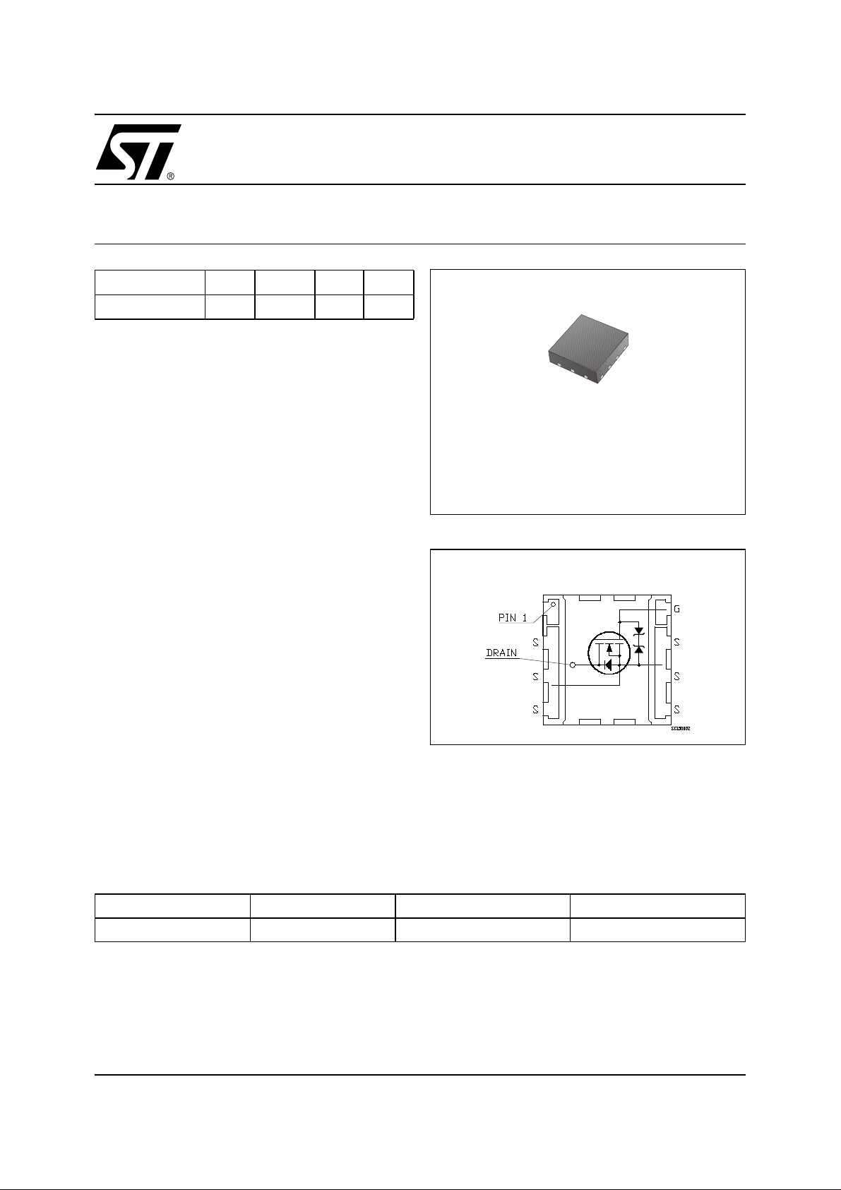
PowerFLAT™(5x5)
(Chip Scale Pa ckage)
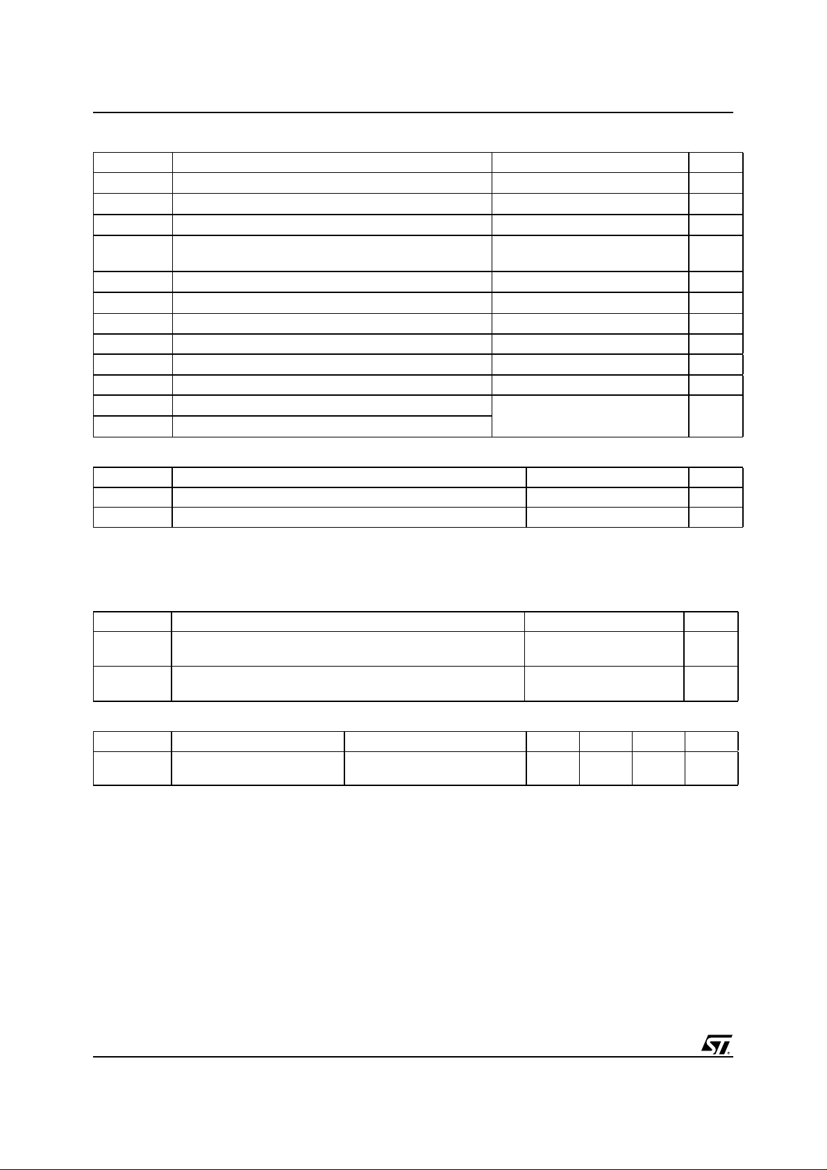
INTERNAL SCHEMATIC DIAGRAM
APPLICATIONS
■ LIGHTING
■ IDEAL FOR OFF-LINE POWER SUPPLIES,
ADAPTORS AND PFC
ORDERING INFORMATION
SALES TYPE MARKING PACKAGE PACKAGING
STL9NK30Z L9NK30Z PowerFLAT™ (5x5) TAPE & REEL
1/8August 2002
Page 2
STL9NK30Z
ABSOLUTE MAXIMUM RATINGS
Symbol Parameter Value Unit
V
DS
V
DGR
V
GS
I
(2) Drain Current (continuous) at TC= 25°C (Steady State)
D
I
DM
P
TOT
P
TOT
V
ESD(G-S)
dv/dt (4) Peak Diode Recovery voltage slope 4.5 V/ns
T
stg
T
j
THERMAL DATA
Symbol Parameter Max. Unit
Rthj-F Thermal Resistance Junction-Foot (Drain) 1.6 °C/W
Rthj-amb (2) Thermal Resistance Junction-ambient 50 °C/W
Note: 1. The value is rated according to R
2. When Mountedon FR-4 Board of 1inch
3. Pulse width limited by safe operating area
4. I
Drain-source Voltage (VGS=0)
Drain-gate Voltage (RGS=20kΩ)
300 V
300 V
Gate- source Voltage ± 30 V
9
Drain Current (continuous) at T
(2)
Drain Current (pulsed) 36 A
= 100°C
C
5.6
(2) Total Dissipation at TC= 25°C (Steady State) 2.5
(1) Total Dissipation at TC= 25°C (Steady State) 75 W
Derating Factor (2) 0.6 W/°C
Gate source ESD(HBM-C=100pF, R=1.5KΩ) 3000 V/ns
Storage Temperature
Max. Operating Junction Temperature
thj-F
< 9A, di/dt<300A/µs, VDD<V
SD
(BR)DSS,TJ<TJMAX
.
2
,2ozCu
–55 to 150 °C
A
A
W
AVALANCHE CHARACTERISTICS
Symbol Parameter Max Value Unit
I
AR
Avalanche Current, Repetitive or Not-Repetitive
(pulse width limited by T
E
AS
Single Pulse Avalanche Energy
(starting T
max)
j
= 25 °C, ID=IAR,VDD=50V)
j
9A
155 mJ
GATE-SOURCE ZENER DIODE
Symbol Parameter Test Conditions Min. Typ. Max. Unit
BV
GSO
Gate-Source Breakdown
Igs=± 1mA (Open Drain) 30 V
Voltage
PROTECTION FEATURES OF GATE-TO-SOURCE ZENER DIODES
The built-in back-to-back Zener diodes have specifically been designed to enhance not only the device’s
ESD capability, but also to make them safely absorb possible voltage transients that may occasionally be
applied from gate to source. In this r es pec t the Zener voltage is appropriate to ac hieve an efficient and
cost-effective intervention to protect the device’s integrity. These integrated Zener diodes thus avoid the
usage of external components.
2/8
Page 3
STL9NK30Z
ELECTRICAL CHARACTERISTICS (TCASE =25°C UNLESS OT HERWISE SPECIFIED)
ON/OFF
Symbol Parameter Test Conditions Min. Typ. Max. Unit
V
(BR)DSS
Drain-source
Breakdown Voltage
I
DSS
I
GSS
V
GS(th)
R
DS(on)
Zero Gate Voltage
Drain Current (V
GS
=0)
Gate-body Leakage
Current (V
DS
=0)
Gate Threshold Voltage
Static Drain-source On
Resistance
DYNAMIC
Symbol Parameter Test Conditions Min. Typ. Max. Unit
(1) Forward Transconductance VDS=10V,ID= 4.5 A 5.4 S
g
fs
Input Capacitance
Output Capacitance
Reverse Transfer
Capacitance
(3) Equivalent Output
C
oss eq.
C
iss
C
oss
C
rss
Capacitance
R
G
Gate Input Resistance f=1 MHz Gate DC Bias = 0
SWITCHING
Symbol Parameter Test Conditions Min. Typ. Max. Unit
t
d(on)
t
d(off)
Q
Q
Q
t
r
t
f
g
gs
gd
Turn-on Delay Time
Rise time
Turn-off Delay Time
Fall Time
Total Gate Charge
Gate-Source Charge
Gate-Drain Charge
ID=1mA,VGS= 0 300 V
V
= Max Rating
DS
VDS= Max Rating, TC= 125 °C
V
= ± 20V ±10 µA
GS
V
DS=VGS,ID
= 50µA
3 3.75 4.5 V
1
50
VGS=10V,ID= 4.5 A 0.36 0.4 Ω
=25V,f=1MHz,VGS= 0 670
V
DS
125
28
VGS=0V,VDS= 0V to 440 V 70 pF
3.6 Ω
Test Signal Level = 20mV
Open Drain
=150V,ID= 4.5 A
V
DD
R
= 4.7Ω VGS=10V
G
(Resistive Load see, Figure 3)
16
20
36
10
=240V,ID=9A,
V
V
DD
GS
=10V
25
5.5
35
13.4
µA
µA
pF
pF
pF
ns
ns
ns
ns
nC
nC
nC
SOURCE DRAIN DIODE
Symbol Parameter Test Conditions Min. Typ. Max. Unit
I
SD
I
SDM
V
SD
t
rr
Q
rr
I
RRM
Note: 1. Pulsed: Pulse duration = 300 µs, duty cycle 1.5 %.
2. Pulse width limited by safe operating area.
3. C
Source-drain Current
(2)
Source-drain Current (pulsed)
(1)
Forward On Voltage
Reverse Recovery Time
Reverse Recovery Charge
Reverse Recovery Current
is defined as a constant equivalent capacitance giving the same charging time as C
oss eq.
.
V
DSS
ISD= 9 A, VGS=0
I
SD
V
DD
(see test circuit, Figure 5)
= 9 A, di/dt = 100A/µs
=40V,Tj= 150°C
165
0.9
11.2
when VDSincreases from 0 to 80%
oss
9
36
1.6 V
A
A
ns
µC
A
3/8
Page 4

STL9NK30Z
Transfer CharacteristicsOutput Characteristics
Transconductance
Gate Charge vs Gate-so urce Voltage
Static Drain-source On Resistance
Capacitance Variations
4/8
Page 5

STL9NK30Z
Normalized Gate Theresho ld Voltage vs Temp.
Source-drain Diode Forward Characteristics
Normalized On Resistance vs Temperature
Normalized BVDSS vs Temperature
5/8
Page 6

STL9NK30Z
Fig. 2: Unclamped Inductive W av eformFig. 1: Unclamped Inductive Load Test Circuit
Fig. 3: Switching Times Test Circuit For
Resistive Loa d
Fig. 5: Test Circuit For Inductive Load Switching
And Diode Recovery Times
Fig. 4: Gate Charge test Circuit
6/8
Page 7

PowerFLAT™(5x5) MECHANICAL DATA
STL9NK30Z
DIM.
MIN. TYP MAX. MIN. TYP. MAX.
A 0.90 1.00 0.035 0.039
A1 0.02 0.05 0.001 0.002
b 0.43 0.51 0.58 0.017 0.020 0.023
c 0.64 0.71 0.79 0.025 0.028 0.031
D 5.00 0.197
E 5.00 0.197
E2 2.49 2.57 2.64 0.098 0.101 0.104
e 1.27 0.050
mm. inch
7/8
Page 8

STL9NK30Z
Information furnished is believed to be accurate and reliable. However, STMicroelectronics assumes no responsibility f or t he
consequences of use of su ch in formation nor for any in fringement of patents or other rights of third parties w hich may result from
its use. No license is granted by implication or otherwise under any patent or patent rights of STMicroelectronics. Specifications
mentioned in this publication are subject to change without notice. This publication supersedes and replaces all information
previously suppli ed. STMi croelect ronics pr oducts are not author ized for use as cr itical component s in li fe suppo rt devi ces or
systems without express written approval of STMicroelectronics.
Australia - Brazil - Canada - China - Finland - France - Germany - Hong Kong - India - Israel - Italy - Japan - Malaysia - Malta - Morocco
© The ST logo is a registered trademark of STMicroelectronics
© 2002 STMicroelectronics - Printed in Italy - All Rights Reserved
Singapore - Spain - Sweden - Switzerland - United Kingdom - United States.
STMicroelectronics GROUP OF COMPANIES
© http://www.st.com
8/8
 Loading...