

Page 1
STL34NF06
N-CHANNEL 60V - 0.024Ω -34APowerFLAT™
LOW GATE CHARGE STripFET™II MOSFET
PRELIMINARY DATA
TYPE V
STL34NF06 60 V < 0.028Ω 34 A
TYPICAL RDS(on) = 0.024Ω
IMPROVED DIE-TO-FOOTPRINT RATIO
VERY LOW PROFILE PACKAGE
DSS
R
DS(on)
I
D
DESCRIPTION
This Power MOSFET is t he s ec ond generation of
STMicroelectronics unique “STripFET™” tec hnology.The resulting transistor shows extremely low onresistance and minimal gate charge. The new PowerFLAT™ package allow a significant reduction in
board space without compramising performance.
APPLICATIONS
DC-DC CONVERTERS
BATTERY MANAGEMENT IN NOMADIC
EQUIPMENT
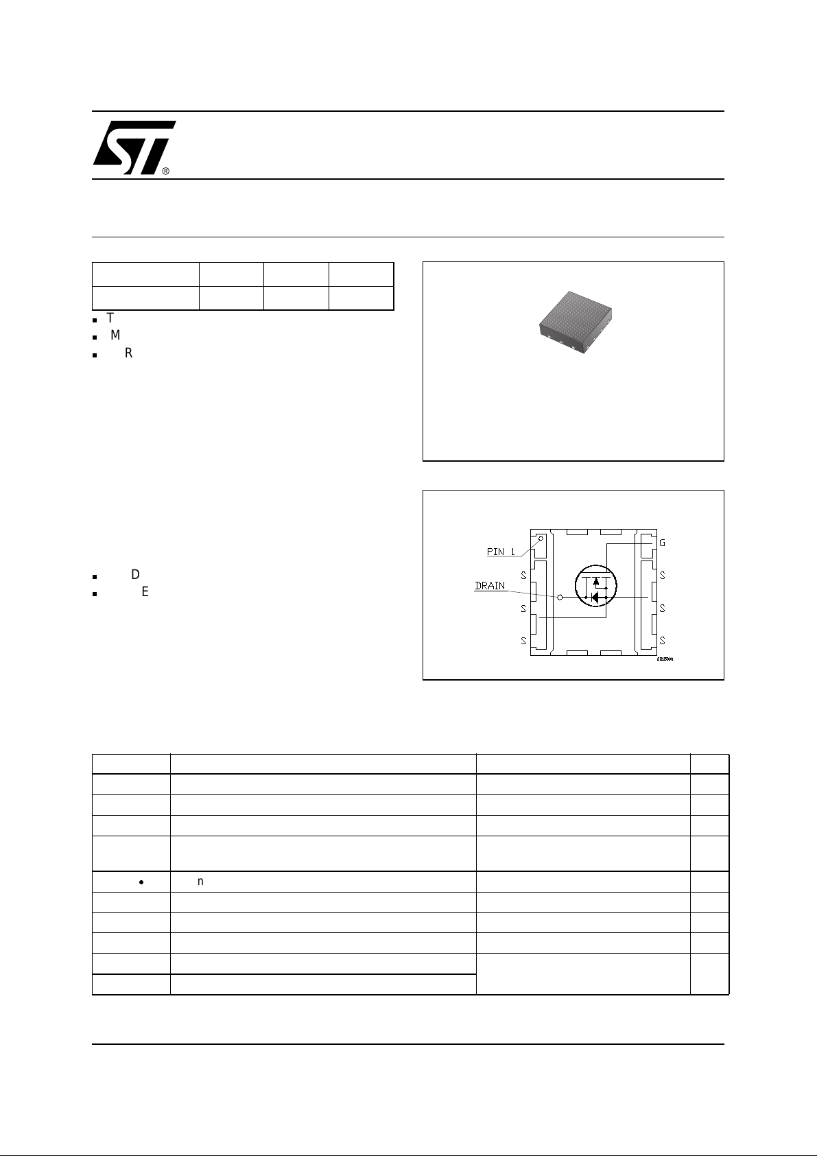
PowerFLAT™(5x5)
(Chip Scale Package)
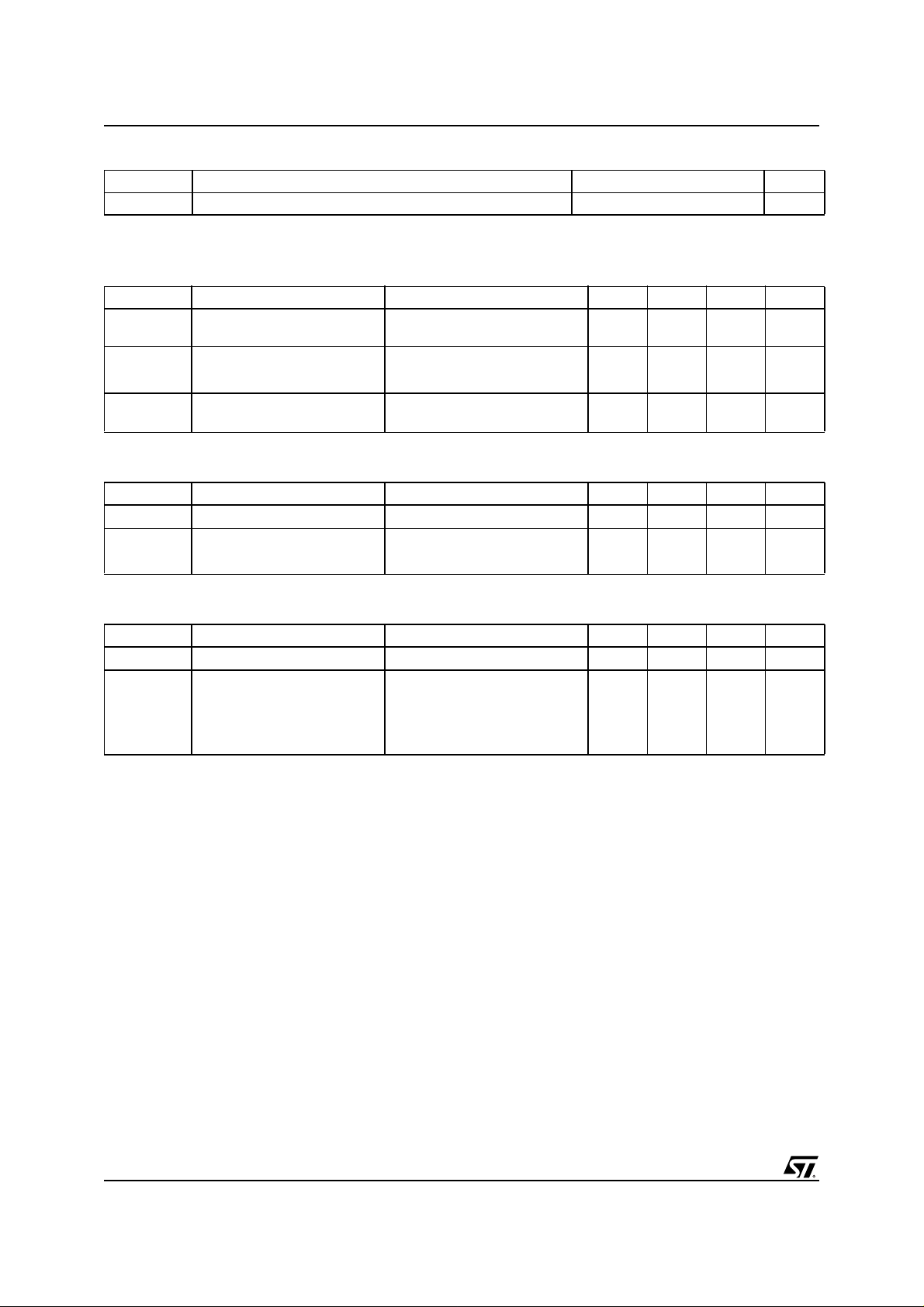
INTERNAL SCHEMATIC DIAGR AM
ABSOLUTE MAXIMUM RATINGS
Symbol Parameter Value Unit
V
DS
V
DGR
V
GS
I
D
I
DM
P
TOT
E
AS
T
stg
T
j
(•)Pulse width limited by safe operating area
(*) Current Limited by Wire Bonding is 20A
November 2002
Drain-source Voltage (VGS=0)
Drain-gate Voltage (RGS=20kΩ)
Gate- source Voltage ± 20 V
Drain Current (continuous) at TC= 25°C (*)
Drain Current (continuous) at TC= 100°C
()
Drain Current (pulsed) 136 A
Total Dissipation at TC= 25°C
Derating Factor 0.56 W/°C
(1)
Single Pulse Avalanche Energy 250 mJ
Storage Temperature
Max. Operating Junction Temperature
(1) Starting Tj=25°C,ID=17A,VDD= 42V
60 V
60 V
34
20
70 W
–55 to 150 °C
A
A
1/6
Page 2
STL34NF06
THERMAL DATA
Rthj-case Thermal Resistance Junction-case Max 1.8 °C/W
Rthj-pcb (#) Thermal Resistance Junction-ambient Max 31.2 °C/W
(*) When mounted on 1inch² FR4 Board, 2oz of Cu, t ≤ 10 sec.
ELECTRICAL CHARACTERISTICS (T
= 25 °C UNLESS OTHERWISE SPECIFIED)
CASE
OFF
Symbol Parameter Test Conditions Min. Typ. Max. Unit
V
(BR)DSS
Drain-source
ID= 250 µA, VGS= 0 60 V
Breakdown Voltage
I
DSS
I
GSS
Zero Gate Voltage
Drain Current (V
GS
Gate-body Leakage
Current (V
DS
=0)
=0)
V
= Max Rating
DS
VDS= Max Rating, TC= 125 °C
V
= ± 20V ±100 nA
GS
1µA
10 µA
ON (1)
Symbol Parameter Test Conditions Min. Typ. Max. Unit
V
GS(th)
R
DS(on)
Gate Threshold Voltage
Static Drain-source On
V
DS=VGS,ID
VGS=10V,ID=17A
= 250µA
2V
0.024 0.028 Ω
Resistance
DYNAMIC
Symbol Parameter Test Conditions Min. Typ. Max. Unit
(1) Forward Transconductance VDS=30V,ID= 17 A TBD S
g
fs
C
iss
C
oss
C
rss
Input Capacitance
Output Capacitance 225 pF
Reverse Transfer
Capacitance
1. Pulsed:Pulse duration = 300 µs, duty cycle1.5%.
V
=25V,f=1MHz,VGS=0
DS
920 pF
80 pF
2/6
Page 3

STL34NF06
ELECTRICAL CHARACTERISTICS (CONTINUED)
SWITCHING ON
Symbol Parameter Test Conditions Min. Typ. Max. Unit
V
t
d(on)
Q
Q
Q
t
r
gs
gd
Turn-on Delay Time
Rise Time 50 ns
Total Gate Charge
g
Gate-Source Charge 6.5 nC
Gate-Drain Charge 14.4 nC
SWITCHING OFF
Symbol Parameter Test Conditions Min. Typ. Max. Unit
t
d(off)
t
f
Turn-Off-Delay Time
Fall Time 11 ns
SOURCE DRAIN DIODE
Symbol Parameter Test Conditions Min. Typ. Max. Unit
(3)
I
I
SDM
V
SD
SD
Q
I
RRM
t
rr
rr
Source-drain Current 34 A
(2)
Source-drain Current (pulsed) 136 A
(1)
Forward On Voltage
Reverse Recovery Time
Reverse Recovery Charge 151 nC
Reverse Recovery Current 4.8 A
=30V,ID=17A
DD
= 4.7Ω VGS=10V
R
G
(see test circuit, Figure 3)
V
=48V,ID=34A,
DD
VGS=10V
V
=30V,ID= 17A,
DD
= 4.7Ω, VGS=10V
R
G
(see test circuit, Figure 3)
ISD=34A,VGS=0
I
= 34 A, di/dt = 100A/µs,
SD
V
=10V,Tj=150°C
DD
(see test circuit, Figure 5)
11 ns
32 43 nC
27 ns
1.2 V
63 ns
Note: 1. Pulsed: Pulse duration = 300 µs, duty cycle 1.5 %.
2. Pulse width limited by safe o perating area.
3. Current Limited by Wire Bonding is 20A
3/6
Page 4

STL34NF06
Fig. 2: Unclamped Inductive Wav eformFig. 1: Unclamped Inductive Load Test Circuit
Fig. 3: Switching Times Test Circuit For
Resistive Loa d
Fig. 5: Test Circuit For Inductive Load Switching
And Diode Recovery Times
Fig. 4: Gate Charge test Circuit
4/6
Page 5

PowerFLAT™(5x5) MECHANICAL DATA
STL34NF06
DIM.
MIN. TYP MAX. MIN. TYP. MAX.
A 0.90 1.00 0.035 0.039
A1 0.02 0.05 0.001 0.002
b 0.43 0.51 0.58 0.017 0.020 0.023
c 0.33 0.41 0.48 0.013 0.016 0.019
D 5.00 0.197
E 5.00 0.197
E2 3.10 3.18 3.25 0.122 0.125 0.128
e 1.27 0.050
mm. inch
5/6
Page 6

STL34NF06
Information furnished is believed to be accurate and reliable. However, STMicroelectronics assumes no responsibility f or t he
consequences of use of su ch in formation nor for any in fringement of patents or other rights of third parties w hich may result from
its use. No license is granted by implication or otherwise under any patent or patent rights of STMicroelectronics. Specifications
mentioned in this publication are subject to change without notice. This publication supersedes and replaces all information
previously suppli ed. STMi croelect ronics pr oducts are not author ized for use as cr itical component s in li fe suppo rt devi ces or
systems without express written approval of STMicroelectronics.
Australia - Brazil - Canada - China - Finland - France - Germany - Hong Kong - India - Israel - Italy - Japan - Malaysia - Malta - Morocco
© The ST logo is a registered trademark of STMicroelectronics
© 2002 STMicroelectronics - Printed in Italy - All Rights Reserved
Singapore - Spain - Sweden - Switzerland - United Kingdom - United States.
STMicroelectronics GROUP OF COMPANIES
© http://www.st.com
6/6
 Loading...