

Page 1
STL30NF3LL
N-CHANNEL 30V - 0.008Ω - 30A PowerFLAT ™
LOW GATE CHARGE STripFET™ MOSFET
PRELIMINARY DATA
TYPE V
DSS
R
DS(on)
I
D
STL30NF3LL 30 V < 0.010 Ω 30 A
■ TYPICAL R
■ IMPROVED DIE-TO-FOOTPRINT RATIO
■ VERY LOW PROFILE PACKAGE
(on) = 0.008Ω
DS
DESCRIPTION
This Power MOSFET is t he second generation of
STMicroelectronics unique “STripFET™” technology. The resulting transistor shows extremely low onresistance and minimal gate charge. The new PowerFLAT™ package allows a significant reduction in
board space without compromising performance.
APPLICATIONS
■ DC-DC CONVERTERS
■ BATTERY MANAGEMENT IN NOMADIC
EQUIPMENT
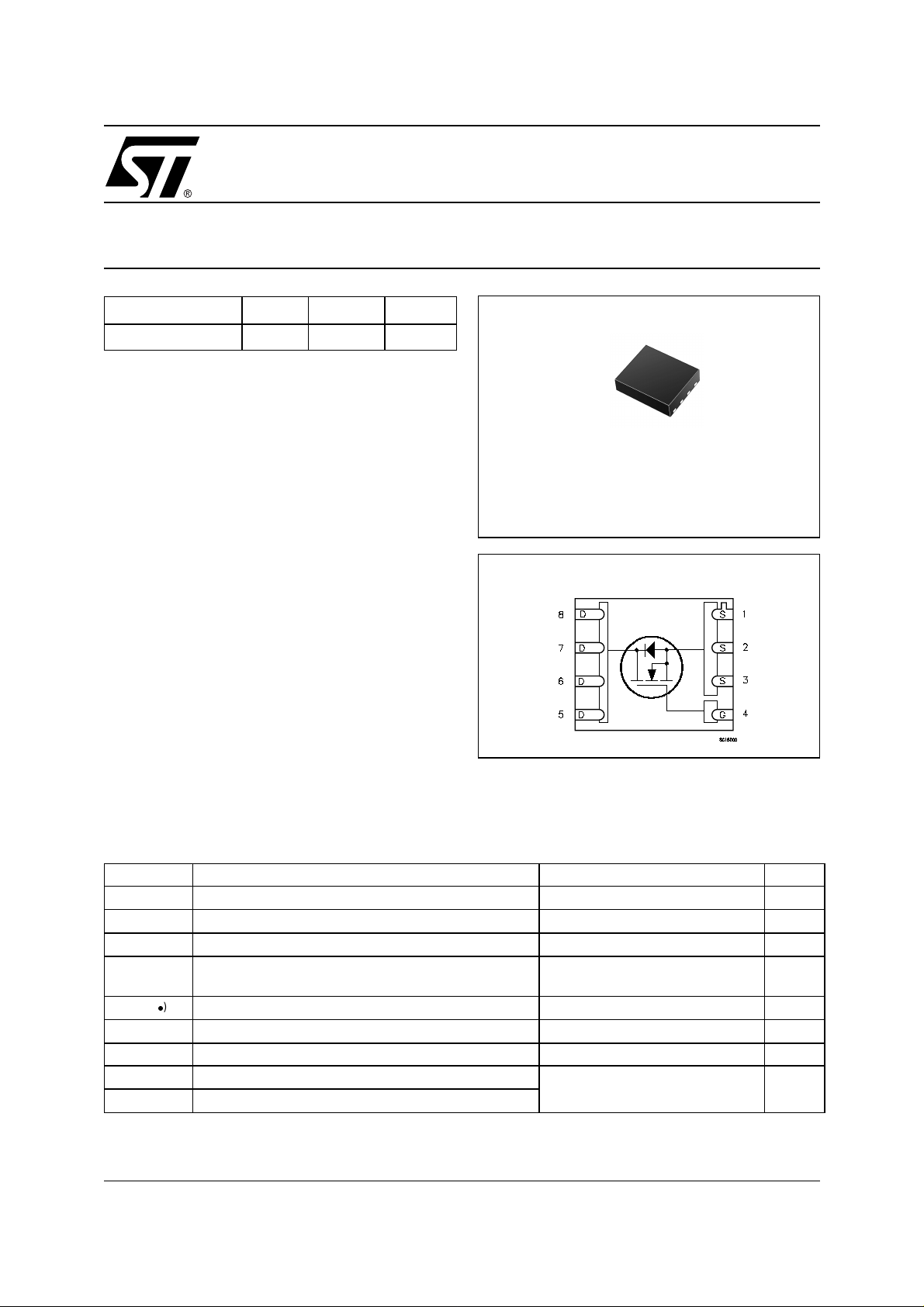
PowerFLAT™(6x5)
(Chip Scale Package)
INTERNAL SCHEMATIC DIAGRAM
ABSOLUTE MAXIMUM RATINGS
Symbol Parameter Value Unit
V
DS
V
DGR
V
GS
I
(#) Drain Current (continuos) at TC = 25°C
D
I
DM
P
TOT
T
stg
T
j
(●) Pulse width limited by safe operating area
(#) Limited by Wire Bonding
November 2001
Drain-source Voltage (VGS = 0)
Drain-gate Voltage (RGS = 20 kΩ)
30 V
30 V
Gate- source Voltage ± 16 V
30
Drain Current (continuos) at T
(l)
Drain Current (pulsed) 120 A
Total Dissipation at TC = 25°C
= 100°C
C
19
80 W
Derating Factor 0.64 W/°C
Storage Temperature
Max. Operating Junction Temperature
– 55 to 150 °C
A
A
1/6
Page 2
STL30NF3LL
THERMA L D ATA
Rthj-case Thermal Resistance Junction-case Max 1.56 °C/W
Rthj-amb Thermal Resistance Junction-ambient Max 50 °C/W
ELECTRICAL CHARACTERISTICS (TCASE = 25 °C UNLESS OTHERWISE SPECIFIED)
OFF
Symbol Parameter Test Conditions Min. Typ. Max. Unit
V
(BR)DSS
Drain-source
Breakdown Voltage
Zero Gate Voltage
Drain Current (V
GS
Gate-body Leakage
Current (V
DS
= 0)
= 0)
ON
I
DSS
I
GSS
(1)
Symbol Parameter Test Conditions Min. Typ. Max. Unit
V
GS(th)
R
DS(on)
Gate Threshold Voltage
Static Drain-source On
Resistance
ID = 250 µA, VGS = 0 30 V
V
= Max Rating
DS
V
= Max Rating, TC = 125 °C
DS
V
= ± 16V ±100 nA
GS
V
= VGS, ID = 250µA
DS
VGS = 10 V, ID = 15 A
VGS = 4.5 V, ID = 15A
1V
0.008 0.010 Ω
0.0095 0.013 Ω
1µA
10 µA
DYNAMIC
Symbol Parameter Test Conditions Min. Typ. Max. Unit
(1) Forward Transconductance VDS = 15V, ID= 15 A 30 S
g
fs
C
iss
C
oss
C
rss
Input Capacitance
Output Capacitance 635 pF
Reverse Transfer
Capacitance
V
= 25 V, f = 1 MHz, VGS = 0
DS
2210 pF
138 pF
2/6
Page 3

STL30NF3LL
ELECTRICAL CHARACTERISTICS (CONTINUED)
SWITCHING ON
Symbol Parameter Test Conditions Min. Typ. Max. Unit
V
t
d(on)
Q
Q
Q
t
r
g
gs
gd
Turn-on Delay Time
Rise Time 130 ns
Total Gate Charge
Gate-Source Charge
Gate-Drain Charge
SWITCHING OFF
Symbol Parameter Test Conditions Min. Typ. Max. Unit
t
d(off)
t
f
Turn-off-Delay Time
Fall Time
SOURCE DRAIN DIODE
Symbol Parameter Test Conditions Min. Typ. Max. Unit
I
SD
I
SDM
VSD (1)
t
rr
Q
rr
I
RRM
Note: 1. Pulsed: Pu l se duration = 300 µs, duty c yc l e 1.5 %.
2. Pulse width li mited by safe operating area.
Source-drain Current 30 A
(2)
Source-drain Current (pulsed) 120 A
Forward On Voltage
Reverse Recovery Time
Reverse Recovery
ChargeReverse Recovery
Current
= 15 V, ID = 30 A
DD
R
= 4.7Ω VGS = 4.5V
G
(see test circuit, Figure 1)
VDD = 24 V, ID = 30 A,
VGS = 5 V
(see test circuit, Figure 1)
VDD = 15 V, ID = 30 A,
RG=4.7Ω, V
GS
= 4.5 V
(see test circuit, Figure 1)
ISD = 15 A, VGS = 0
= 30 A, di/dt = 100A/µs,
I
SD
VDD = 15 V, Tj = 150°C
(see test circuit, Figure 3)
22 ns
30
40 nC
9
12.5
36.5
36.5
1.2 V
65
105
3.4
nC
nC
ns
ns
ns
nC
A
3/6
Page 4

STL30NF3LL
Resistive Load
Fig. 3: Test Circuit For Diode Recovery Behaviour
Fig. 2: Gate Charge test CircuitFig. 1: Switching Times Test Circuit For
4/6
Page 5

PowerFLAT™(6x5) MECHA NICA L DATA
STL30NF3LL
DIM.
MIN. TYP MAX. MIN. TYP. MAX.
A 0.80 1.00 0.031 0.039
A1 0.02 0.001
b 0.35 0.47 0.014 0.018
C 1.61 0.063
D 5.00 0.197
D2 4.15 4.25 0.163 0.167
E 6.00 0.236
E2 3.55 3.65 0.140 0.144
e 1.27 0.049
F 1.99 0.078
G 2.20 0.086
H 0.40 0.015
I 0.219 0.0086
L 0.70 0.90 0.028 0.035
mm. inch
5/6
Page 6

STL30NF3LL
6/6
Information furnished is believed to be accurate and reliable. However, STMicroelectronics assumes no responsibility for the consequences
of use of such informa tion n or for an y infring ement of patent s or other rig hts of third part ies which may resu lt from its use . No l i cen se i s
granted by implication or otherwise under any patent or patent rights of STMicroelectronics. Specification mentioned in this publication are
subject to change without notice. This publication supersedes and replaces all information previously supplied. STMicroelectronics products
are not authorized for use as critical compo nents in life support devices or systems without express written approval of STMicroelectronics.
Australia - Brazil - China - Finland - France - Germany - Hong Kong - India - Italy - Japan - Malaysia - Malta - Morocco -
The ST logo is a trademark of STMicroelectronics
© 2001 STMicroelectronics – Printed in Italy – All Rights Reserved
STMicroelectronics GROUP OF COMPANIES
Singapore - Spain - Sweden - Switzerland - United Kingdom - U.S.A.
http://www.st.com
 Loading...