

Page 1
STL22NF10
N-CHANNEL 100V - 0.055 Ω - 22A PowerF LAT™
LOW GATE CHARGE STripFET™ II MOSFET
TYPE
V
DSS
STL22NF10 100 V <0.060
■ TYPICAL R
■ IMPROVED DIE-TO-FOOTPRINT RATIO
■ VERY LOW PROFILE PACKAGE (1mm MAX)
■ VERY LOW THERMAL RESISTANCE
■ VERY LOW GATE CHARGE
(on) = 0.055 Ω
DS
R
DS(on)
I
D
22 A
(1)
Ω
DESCRIPTION
This application speci fic Power MOSFET is the second
generation of STMicroelectronis unique "STripFET™"
technology. The resulting trans istor s hows extre mely l ow
on-resistance and minimal gate charge. The new
PowerFLAT™ pac kage allows a significant reduction in
board space without compromising performance.
APPLICATIONS
■ HIGH-EFFICIENCY ISOLATED DC-DC
CONVERTERS
■ TELECOM AND AUTOMOTIVE
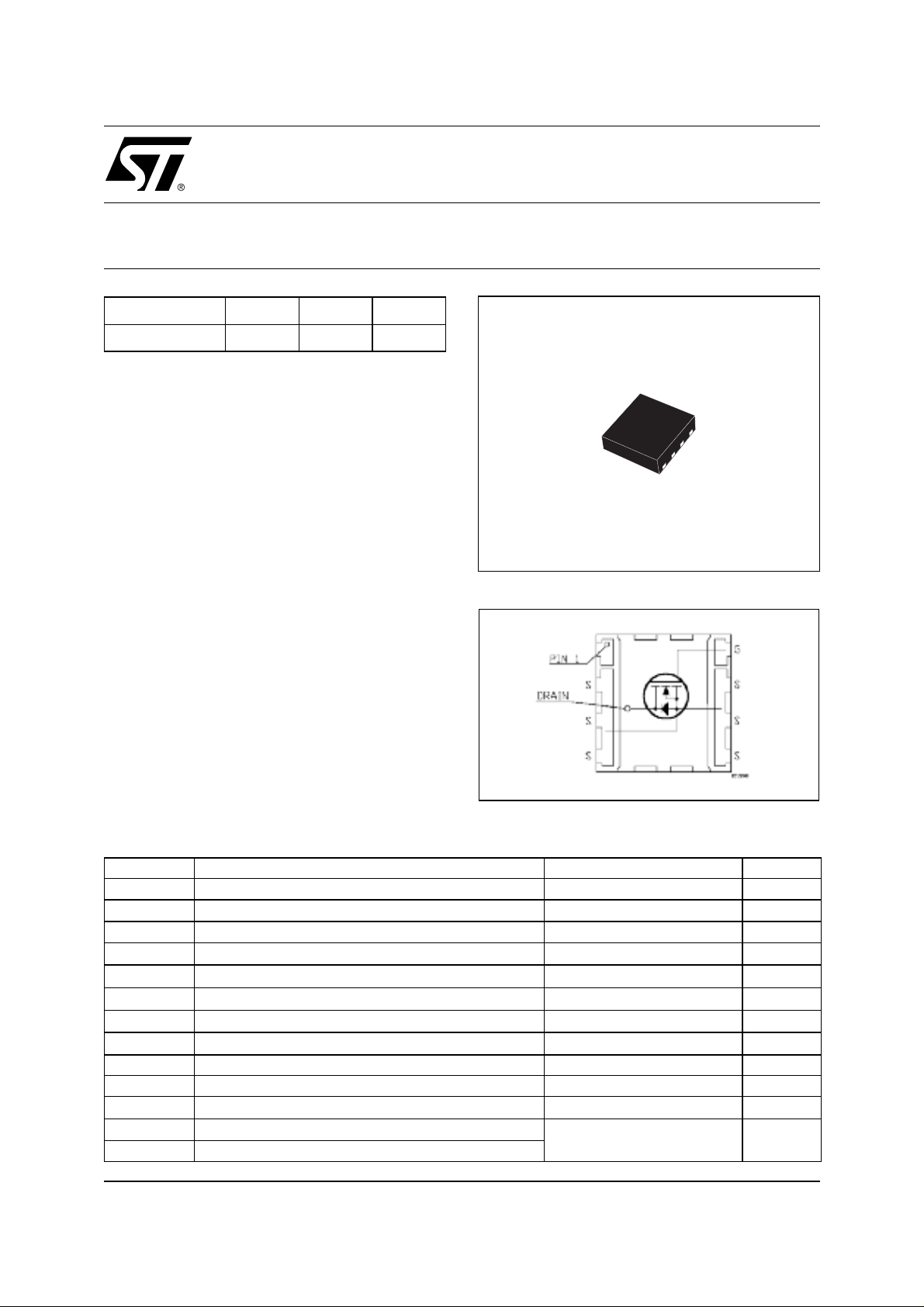
PowerFLAT™(5x5)
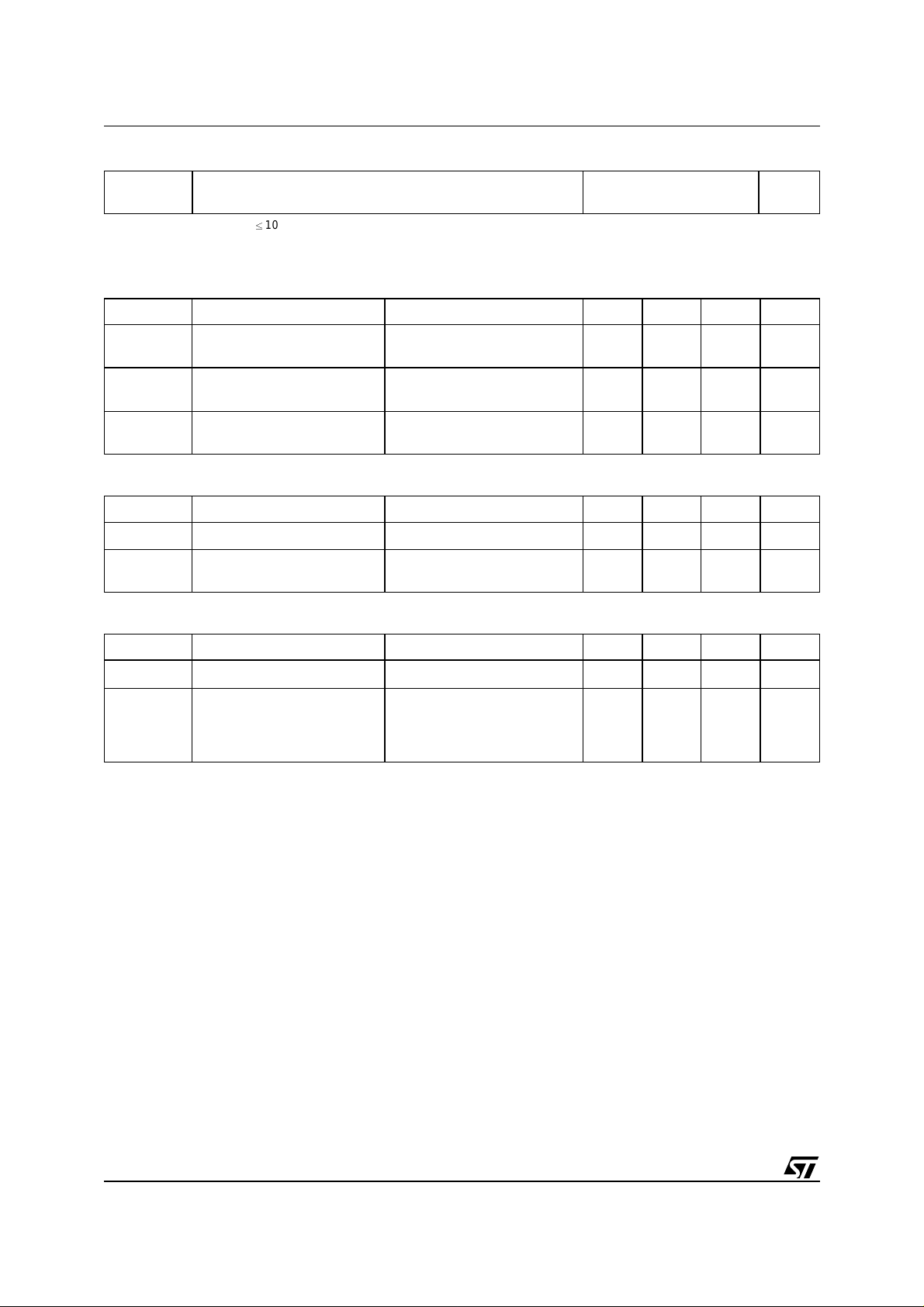
INTERNAL SCHEMATIC DIAGRAM
ABSOLUTE MAXIMUM RATINGS
Symbol Parameter Value Unit
V
DS
V
DGR
V
GS
(2)
I
D
(2)
I
D
(3)
I
DM
(2)
P
tot
(1)
P
tot
dv/dt
E
AS
T
stg
T
j
.
Drain-source Voltage (VGS = 0)
Drain-gate Voltage (RGS = 20 kΩ)
100 V
100 V
Gate- source Voltage ± 20 V
Drain Current (continuous) at TC = 25°C (Steady State)
Drain Current (continuous) at TC = 100°C
5.3 A
3.8 A
Drain Current (pulsed) 22 A
Total Dissipation at TC = 25°C (Steady State)
Total Dissipation at TC = 25°C
4W
70 W
Derating Factor 0.03 W/°C
(5)
Peak Diode Recovery voltage slope 16 V/ns
(6)
Single Pulse Avalanche Energy 82 mJ
Storage Temperature
Operating Junction Temperature
-55 to 150 °C
1/8February 2003
Page 2
STL22NF10
THERMAL DATA
Rthj-F
Rthj-pcb(4)
(*)
Mounte d on F R-4 board (t [ 10 se c.)
(*)Thermal Resistance Junction-Foot (Drain)
Thermal Operating Junction-pcb
1.8
31.5
°C/W
°C/W
ELECTRICAL CHARACTERISTICS (T
= 25 °C unless otherwise specified)
case
OFF
Symbol Parameter Test Conditions Min. Typ. Max. Unit
I
V
(BR)DSS
Drain-source
= 250 µA, VGS = 0
D
100 V
Breakdown Voltage
V
= Max Rating
DS
V
= Max Rating TC = 125°C
DS
V
= ± 20 V
GS
1
10
±100 nA
ON
(7)
I
DSS
I
GSS
Zero Gate Voltage
Drain Current (V
GS
Gate-body Leakage
Current (V
DS
= 0)
= 0)
Symbol Parameter Test Conditions Min. Typ. Max. Unit
V
GS(th)
R
DS(on)
Gate Threshold Voltage
Static Drain-source On
= VGS I
DS
V
= 10 V ID = 11 A
GS
= 250 µA
D
2V
0.055 0.060
V
Resistance
DYNAMIC
Symbol Parameter Test Conditions Min. Typ. Max. Unit
(7)
g
fs
C
iss
C
oss
C
rss
Forward Transconductance
Input Capacitance
Output Capacitance
Reverse Transfer
Capacitance
V
20 V ID= 11 A
DS =
= 25V, f = 1 MHz, VGS = 0
V
DS
16 S
885
130
56
µA
µA
Ω
pF
pF
pF
2/8
Page 3
STL22NF10
ELECTRICAL CHARACTERISTICS (continued)
SWITCHING ON
Symbol Parameter Test Conditions Min. Typ. Max. Unit
= 50 V ID = 11 A
t
d(on)
Turn-on Delay Time
t
r
Rise Time
V
DD
R
= 4.7 Ω VGS = 10 V
G
(Resistive Load, Figure 3)
Q
g
Q
gs
Q
gd
Total Gate Charge
Gate-Source Charge
Gate-Drain Charge
= 80V ID= 22A VGS=10V
V
DD
SWITCHING OFF
Symbol Parameter Test Conditions Min. Typ. Max. Unit
= 50 V ID = 11 A
t
d(off)
Turn-off Delay Time
t
f
Fall Time
V
DD
R
= 4.7Ω, V
G
GS
= 10 V
(Resistive Load, Figure 3)
SOURCE DRAIN DIODE
Symbol Parameter Test Conditions Min. Typ. Max. Unit
I
SD
I
SDM
V
SD
t
rr
Q
rr
I
RRM
(1)
The value is rated accordin g R
(2)
The value is rated accordin g R
(3)
Pulse width limited by safe operating area.
(4)
When Mount ed on FR-4 Board of 1 in ch², 2 oz Cu, t<10s.
(5)
ISD ≤22A, di/dt ≤300A/µs, VDD ≤ V
(6)
Starting Tj = 25 oC, ID = 11 A, VDD = 30V.
(7)
Pulsed: Pulse duration = 300 µs, duty cycle 1.5 %.
Source-drain Current
Source-drain Current (pulsed)
(7)
Forward On Voltage
Reverse Recovery Time
Reverse Recovery Charge
Reverse Recovery Current
thj-F
thj-pcb
.
.
(BR)DSS
, Tj ≤ T
I
= 22 A VGS = 0
SD
=22 A di/dt = 100A/µs
I
SD
V
= 30 V Tj = 150°C
DD
(see test circuit, Figure 5)
.
JMAX
20
45
30
6
10
45
10
100
375
7.5
40 nC
5.3
22
1.3 V
ns
ns
nC
nC
ns
ns
A
A
ns
nC
A
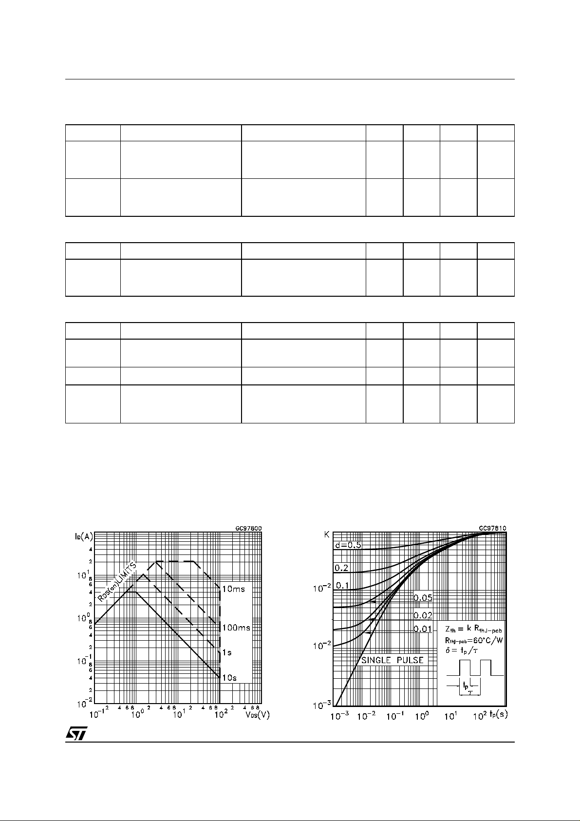
Safe Operating Area
Thermal Impedance
3/8
Page 4

STL22NF10
Output Characteristics Transfer Characteristics
Transconductance Static Drain-source On Resistance
Gate Charge vs Gate-source Voltage Capacitance Variations
4/8
Page 5

STL22NF10
Normalized Gate Threshold Voltage vs Temperature Normalized on Resistance vs Temperature
Source-drain Diode Forward Characteristics Normalized Breakdown Voltage vs Temperature.
. .
5/8
Page 6

STL22NF10
Fig. 1: Unclamped Inductive Load Test CircuitFig. 1: Unclamped Inductive Load Test Circuit Fig. 2: Unclamped Inductive Waveform
Fig. 3: Switching Times Test Circuits For Resistive
Load
Fig. 5: Test Circuit For Inductive Load Switching
And Diode Recovery Times
Fig. 4: Gate Charge test Circuit
6/8
Page 7

STL22NF10
7/8
Page 8

STL22NF10
Information furnished is believed to be accurate and reliable. However, STMicroelectronics assumes no responsibility for the consequences
of use of such information nor for any infringement of patents or other rights of third parties which may result from its use. No license is granted
by implic ation or otherw i se under any patent or patent rights of S T M i croelectronic s. Specificati ons mentione d i n this publication are subject
to change without notice. This publication supersedes and replaces all information previously supplied. STMicroelectronics products are not
authorized for use as criti cal components in li fe support devi ces or systems without express written approval of STM i croelectronics.
The ST logo is registered trademark of STMicroelectronics
2003 STMi croelectronics - All Rights Reserved
All other na m es are the proper ty of their respective owners.
Australi a - Brazil - Canada - China - Finlan d - F rance - German y - H ong Kong - India - Is rael - Italy - Japan - Malaysia - Mal ta - Morocco -
Singap ore - Spain - Sweden - Switzerla nd - United Kingdom - United States .
STMicroelectronics GROUP OF COMPANIES
http:// www.st.com
8/8
 Loading...