

Page 1

LCD Controller 1/20 Issue date : 22 September,1999
Syntek Semiconductor Co., Ltd.
STK85C161
Specification
1. FEATURES :
* Operating voltage : 2.5V – 3.5 V.
* Maximum CPU operating frequency : 2MHz at 2.7V
* Oscillators :
- RC or 32.768 KHz crystal oscillator for LCD display and watch timer.
- Built-in PLL circuit to generate 4.19MHz system clock.
* 40 segments and 4 commons output for LCD driver.
- 1/3 bias, 1/4 duty and 64Hz frame frequency.
* 20 I/O pins.
- 8 I/O pins with selectable wake up interrupt.
- 4 general I/O pins.
- 8 I/O pin shared with S32-S39.
* Built in 160 bytes data RAM and 20 bytes write-only RAM for LCD display.
* Built in 96K bytes ROM with 16K bytes per bank for program.
* One 8-bit timer with 8 predefined input clock.
* Two sound generators and one voice channel with PWM outputs.
* Seven interrupt sources :
NMI - 64 Hz interrupt
IRQ1 - Fix-time timer interrupt
IRQ2 - Timer 1 interrupt
IRQ3 - External interrupt
IRQ4 - Timer 2 interrupt
IRQ5 - Sound generator 1 interrupt
IRQ6 - Sound generator 2 interrupt
* Code option :
- Built-in 150K OHM pull-up resistors for I/O port.
- RC or 32768Hz crystal oscillation for LCD driver.
2. APPLICATION :
* Talking Calculator
* Talking clock
* Hand-held game
Page 2

LCD Controller 2/20 Issue date : 22 September,1999
Syntek Semiconductor Co., Ltd.
STK85C161
* Small instrument
3. BLOCK DIAGRAM :
A0-A15 IRQ
D0-D7
P10-P17 P20-P23 PWM1 PWM2
8-bit CPU
Address
decoder
ROM
96Kx8
RAM
160x8
Clock
Generator
LCD driver
8-bit Timer
Port 1
Two sound generators
and one voice channel
PLL
32768Hz
C0-C3
S0-S39
VCAP
LCD RAM
20x8
Port 2
Page 3

LCD Controller 3/20 Issue date : 22 September,1999
Syntek Semiconductor Co., Ltd.
STK85C161
4. PIN DESCRIPTION : (Total 72 pads)
Pin name I/O Function description
COM0-COM3 O LCD common output pins
SEG0-SEG39 O LCD segment output pins
P10-P17 I/O 8-bit I/O pins for port 1
P20-P23 I/O 4-bit I/O pins for port 2. P23 can be set as output with
carrier clock.
P30-P37 I/O 8-bit I/O pins for port 3. These pins are shared with
S32-S39.
VCAP I/O Low pass filter capacitor for PLL.
XOSC1 I 32.768K Hz crystal oscillator input
XOSC2 O 32.768K Hz crystal oscillator output
PWM1
PWM2
O Sound channel PWM output with volume control.
/RES I System reset pin with 100K pull-up resistor.
VLCD I Bias voltage input pin.
VC2 I 2/3Vlcd bias voltage input pin.
VC1 I 1/3Vlcd bias voltage input pin.
C1A, C1B Booster capacitor connection pins
C2A, C2B Booster capacitor connection pins
/TEST I Test pin. Keep floating or connect to Vdd
VDD1 Power input for PWM output
VSS1 Signal ground for PWM output
VDD Power input
VSS Signal ground
Page 4

LCD Controller 4/20 Issue date : 22 September,1999
Syntek Semiconductor Co., Ltd.
STK85C161
5. ADDRESS ARRANGEMENT
1) LCD Data latches
0000-001C for LCD output data storage. The memory addresses, which are not specified in
the table, are not implemented. This area is write only.
SEG0-SEG7 SEG8-SEG15 • • • SEG31-SEG39
COM0 0000 0001 • • • 0004
COM1 0008 0009 • • • 000C
COM2 0010 0011 • • • 0014
COM3 0018 0019 • • • 001C
The LSB of low byte – SEG0.
The MSB of high byte – SEG39.
The middle bits are in the order.
2) RAM
0040-00DF for zero page area.
0140-01DF for stacks. This area is overlapped with 0040-00DF.
3) ROM
8000-BFFF For program bank area.
C000-FFFF for program area. This area is always mapping to the last 16K bytes of internal
ROM and it is not affected by the bank setting.
FFFF, FFFE - IRQ vector.
FFFD, FFFC - RES vector.
FFFB, FFFA - NMI vector.
4) Others
1000 To enter stand-by mode. Write only.
* Write this address, the CPU will be hold with LCD state no change.
* When in stand-by mode, the NMI and IRQ will wake up the CPU.
1001 To enter sleep mode. Write only.
Bit 0 = 1 Sleep mode 1
Page 5

LCD Controller 5/20 Issue date : 22 September,1999
Syntek Semiconductor Co., Ltd.
STK85C161
1 = 1 Sleep mode 2
In sleep mode 1, both of the main system oscillator and 32.768KHz sub-system
oscillator will be stopped. So, all functions are stopped and only external interrupt can
wake up this chip. The LCD display will be turn off while getting into sleep mode 1. If
the LCD is turned on after wake-up immediately, then some garbage may display on the
LCD. It is better to turn off the LCD by software before enter sleep mode 1. After wake
up, the software has to delay several ms before turn on the LCD because the crystal will
take several mS to stable.
In sleep mode 2, only main system oscillator will be stopped. So, the following functions
will still keep working.
* The LCD will be kept on.
* The fix-time timer will keep going.
* The NMI, port 1, and fix-time timer interrupt will wake up this chip.
* CPU will keep working if clock source is 32.768K Hz.
1002 Watch timer control register. Write only.
Bit 1 : = 0 Set fix-time timer interrupt at 2 Hz
= 1 Set fix-time timer interrupt at 1 Hz
7-2 : Reserved.
The default values for each bit is zero.
1003 IRQ flag register. Read & write.
Read function :
Bit 0 : = 1 Fix-time timer interrupt, IRQ1.
1 : = 1 Timer 1 interrupt, IRQ2.
2 : = 1 Port 1 interrupt, IRQ3.
3 : = 1 Timer 2 interrupt, IRQ4.
4 : = 1 Sound generator 1 (timer3) interrupt, IRQ5.
5 : = 1 Sound generator 2 (timer4) interrupt, IRQ6.
Write function :
Bit 0 : = 0 Clear fix-time timer interrupt.
1 : = 0 Clear timer 1 interrupt.
2 : = 0 Clear port 1 interrupt.
3 : = 0 Clear timer 2 interrupt.
4 : = 0 Clear sound generator 1 (timer3) interrupt.
Page 6

LCD Controller 6/20 Issue date : 22 September,1999
Syntek Semiconductor Co., Ltd.
STK85C161
5 : = 0 Clear sound generator 2 (timer4) interrupt.
* Before firmware exits the interrupt routine, the interrupt flag must be cleared.
Otherwise, the IC will get into interrupt again.
* Write 0 to clear the corresponding IRQ.
* Do NOT use TRB to test and clear this register. Following instructions are
recommended.
LDA $1003
AND #1 ;If IRQ 1 is checking.
BEQ next_irq
EOR #0FFH
STA $1003 ;Clear the active interrupt.
1004 Port 1 data. Read & write.
Page 7

LCD Controller 7/20 Issue date : 22 September,1999
Syntek Semiconductor Co., Ltd.
STK85C161
1005 Set port 1 bit function. Write only.
* An '1' in this register will set the corresponding pin of port 1 as an output pin.
* The default values for each bit is zero. A pull-up resistor can be added to the pin by
code option. But the pull-up resistor will be disabled if this pin is set as output.
1006 Port 2 data. Read & write.
Bit 3-0 : Port 2 data.
7-4 : Reserved.
1007 Set port 2 bit function. Write only.
* An '1' in this register will set the corresponding pin of port 2 as an output pin.
* The default values for each bit is zero. A pull-up resistor can be added to the pin by
code option. But the pull-up resistor will be disabled if the output state is low.
1008 Volume control for sound channel 1. Write only.
Bit 6-0 : Volume for sound channel 1. See the explanation in $1009.
1009 Volume control for sound channel 2. Write only.
Bit 6-0 : Volume for sound channel 2. $7F is the maximum volume.
Condition Maximum volume for sound channel
Only 1 sound channel on 0-7FH
Two sound channels on 0-3FH
Voice and one or two sound channels on 0-1FH
100A Voice output data. Write only.
Bit 7-0 : Output data for PWM. $FF is the maximum value.
Condition Maximum volume for voice channel
Only voice channel on 0-FFH
Voice and one or two sound channels on 0-7FH
* The voice data should be divided by 2 if any sound channel is turn on at the same time.
* It is not necessary to do the ramp-up or ramp-down function for the voice output.
100B Global volume control for PWM output. Write only.
Bit 7-5 : Global volume for PWM output. $FF is the maximum volume.
* This volume control will set the overall maximum volume for the PWM output.
Page 8

LCD Controller 8/20 Issue date : 22 September,1999
Syntek Semiconductor Co., Ltd.
STK85C161
* The PWM period is 1/Fxosc.
100C Set port 1 wake-up and interrupt function. Write only.
* An '1' in this register will set the wake-up and interrupt function of the corresponding
pin of port 1 to be enable. That is, the chip will be waked up and an interrupt will be
generated if a low level is detected in the pin.
* If port 1 are used as key inputs, there are several interrupts will be generated during
key pressing or release. This is caused by key bounce. It is suggested to enable the
wake-up function by set this register and disable the port1 interrupt by reset the bit 0
of $100F.
* The default values for each bit is zero.
100D Timer 1 data. Read & write.
* Before writing $100D, the program should select timer clock ($100E) first.
* After timer 1 been enabled, the timer will start to count down. When timer counts to
zero, the timer will count from the initial value and IRQ2 will happen.
* Valid values are from 1 to 255. Zero is prohibited.
* If CPU read this register, the value will be 1 to 255. Please note that the CPU will
never read a zero from timer.
* The time elapse = [($100D)+1]/timer clock
100E Timer 1 clock select and contrast setting. Write only.
Bit 2-0 : = 000 CPU clock/2
= 001 CPU clock/4
= 010 CPU clock/8
= 011 CPU clock/16
= 100 CPU clock/32
= 101 CPU clock/64
= 110 CPU clock/128
= 111 CPU clock/256
3 : =0 Disable voltage regulator and voltage double circuit.
= 1 Enable voltage regulator and voltage double circuit.
7-4 : LCD contrast control. The minimum contrast value is zero and the maximum
contrast value is 0FH. The default state is maximum contrast.
The default values of bit 3-0 are unknown.
Page 9

LCD Controller 9/20 Issue date : 22 September,1999
Syntek Semiconductor Co., Ltd.
STK85C161
User should disable the voltage regulator and voltage double circuit after turn off LCD
display to reduce the current consumption. The voltage regulator and voltage double
circuit should be enabled several ms before turn on the LCD display.
100F Control register. Write only.
Bit 0: = 0 Disable port 1 interrupt but wake-up function is still work.
= 1 Enable port 1 interrupt and wake-up function.
1 : = 0 Disable timer 1 interrupt.
= 1 Enable timer 1 interrupt.
2 : = 0 Disable NMI.
= 1 Enable NMI.
3 : = 0 Disable timer 1.
= 1 Enable timer 1.
4 : = 0 LCD off.
= 1 LCD on.
5 : = 0 Disable timer 2 and interrupt.
= 1 Enable timer 2 and interrupt
6 : = 0 Disable fix-time timer interrupt.
= 1 Enable fix-time timer interrupt.
7 : = 0 Set S32-S39 as LCD segment outputs.
= 1 Set S32-S39 as output port 3.
* The default values for each bit is zero.
1010 Sound generator clock select. Write only.
Bit 2-0 : Sound generator 1 clock select.
= 000 CPU clock/2
= 001 CPU clock/4
= 010 CPU clock/8
= 011 CPU clock/16
= 100 CPU clock/32
= 101 CPU clock/64
= 110 CPU clock/128
= 111 CPU clock/256
6-4 : Sound generator 2 clock select.
= 000 CPU clock/2
Page 10

LCD Controller 10/20 Issue date : 22 September,1999
Syntek Semiconductor Co., Ltd.
STK85C161
= 001 CPU clock/4
= 010 CPU clock/8
= 011 CPU clock/16
= 100 CPU clock/32
= 101 CPU clock/64
= 110 CPU clock/128
= 111 CPU clock/256
7,3 : Reserved
The default value is unknown.
1011 Sound generator 1 data. Write only.
* Before writing $1011, the program should select timer clock ($1010) first.
* After sound generator is enabled, it will start to count down. When it counts to zero,
the it will count from the initial value again.
* Valid values are from 1 to 255. Zero is prohibited.
* In timer mode, the time elapse = [($1011)+1]/timer clock
* In sound generator mode, the output freq. = timer clock/[($1011)+]/2
1012 Sound generator 2 data. Write only.
* Before writing $1012, the program should select timer clock ($1010) first.
* After sound generator is enabled, it will start to count down. When it counts to zero, it
will count from the initial value again.
* Valid values are from 1 to 255. Zero is prohibited.
* In timer mode, the time elapse = [($1012)+1]/timer clock
* In sound generator mode, the output freq. = timer clock/[($1012)+1]/2
1013 Sound channel control register. Write only.
Bit 1-0 : = x0 Disable sound generator 1 and timer 3 interrupt.
= 01 Set sound generator 1 as timer 3 and generates timer 3 interrupt.
= 11 Set sound generator 1 output to sound channel.
3-2 := 00 Disable sound generator 2 and timer 4 interrupt.
= 01 Set sound generator 2 as timer 4 and generates timer 4 interrupt.
= 10 Set sound generator 2 as carrier generator. The carrier clock will be
inserted into P23 output pin.
= 11 Set sound generator 2 output to sound channel.
Page 11

LCD Controller 11/20 Issue date : 22 September,1999
Syntek Semiconductor Co., Ltd.
STK85C161
4 : = 0 Disable voice channel output.
= 1 Enable voice channel output.
7 : = 0 Add the carrier clock to output during bit 3 of port 2 is low.
= 1 Add the carrier clock to output during bit 3 of port 2 is high.
The default values for each bit is zero.
If sound generator is set as timer, then an IRQ will be generated when the timer is time-
out.
Equivalent circuit diagram for P23
1015 Set CPU operating frequency. Write only.
Bit 2-0 : = 000 CPU clock = Fxosc
= 001 CPU clock = Fsys / 8
= 010 CPU clock = Fsys / 4 (default)
= 011 CPU clock = Fsys / 3
= 100 CPU clock = Fsys / 2.5
= 101 CPU clock = Fsys /2
= 110 CPU clock = Fsys / 1.5
= 111 CPU clock = Fsys
7-3 : Reserved.
Fxosc is the oscillation frequency on XOSC1 and XOSC2 and the Fsys is Fxosc X 128
(about 4.19MHz). The CPU will be halt for four system cycles after CPU clock change
or wake-up from sleep /standby mode.
1016 Set bank number of internal memory; write only
Bit 2-0 : Internal ROM bank value. This value will define which area of internal ROM
will map to CPU address 8000H-0BFFFH. The valid values are 2 to 7.
= 000 Reversed.
= 001 Reversed.
Page 12

LCD Controller 12/20 Issue date : 22 September,1999
Syntek Semiconductor Co., Ltd.
STK85C161
= 010 Internal ROM address 08000H-0BFFFH.
= 011 Internal ROM address 0C000H-0FFFFH.
= 100 Internal ROM address 10000H-13FFFH.
= 101 Internal ROM address 14000H-17FFFH.
= 110 Internal ROM address 18000H-1BFFFH.
= 111 Internal ROM address 1C000H-1FFFFH.
7-3 : Reserved.
1017 Timer 2 data. Write only.
Bit 5-0 : Timer 2 value. The valid values are 1 to 3FH.
7-6 : Reserved.
* After timer 2 been enabled, the timer will start to count down. When timer counts to
zero, the timer will count from the initial value and IRQ4 will happen.
* The interrupt frequency = 32768*8/[($1017)+1]
1018 Port 3 data. Read and write.
1019 Set port 3 bit function. Write only.
* An '1' in this register will set the corresponding pin of port 3 as an output pin.
* The default values for each bit is zero. A pull-up resistor can be added to the pin by
code option. But the pull-up resistor will be disabled if the output state is low.
6. FUNCTION DESCRIPTION
6.1 The reset state of control registers:
Address Value after reset
$1002
XXXXXX10
$1003
XXX00000
$1004
XXH
$1005
00H
Page 13

LCD Controller 13/20 Issue date : 22 September,1999
Syntek Semiconductor Co., Ltd.
STK85C161
Address Value after reset
$1006
XXH
$1007
00H
$1008
XXH
$1009
XXH
$100A
XXH
$100B
XXH
$100C
00H
$100D
XXH
$100E
11111XXX
$100F
00H
$1010
XXH
$1011
XXH
$1012
XXH
$1013
00H
$1015
XXXXX010
$1016
XXH
$1017
XXH
$1018
XXH
$1019
00H
6.2 The reset status of CPU
If the /RES is keep low more than two system clocks, then the CPU will be reset. After reset,
the interrupt mask flag is set, the decimal mode is cleared and the program counter will be
loaded with the reset vector from address $FFFC and $FFFD. So, after initial procedure
the firmware should do a ‘CLI’ instruction. Otherwise, the CPU will not acknowledge any
interrupt.
6.3 Interrupt Sources
* There are seven interrupt sources :
NMI - 64 Hz interrupt.
IRQ1 - Fix-time timer interrupt.
IRQ2 - Timer 1 interrupt.
Page 14

LCD Controller 14/20 Issue date : 22 September,1999
Syntek Semiconductor Co., Ltd.
STK85C161
IRQ3 - Port 1 interrupt.
IRQ4 - Timer 2 interrupt.
IRQ5 - Sound generator 1 interrupt.
IRQ6 - Sound generator 2 interrupt.
* All interrupts will wake up CPU from standby mode.
* NMI, IRQ1 and IRQ3 will wake up CPU from sleep mode 2.
* Only IRQ3 will wake up CPU from sleep mode 1.
* When port 1 is in input mode and pin interrupt enable, a low signal from that pin will
generate IRQ3.
* When the CPU acknowledge the interrupt, following things will be done:
a) The interrupt mask flag will be set by CPU
b) The return address and status register will be pushed to stack.
* When the CPU return from interrupt routine by RTI instruction following things will be done:
a) The return address and status register will be pulled from stack.
b) The interrupt mask flag will be cleared.
* It is not necessary to add SEI and CLI instructions in interrupt routine. If a CLI
instruction is added in the interrupt routine, then another interrupt may be inserted during
current interrupt routine and may cause stack overflow.
7. ABSOLUTE MAXIMUM RATINGS
Operating temperature ........................................................................ 0 to 70 ℃
Storage temperature ...................................................................... -65 to 150 ℃
Supply voltage ............................................................................................... 7 V
Input voltage ........................................................................... -0.6 to Vdd+0.6 V
Page 15

LCD Controller 15/20 Issue date : 22 September,1999
Syntek Semiconductor Co., Ltd.
STK85C161
8. ELECTRICAL CHARACTERISTIC :
Parameter Symbol Condition Min Typ. Max Unit
Supply Voltage Vdd 2.5 3.0 3.5
V
LCD driver voltage Vlcd 3/2Vdd
V
Main system frequency ∅sys 4.19
MHz
CPU operating frequency ∅sys Vdd=2.7V .03 1 4.19
MHz
Crystal frequency ∅cry 32768
Hz
Operating current Idd Vdd=3V,∅sys=1Mhz 1 mA
Sleep mode 1 current Islp1 Vdd=3V, LCD off 0.5 1 µ
A
Sleep mode2 current Islp2 Vdd=3V, LCD on
Vdd=3V, LCD off
10
3
µ
AµA
Input high voltage Vih Vdd=3.0V 1.5
V
Input low voltage Vil Vdd=3.0V -0.6 0.8
V
Input high leakage current Iih Vih=Vdd -1 µ
A
Input low leakage current Iil Vil=0 1 µ
A
Output high voltage
(For SEGx and COMx)
Voh1 Ioh=-30µA Vlcd
-0.2
Vlcd
V
Output low voltage
(for SEGx and COMx)
Vol1 Iol=40µA 0 0.2
V
Output high voltage
(for other pins)
Voh2 Ioh=-2mA Vdd-
0.4
Vdd
V
Output low voltage
(for other pins)
Vol2 Iol=2mA 0 0.4
V
Page 16

LCD Controller 16/20 Issue date : 22 September,1999
Syntek Semiconductor Co., Ltd.
STK85C161
9. LCD WAVEFORM :
1/64 sec
Vlcd
2/3 Vlcd
COM0 1/3 Vlcd
Vss
Vlcd
2/3 Vlcd
COM1 1/3 Vlcd
Vss
Vlcd
2/3 Vlcd
COM2 1/3 Vlcd
Vss
Vlcd
2/3 Vlcd
COM3 1/3 Vlcd
Vss
Vlcd
2/3 Vlcd
SEGx 1/3 Vlcd
Vss
There are two LCD matrix DOTs active at (SEGx,COM1) and (SEGx,COM3)
Page 17

LCD Controller 17/20 Issue date : 22 September,1999
Syntek Semiconductor Co., Ltd.
STK85C161
10. PAD LOCATION :
MAIN PATTERN SIZE : 2050μM×2960μM
No Name X Y
1 VDD 60.00 217.50 39 SEG6 1990.00 2729.00
2 PORT10 139.00 60.00 40 SEG7 1990.00 2849.00
3 PORT11 259.00 60.00 41 SEG8 1865.00 2900.00
4 PORT12 379.00 60.00 42 SEG9 1745.00 2900.00
5 PORT13 499.00 60.00 43 SEG10 1625.00 2900.00
6 PORT14 619.00 60.00 44 SEG11 1505.00 2900.00
Page 18

LCD Controller 18/20 Issue date : 22 September,1999
Syntek Semiconductor Co., Ltd.
STK85C161
No Name X Y
7 PORT15 739.00 60.00 45 SEG12 1385.00 2900.00
8 PORT16 859.00 60.00 46 SEG13 1265.00 2900.00
9 PORT17 979.00 60.00 47 SEG14 1145.00 2900.00
10 PORT20 1099.00 60.00 48 SEG15 1025.00 2900.00
11 PORT21 1219.00 60.00 49 SEG16 905.00 2900.00
12 PORT22 1339.00 60.00 50 SEG17 785.00 2900.00
13 PORT23 1459.00 60.00 51 SEG18 665.00 2900.00
14 RESL 1579.00 60.00 52 SEG19 545.00 2900.00
15 ZTEST 1699.00 60.00 53 SEG20 425.00 2900.00
16 VDD 1819.00 60.00 54 SEG21 305.00 2900.00
17 VDD 1939.00 60.00 55 SEG22 185.00 2900.00
18 VCAP 1990.00 209.00 56 SEG23 60.00 2849.00
19 XOSC1 1990.00 329.00 57 SEG24 60.00 2729.00
20 XOSC2 1990.00 449.00 58 SEG25 60.00 2609.00
21 GND 1990.00 569.00 59 SEG26 60.00 2489.00
22 C1B 1990.00 689.00 60 SEG27 60.00 2369.00
23 C1A 1990.00 809.00 61 SEG28 60.00 2249.00
24 C2B 1990.00 929.00 62 SEG29 60.00 2129.00
25 C2A 1990.00 1049.00 63 SEG30 60.00 2009.00
26 VC1 1990.00 1169.00 64 SEG31 60.00 1889.00
27 VC2 1990.00 1289.00 65 SEG32 60.00 1769.00
28 VLCD 1990.00 1409.00 66 SEG33 60.00 1649.00
29 COM0 1990.00 1529.00 67 SEG34 60.00 1529.00
30 COM1 1990.00 1649.00 68 SEG35 60.00 1409.00
31 COM2 1990.00 1769.00 69 SEG36 60.00 1289.00
32 COM3 1990.00 1889.00 70 SEG37 60.00 1169.00
33 SEG0 1990.00 2009.00 71 SEG38 60.00 1049.00
34 SEG1 1990.00 2129.00 72 SEG39 60.00 929.00
35 SEG2 1990.00 2249.00 73 GND 60.00 809.00
36 SEG3 1990.00 2369.00 74 PWM2 265.25 652.30
37 SEG4 1990.00 2489.00 75 PWM1 265.25 494.30
38 SEG5 1990.00 2609.00
Page 19

LCD Controller 19/20 Issue date : 22 September,1999
Syntek Semiconductor Co., Ltd.
STK85C161
11. APPLICATION CIRCUIT :
KC5724 A
Application circuit with LCD voltage regulation
A
1 1Thursday, October 21, 1999
Title
Size Document Number Rev
Date: Sheet of
VCC
VCC
VCC
XOSC1
For RC
or Buzzer
For crystal
S3S0S1
S2
C3C2C1
C0
S32
S29
S15
S36
S13
S39
S27
S26
S12
S9
S30
S23
S33
S18
S17
S25
S24
S8
S31
S19
S20
S16
S10
S28
S35
S11
S37
S34
S21
S38
S14
S4S5S6
S7
S22
S1
C1
0.1u
C9
0.1u
C6
0.1u
LS1
SPEAKER
C4
0.1u
C2
0.1u
R1
820K
C3
0.1u
C5
0.1u
C7
22pY1
32768Hz
C8
22p
U1
KC5724
COM1
30
COM3
32
GND
21
XOSC2
20
COM2
31
SEG033SEG134SEG235SEG336SEG437SEG538SEG639SEG7
40
SEG8
41
SEG9
42
SEG10
43
SEG11
44
SEG12
45
SEG13
46
SEG14
47
SEG15
48
SEG16
49
SEG17
50
SEG18
51
SEG19
52
SEG20
53
SEG21
54
SEG22
55
SEG2356SEG2457SEG2558SEG2659SEG2760SEG2861SEG2962SEG3063SEG3164SEG3265SEG3366SEG3467SEG3568SEG3669SEG3770SEG38
71
RES
14
VCAP
18
VDD
1
PORT10
2
PORT11
3
PORT12
4
PORT13
5
PORT14
6
PORT15
7
PORT16
8
PORT17
9
C1B
22
GND73PWM2
74
VLCD
28
COM0
29
VC1
26
XOSC1
19
VC2
27
PORT20
10
PORT21
11
C2B24C1A
23
PORT22
12
PORT23
13
PWM1
75
SEG39
72
C2A
25
VDD
17
VDD
16
TEST
15
C[0-3]
S[0-39]
Page 20
LCD Controller 20/20 Issue date : 22 September,1999
Syntek Semiconductor Co., Ltd.
STK85C161
Customer Information Sheet for STK85C161 990922
1. Customer's Name : ____________________
2. Project title : _________________________
3. Syntek part number : ___________________ (will be filled by Syntek.)
4. Package --------------------------------- ( ) Chip ( ) QFP
5. Options :
LCD display clock ----------- ( ) RC ( ) 32768Hz crystal
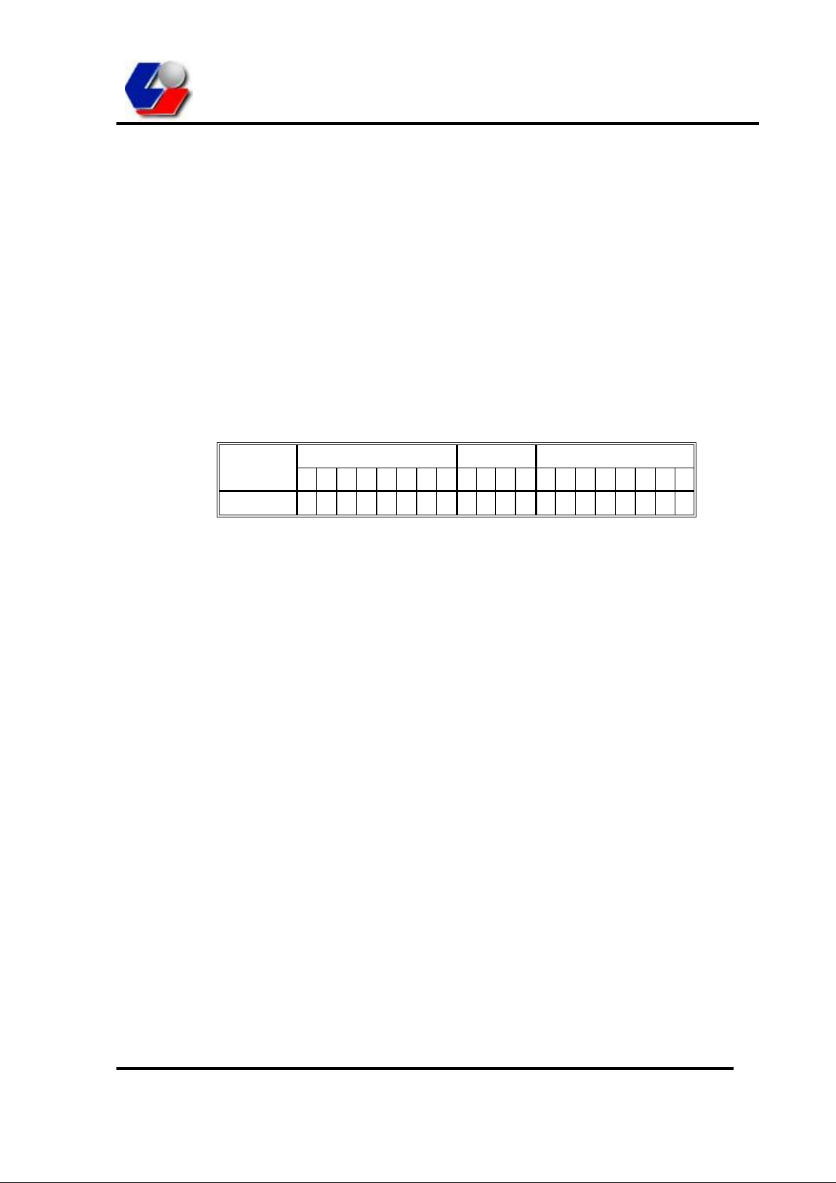
P o r t 1 P 2 P o r t 3
7 6 5 4 3 2 1 0 3 2 1 0 7 6 5 4 3 2 1 0
Pull-up
6. Customer code :
Code form ----------------- ( ) EPROM ( ) file _______________
Checksum ----------------- 00000-07FFF __________H
08000-0FFFF __________H
10000-17FFF __________H
00000-17FFF __________H
7. Operating conditions :
All the operating conditions listed below are for Syntek reference. Syntek will not guaranty on these
values. Please refer to data book or contact Syntek for the guaranty values.
Operating voltage : _____-_____ V
Operating current : _____ mA Operating frequency : _____ Hz
Sleep current :
Mode 1 : _____ µA (LCD off)
Mode 2 : _____ µA (LCD on), _____ µA (LCD off)
Customer : __________________ Salesman : __________________Date : __/__/__
 Loading...