

Page 1
STGP7NB60HD
N-CHANNEL 7A - 600V TO-220/FP
TYPE V
ST G P7NB60HD
ST G P7NB60HDFP
■ HIGHINPUT IMPEDANCE
CES
600 V
600 V
(VOLTAGEDRIVEN)
■ LOW ON-VOLTAGEDROP (V
■ LOW GATECHARGE
■ HIGHCURRENTCAPABILITY
■ VERYHIGH FREQUENCYOPERATION
■ OFFLOSSES INCLUDETAIL CURRENT
■ CO-PACKAGEDWITH TURBOSWITCH
ANTIPARALLELDIODE
DESCRIPTION
Using the latest high voltage technology based
on a patented strip layout, STMicroelectronics
has designed an advanced family of IGBTs, the
PowerMESH IGBTs, with outstanding
perfomances. The suffix ”H” identifies a family
optimized to achieve very low switching times for
high frequencyapplications(<120kHz).
V
CE(sat)
I
C
<2.8V
<2.8V7A7A
)
cesat
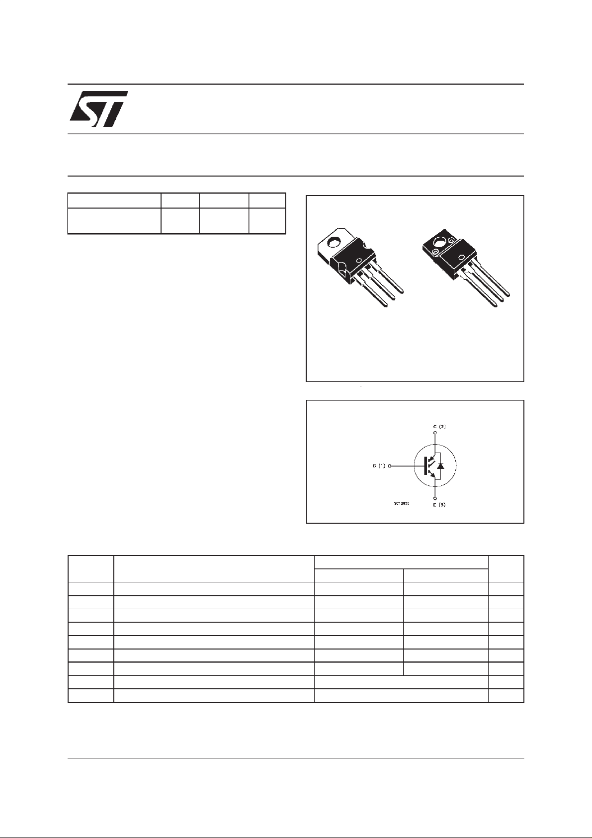
STGP7NB60HDFP
PowerMESH IGBT
3
2
1
TO-220 TO-220FP
INTERNAL SCHEMATIC DIAGRAM
3
2
1
APPLICATIONS
■ HIGHFREQUENCY MOTOR CONTROLS
■ SMPSAND PFC IN BOTH HARDSWITCH
AND RESONANTTOPOLOGIES
ABSOLUTE MAXIMUM RATINGS
Sym bol Parame t er Value Unit
STGP7NB60HD ST G P7 NB 60H DF P
V
V
I
CM
P
T
(•) Pulse widthlimited by safe operating area
June 1999
Collec t or -Emitte r Volt age (VGS = 0) 600 600 V
CES
Gate-Emitter Voltage ± 20 ± 20 V
GE
Collec t or Curr e nt (contin uous) at Tc = 25oC14 13A
I
C
Collec t or Curr e nt (contin uous) at Tc = 100oC7 6 A
I
C
(•) Collec t or Curr e nt (pulsed) 56 56 A
Total Dissipation at Tc = 25oC8035W
tot
Derat i ng Fac t or 0.64 0. 28 W/
St orage Tem p er at u re -65 to 150
stg
Max. Operat ing Junct ion Temp er at u re 150
T
j
o
C
o
C
o
C
1/9
Page 2
STGP7NB60HD/FP
THERMAL DATA
R
thj-case
R
thj-amb
R
thc-sink
Ther mal Resistanc e Junct ion-case Max 1.56 3.57
Ther mal Resistanc e Junct ion-ambient Max
Ther mal Resistanc e Case-sink Ty p
TO-220 TO- 220FP
62.5
0.5
o
C/W
o
C/W
o
C/W
ELECTRICAL CHARACTERISTICS
=25oC unless otherwise specified)
(T
j
OFF
Sym bol Parame t er Test Conditions M in. Typ. Max. U nit
V
BR(CES)
Collector-Emitter
IC=250µAVGE= 0 600 V
Break dow n Volt age
I
I
CES
GES
Collect o r cut - off
=0)
(V
GE
Gat e- Em i t t er Leakage
Current (V
CE
=0)
V
=MaxRating Tj=25oC
CE
=MaxRating Tj=125oC
V
CE
= ± 20 V VCE=0 ±100 nA
V
GE
250
2000µAµA
ON(∗)
Sym bol Parame t er Test Conditions M in. Typ. Max. U nit
V
GE(th)
Gate Th reshold
VCE=VGEIC= 250 µ A35V
Voltage
V
CE(SAT)
Collector-Emitter
Sat urat ion Volt age
VGE=15V IC=7A
=15V IC=7A Tj=125oC
V
GE
2.3
1.9
2.8 V
DYNAMIC
Sym bol Parame t er Test Conditions M in. Typ. Max. U nit
C
C
C
Q
Q
g
Q
I
CL
Forward
fs
Tr ansc on duc tance
Input Capacitanc e
ies
Out put Capacitance
oes
Reverse Transfer
res
Capacit a nc e
Tot al Gate Charge
G
Gate-Emitt er C harge
GE
Gat e- Col lect or C har ge
GC
Latc hing Curr ent V
VCE=25 V IC=7A 3.5 5 S
VCE=25V f=1MHz VGE= 0 390
45
10
VCE= 480 V IC=7A VGE=15V 42
560
68
15
730
90
20
55 nC
7.9
17.6
=480V RG=10Ω
clamp
T
= 150oC
j
28 A
V
pF
pF
pF
nC
nC
SWITCHINGON
Sym bol Parame t er Test Conditions M in. Typ. Max. U nit
(di/dt)
2/9
t
d(on)
t
r
Eon(❍)
Delay Time
Rise Time
Tur n-on Current Slope
on
Turn-on
Switching Losses
VCC= 480 V IC=7A
=15V RG=10Ω
V
GE
V
=480V IC=7A
CC
=10Ω VGE=15V
R
G
T
=125oC
j
15
48
160
185
ns
ns
A/µs
J
µ
Page 3
STGP7NB60HD/FP
ELECTRICAL CHARACTERISTICS
(continued)
SWITCHINGOFF
Sym bol Parame t er Test Conditions M in. Typ. Max. U nit
tr(v
t
E
E
tr(v
t
E
E
t
d(off
off
ts
t
d(off
off
ts
Cross-Over Time
c
Off Voltage Rise Time
)
off
)
Delay Time
t
Fall T ime
f
(**)
Turn-off Switching Loss
(❍)
Tot al Switching Loss
Cross-Over Time
c
Off Voltage Rise Time
)
off
Delay Time
)
Fall T ime
t
f
Turn-off Switching Loss
(**)
(❍)
Tot al Switching Loss
V
=480V IC=7A
CC
R
=10
Ω
=480V IC=7A
=10
Ω
= 125oC
V
R
T
GE
CC
GE
j
VGE=15V
VGE=15V
85
20
75
70
85
235
150
50
110
110
220
405
COLLECTOR-EMITTERDIODE
Sym bol Param e t er Tes t Conditions Min . Typ. Max. Unit
I
For ward Current
f
I
V
t
Q
I
rrm
(•) Pulse width limited by max. junction temperature
(
❍) Include recovery lossess on the STTA506 freewheeling diode
(∗) Pulsed: Pulse duration= 300µs, duty cycle 1.5%
(**)Losses Include Also The Tail (Jedec Standardization)
For ward Current pulsed
fm
For ward On- Voltage If=7A
f
Reverse Recovery Time
rr
Reverse Recovery Charge
rr
Reverse Recovery Current
=7A Tj= 125oC
I
f
If=7A VR=200 V
dI/dt = 100 A/µST
= 125oC
j
1.6
1.4
100
180
3.6
7
56
2.0 V
ns
ns
ns
ns
µJ
µ
ns
ns
ns
ns
µ
µ
J
J
J
A
A
V
ns
nC
A
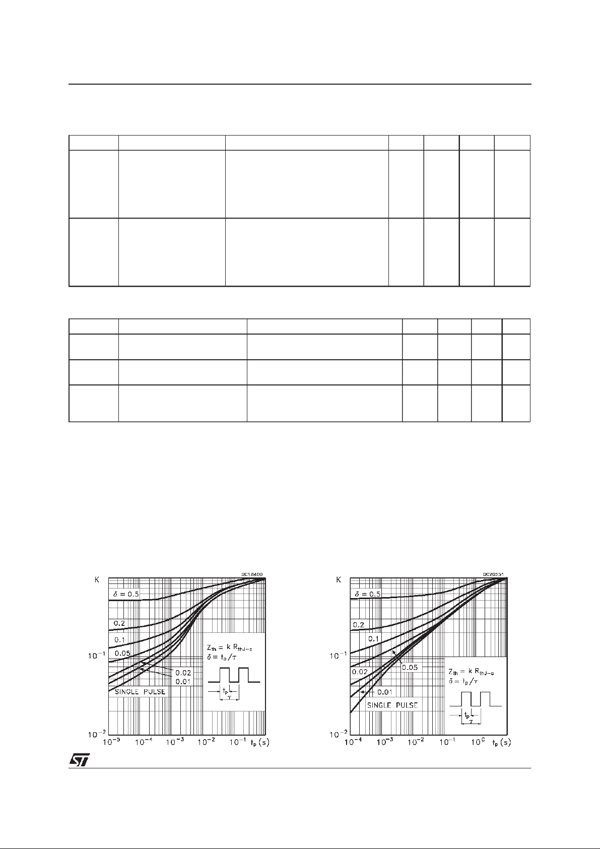
ThermalImpedeanceFor TO-220 ThermalImpedeanceFor TO-220FP
3/9
Page 4

STGP7NB60HD/FP
OutputCharacteristics
Transconductance
TransferCharacteristics
Collector-EmitterOnVoltagevs Temperature
Collector-EmitterOnVoltagevs Collector Current
4/9
Gate Thresholdvs Temperature
Page 5

STGP7NB60HD/FP
NormalizedBreakdown Voltage vs Temperature
Gate Chargevs Gate-EmitterVoltage
CapacitanceVariations
TotalSwitchingLossesvs Gate Resistance
TotalSwitchingLossesvs Temperature
TotalSwitchingLossesvs Collector Current
5/9
Page 6

STGP7NB60HD/FP
SwitchingOff SafeOperatingArea DiodeForward Voltage
Fig. 1:
Gate Charge test Circuit
Fig. 3: Switching Waveforms
Fig. 2:
TestCircuitFor Inductive LoadSwitching
6/9
Page 7

TO-220 MECHANICALDATA
STGP7NB60HD/FP
DIM.
MIN. TYP. MAX. MIN. TYP. MAX.
A 4.40 4.60 0.173 0.181
C 1.23 1.32 0.048 0.051
D 2.40 2.72 0.094 0.107
D1 1.27 0.050
E 0.49 0.70 0.019 0.027
F 0.61 0.88 0.024 0.034
F1 1.14 1.70 0.044 0.067
F2 1.14 1.70 0.044 0.067
G 4.95 5.15 0.194 0.203
G1 2.4 2.7 0.094 0.106
H2 10.0 10.40 0.393 0.409
L2 16.4 0.645
L4 13.0 14.0 0.511 0.551
L5 2.65 2.95 0.104 0.116
L6 15.25 15.75 0.600 0.620
L7 6.2 6.6 0.244 0.260
L9 3.5 3.93 0.137 0.154
DIA. 3.75 3.85 0.147 0.151
mm inch
E
A
L4
D
F2
F1
G1
H2
G
F
P011C
C
D1
L2
Dia.
L5
L7
L6
L9
7/9
Page 8

STGP7NB60HD/FP
TO-220FP MECHANICAL DATA
DIM.
MIN. TYP. MAX. MIN. TYP. MAX.
A 4.4 4.6 0.173 0.181
B 2.5 2.7 0.098 0.106
D 2.5 2.75 0.098 0.108
E 0.45 0.7 0.017 0.027
F 0.75 1 0.030 0.039
F1 1.15 1.7 0.045 0.067
F2 1.15 1.7 0.045 0.067
G 4.95 5.2 0.195 0.204
G1 2.4 2.7 0.094 0.106
H 10 10.4 0.393 0.409
L2 16 0.630
L3 28.6 30.6 1.126 1.204
L4 9.8 10.6 0.385 0.417
L6 15.9 16.4 0.626 0.645
L7 9 9.3 0.354 0.366
Ø 3 3.2 0.118 0.126
mm inch
E
A
D
B
L3
L6
L7
¯
F1
F
G1
H
G
F2
123
L2
L4
8/9
Page 9

STGP7NB60HD/FP
Information furnished is believedtobeaccurateand reliable.However, STMicroelectronics assumesno responsibility forthe consequences
of use of such information nor for any infringement of patents or other rights of third parties which may resultfrom its use. No license is
granted by implication orotherwise under any patent or patentrights of STMicroelectronics. Specificationmentioned in this publicationare
subjecttochange without notice.Thispublicationsupersedes andreplacesall information previously supplied. STMicroelectronics products
are not authorized for use as critical components in life support devicesor systems without expresswritten approval of STMicroelectronics.
The ST logo is a trademark of STMicroelectronics
1999STMicroelectronics – Printed in Italy – All Rights Reserved
STMicroelectronics GROUP OF COMPANIES
Australia - Brazil - China- Finland - France - Germany - Hong Kong - India - Italy - Japan - Malaysia - Malta - Morocco -
Singapore - Spain - Sweden - Switzerland - United Kingdom - U.S.A.
http://www.st.com
.
9/9
 Loading...