

Page 1
STGE200NB60S
N-CHANNEL 150A - 600V -ISOTOP
PowerMESH™ IGBT
TYPE
V
CES
STGE200NB60S 600 V 1.2 V
■ HIGH INPUTIMPEDANCE(VOLTAGE DRIVEN)
■ LOW ON-VOLTAGE DROP (V
■ OFF LOSSES INCLUDE TAIL CURRENT
■ LOW GATE CHARGE
■ HIGH CURRENT CAPABILITY
V
CE(sat)
(typ.)
1.3 V
cesat
I
C
150 A
200 A
)
T
C
100°C
25°C
DESCRIPTION
Using the latest h igh voltage technology based on a
patented strip layout, STMicroelectronics has
designed an advanced family of IGBTs, the
PowerMESH
™
IGBTs, with outstanding
performances. The suffix “S” identifies a family
optimized to achieve very low
V
CE(sat)
(@ max
frequency of 1KHz).
APPLICATIONS
■ LOW FREQUENCY M OTOR CONTROLS
■ ALUMINUM WELDING EQUIPMENT
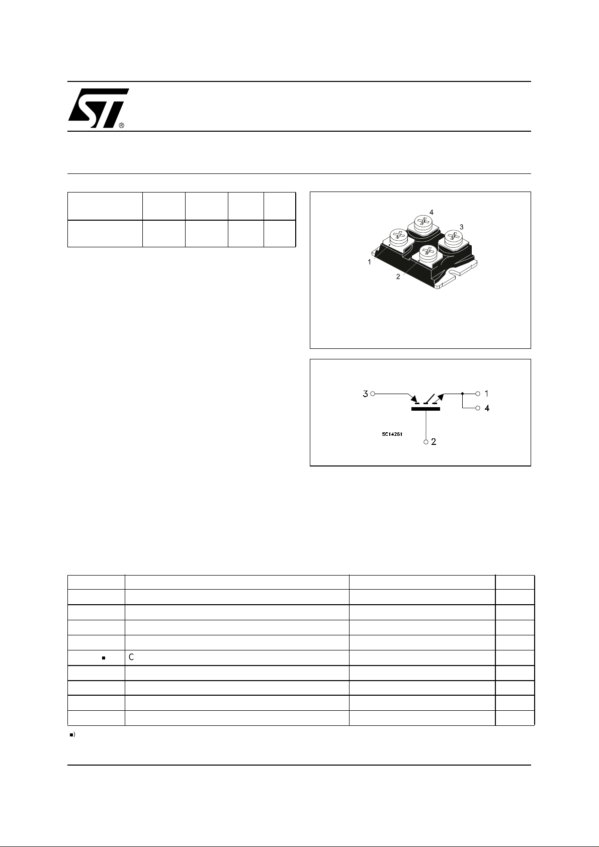
ISOTOP
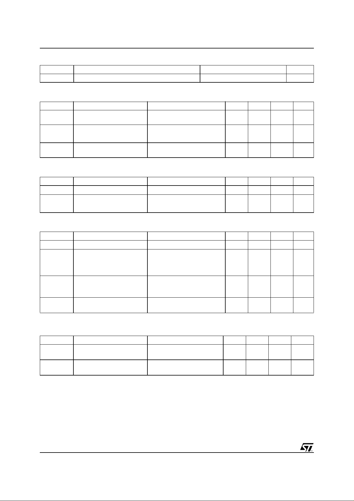
INTERNAL SCHEMATIC DIAGRAM
ABSOLUTE MAXIMUM RATINGS
Symbol Parameter Value Unit
V
CES
V
GE
I
C
I
C
ICM()
P
TOT
T
stg
T
j
() PULSE WIDTH LIMITED BY SAFE OPERATING AREA
Collector-Emitter Voltage (VGS=0)
600 V
Gate-Emitter Voltage ±20 V
Collector Current (continuous) at TC=25°C
Collector Current (continuous) at TC=100°C
200 A
150 A
Collector Current (pulsed) 400 A
Total Dissipation at TC= 25°C
600 W
Derating Factor 4.8 W/°C
Storage Temperature – 65 to 150 °C
Max. Operating Junction Temperature 150 °C
1/9June 2003
Page 2
STGE200NB60S
THERMAL DATA
Rthj-case Thermal Resistance Junction-case Max 0.208 °C/W
Rthj-amb Thermal Resistance Junction-ambient Max 30 °C/W
ELECTRICAL CHARACTERISTICS (T
= 25 °C UNLESS O THERWISE SPECIFIED)
CASE
OFF
Symbol Parameter Test Conditions Min. Typ. Max. Unit
V
BR(CES)
Collector-Emitter Breakdown
IC= 250 µA, VGE= 0 600 V
Voltage
I
CES
I
GES
Collector cut-off
=0)
(V
GE
Gate-Emitter Leakage
Current (V
CE
=0)
V
= Max Rating, TC=25°C
CE
= Max Rating, TC= 125 °C
V
CE
V
=±20V,VCE= 0 ±100 nA
GE
500 µA
5mA
ON (1)
Symbol Parameter Test Conditions Min. Typ. Max. Unit
V
GE(th)
V
CE(sat)
Gate Threshold Voltage
Collector-Emitter Saturation
Voltage
V
CE=VGE,IC
VGE=15V,IC= 100 A
=15V,IC=150 A, Tj =100°C
V
GE
= 250µA
35V
1.2 1.6 V
1.2 V
DYNAMIC
Symbol Parameter Test Conditions Min. Typ. Max. Unit
V
g
fs
C
ies
C
oes
C
res
Q
g
Q
ge
Q
gc
I
CL
Forward Transconductance
Input Capacitance
Output Capacitance
Reverse Transfer
Capacitance
Total Gate Charge
Gate-Emitter Charge
Gate-Collector Charge
Latching Current V
=15V,IC=100A
CE
=25V,f=1MHz,VGE=0
V
CE
= 480V, IC= 100 A,
V
CE
V
=15V
GE
= 480 V
clamp
Tj = 125°C , R
=10Ω
G
80 S
15600
1100
95
560
70
170
300 A
pF
pF
pF
nC
nC
nC
SWITCHING ON
Symbol Parameter Test Conditions Min. Typ. Max. Unit
t
d(on)
t
(di/dt)
Eon
Turn-on Delay Time
r
Rise Time
Turn-on Current Slope
on
Turn-on Switching Losses
=480V,IC= 100 A
V
CC
RG=2Ω,VGE=15V
VCC= 480 V,IC= 100 A RG=2Ω
VGE= 15 V,Tj = 125°C
64
112
1800
12
ELECTRICAL CHARACTERISTICS (CONTINUED)
2/9
µs
µs
A/µs
mJ
Page 3
STGE200NB60S
SWITCHING OFF
Symbol Parameter Test Conditions Min. Typ. Max. Unit
V
t
c
tr(V
off
t
d(off
t
f
E
(**)
off
E
ts
t
c
t
r(Voff
t
d(off
t
f
E
(**)
off
E
ts
Note: 1. Pulsed: Pulse duration = 300 µs, duty cycle 1.5 %.
2. Pulse width limited by max. junction temperature.
(**)Losses include Also the Tail (Jedec Standardization)
Cross-over Time
)
Off Voltage Rise Time 1.7 µs
)
Delay Time 2.4 µs
Fall Time 1.23 µs
Turn-off Switching Loss 59 mJ
Total Switching Loss 71 mJ
Cross-over Time
)
Off Voltage Rise Time 2.6 µs
)
Delay Time 2.8 µs
Fall Time 1.8 µs
Turn-off Switching Loss 92 mJ
Total Switching Loss 105 mJ
= 480 V, IC= 100 A,
cc
RGE=2Ω,VGE=15V
V
= 480 V, IC= 100 A,
cc
R
=2Ω,VGE=15V
GE
Tj = 125 °C
2.98 µs
4.52 µs
3/9
Page 4

STGE200NB60S
Thermal Impedance
Output Characteristics
Switching Off Safe Operating Area
Transfer Characteristics
Normalized Gate Threshold Voltage vs Temp. Transconductance
4/9
Page 5

STGE200NB60S
Gate-Charge vs Gate-Emitter VoltageCollector-Emitter On Voltage vs Temperature
Capacitance Variations Normalized Break-dow n Voltage vs Temp.
Total Switching losses vs TemperatureTotal Switching losses vs Gate Res istance
5/9
Page 6

STGE200NB60S
Collector-Emitter on Voltage vs CurrentTotal Switching l osses vs Ic
6/9
Page 7

STGE200NB60S
Fig. 2: Test Circuit For Induct ive Load SwitchingFig. 1: Gate Charge test Circuit
7/9
Page 8

STGE200NB60S
ISOTOP MECHANICAL DATA
DIM.
MIN. TYP. MAX. MIN. TYP. MAX.
A 11.8 12.2 0.466 0.480
B 8.9 9.1 0.350 0.358
C 1.95 2.05 0.076 0.080
D 0.75 0.85 0.029 0.033
E 12.6 12.8 0.496 0.503
F 25.15 25.5 0.990 1.003
G 31.5 31.7 1.240 1.248
H4 0.157
J 4.1 4.3 0.161 0.169
K 14.9 15.1 0.586 0.594
L 30.1 30.3 1.185 1.193
M 37.8 38.2 1.488 1.503
N4 0.157
O 7.8 8.2 0.307 0.322
mm inch
G
A
8/9
N
O
B
D
E
F
H
J
C
K
L
M
Page 9

STGE200NB60S
Information furnished is believed to be accurate and reliable. However, STMicroelectronics assumes no responsibility for the
consequences of u se of such inf ormat ion nor for any in fring ement of p aten ts or othe r ri ghts of th ird p arties whic h may resul t f rom
its use. No license is granted by implication or otherwise under any patent or patent rights of STMicroelectronics. Specifications
mentioned in this publication are subject to change without notice. This publication supersedes and replaces all information
previously supplied. STMicroelectronics products are not authorized for use as critical components in life support devices or
systems without express written approval of STMicroelectronics.
Australia - Brazil - Canada - China - Finland - France - Germany - Hong Kong - India - Israel - Italy - Japan - Malaysia - Malta - Morocco
© The ST logo is a registered trademark of STMicroelectronics
© 2003 STMicroelectronics - Printed in Italy - All Rights Reserved
Singapore - Spain - Sweden - Switzerland - United Kingdom - United States.
STMicroelectronics GROUP OF COMPANIES
© http://www.st.com
9/9
 Loading...