

Page 1
查询STGD7NC60H供应商
STGP7NC60H - STGD7NC60H
N-CHANNEL 14A - 600V TO-220/DPAK
Very Fast PowerMESH™ IGBT
Table 1: Ge neral Features
TYPE V
STGP7NC60H
STGD7NC60HT4
■ LOWER ON-VOLTAGE DROP (V
■ OFF LOSSES INCLUDE TAIL CURRENT
■ LOWER C
■ HIGH FREQUENCY OPERATION UP TO 70
RES/CIES
CESVCE(sat)
600 V
600 V
RATIO
(Max)
@25°C
< 2.5 V
< 2.5 V
cesat
I
C
@100°C
14 A
14 A
)
KHz
■ NEW GENERATION PRODUCTS WITH
TIGHTER PARAMETER DISTRIBUTION
DESCRIPTION
Using the latest high voltage technology based on
a patented strip layout, STMicroelectronics has
designed an advanced family of IGBTs, the PowerMESH
™
IGBTs, with outstanding performances.
The suffix "H" identifies a family optimized for high
frequency applications in order to achieve very
high switching performances (reduced tfall) mantaining a low voltage drop.
APPLICATIONS
■ HIGH FREQUENCY INVERTERS
■ SMPS AND PFC IN BOTH HARD SWITCH
AND RESONANT TOPOLOGIES
■ MOTOR DRIVERS
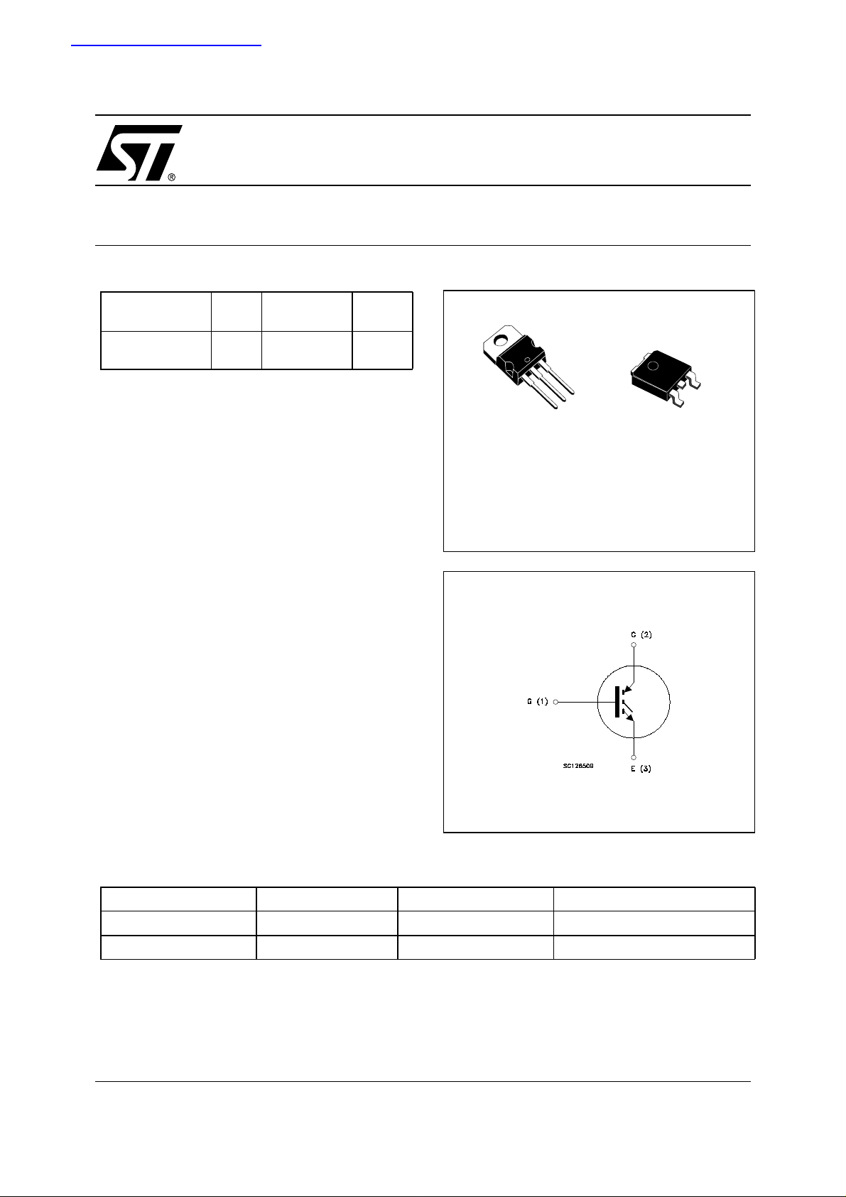
Figure 1: Package
3
2
1
TO-220
DPAK
Weight for TO-220: 1.92gr ± 0.01
Weight for DPAK: 0.38gr ± 0.01
Figure 2: Internal Schematic Diagram
3
1
Table 2: Order Code
PART NUMBER MARKING PACKAGE PACKAGING
STGP7NC60H GP7NC60H TO-220 TUBE
STGD7NC60HT4 D7NC60H DPAK TAPE & REEL
Rev. 2
1/12June 2005
Page 2
STGP7NC60H - STGD7NC 60H
Table 3: Absolute Maximum ratings
Symbol Parameter Value Unit
TO-220 DPAK
V
CES
V
ECR
V
GE
I
C
I
C
I
()
CM
P
TOT
T
stg
T
j
() Pulse width limite d by max. juncti on t em perature.
Table 4: Thermal Data
Rthj-case Thermal Resistance Junction-case TO-220 1.56
Rthj-amb Thermal Resistance Junction-ambient TO-220 62.5
T
L
Collector-Emitter Voltage (VGS = 0)
600 V
Emitter-Collector Voltage 20 V
Gate-Emitter Voltage ±20 V
Collector Current (continuous) at TC = 25°C (#)
Collector Current (continuous) at TC = 100°C (#)
25 A
14 A
Collector Current (pulsed) 50 A
Total Dissipation at TC = 25°C
80 70 W
Derating Factor 0.64 0.56 W/°C
Storage Temperature
Operating Junction Temperature
– 55 to 150 °C
Min. Typ. Max.
DPAK 1.78
DPAK 100
Maximum Lead Temperature for Soldering
Purpose (1.6 mm from case, for 10 sec.)
TO-220 300
DPAK 275
°C/W
°C/W
°C
ELECTRICAL CHARACTERISTICS (T
=25°C UNLESS OTHERWISE SPECIFIED)
CASE
Table 5: Main Parameters
Symbol Parameter Test Conditions Min. Typ. Max. Unit
V
BR(CES)
Collector-Emitter
Breakdown Voltage
I
CES
I
GES
V
GE(th)
V
CE(sat)
Collector cut-off Current
= 0)
(V
GE
Gate-Emitter Leakage
Current (V
CE
= 0)
Gate Threshold Voltage
Collector-Emitter
Saturation Voltage
(#) Calculated according to the iterative formula:
T
–
ICTC()
--------------------------------------------------------------------------------------------------
=
R
THJ C–
JMAXTC
V
CESAT MAX()TCIC
IC = 1 mA, VGE = 0 600 V
V
= Max Rating, TC= 25 °C
CE
= Max Rating, TC= 125 °C
V
CE
V
= ± 20V , VCE = 0 ±100 nA
GE
V
= VGE, IC = 250 µA
CE
VGE = 15V, IC = 7 A
VGE = 15V, IC = 7 A, Tc= 125°C
,()×
3.75 5.75 V
1.85
1.7
10
1
2.5 V
µA
mA
V
2/12
Page 3
STGP7NC60H - STGD 7NC60H
ELECTRICAL CHARACTERISTICS (CONTINUED)
Table 6: Dynamic
Symbol Parameter Test Conditions Min. Typ. Max. Unit
(1)
g
fs
C
ies
C
oes
C
res
Forward Transconductance
Input Capacitance
Output Capacitance 81 pF
Reverse Transfer
Capacitance
Q
g
Q
ge
Q
gc
I
CL
Total Gate Charge
Gate-Emitter Charge
Gate-Collector Charge
Turn-Off SOA Minimum
Current
(1) Pulsed: Pulse durat ion= 300 µs, duty cycle 1.5%
Table 7: Switching On
Symbol Parameter Test Conditions Min. Typ. Max. Unit
t
d(on)
t
(di/dt)
t
d(on)
t
(di/dt)
r
r
Turn-on Delay Time
Current Rise Time
Turn-on Current Slope
on
Turn-on Delay Time
Current Rise Time
Turn-on Current Slope
on
VCE = 15 V , IC= 7 A 4.30 S
V
= 25 V, f= 1 MHz, VGE = 0
CE
720 pF
17 pF
= 390 V, IC = 7 A,
V
CE
VGE = 15 V
(see Figure 21)
V
= 480 V , Tj = 150°C
clamp
R
= 10 Ω, VGE = 15 V
G
VCC = 390 V, IC = 7 A
R
=10 Ω, VGE= 15V, Tj= 25°C
G
(see Figure 18)
VCC = 390 V, IC = 7 A
RG=10 Ω, VGE= 15V , Tj= 125°C
(see Figure 19)
50 A
35
7
16
18.5
8.5
1060
18.5
7
1000
48 nC
nC
nC
ns
ns
A/µs
ns
ns
A/µs
Table 8: Switching Off
Symbol Paramet er Test Conditions Min. Typ. Max. Unit
t
r(Voff
t
d(off
t
r(Voff
t
d(off
)
Off Voltage Rise Time
)
Turn-off Delay Time 72 ns
t
f
t
f
Current Fall Time 60 ns
)
Off Voltage Rise Time
)
Turn-off Delay Time 116 ns
Current Fall Time 105 ns
Vcc = 390 V, IC = 7 A,
R
= 10 Ω , VGE = 15 V
G
TJ = 25 °C
(see Figure 19)
Vcc = 390 V, IC = 7 A,
R
= 10 Ω , VGE = 15 V
G
Tj = 125 °C
(see Figure 19)
27 ns
56 ns
Table 9: Switching Energy
Symbol Parameter Test Conditions Min. Typ. Max Unit
Eon (2)
E
off
E
ts
Eon (2)
E
off
E
ts
2) Eon is the turn-on losses when a typical diode is used in the test circuit in figure 2. If the IGBT is offered in a package with a co-pack diode,
the co-pack diode is used as external di ode. IGBTs & DIODE are at the same temperat ure (25°C and 125 °C)
(3)Turn-off losse s include also the tail of the coll ector current .
Turn-on Switching Losses
Turn-off Switching Loss
(3)
Total Switching Loss
Turn-on Switching Losses
Turn-off Switching Loss
(3)
Total Switching Loss
= 390 V, IC = 7 A
V
CC
R
= 10 Ω, VGE= 15V, Tj= 25°C
G
(see Figure 19)
= 390 V, IC = 7 A
V
CC
RG= 10 Ω, VGE= 15V, Tj= 125°C
(see Figure 19)
95
115
210
140
215
355
125
150
275
µJ
µJ
µJ
µJ
µJ
µJ
3/12
Page 4
STGP7NC60H - STGD7NC 60H
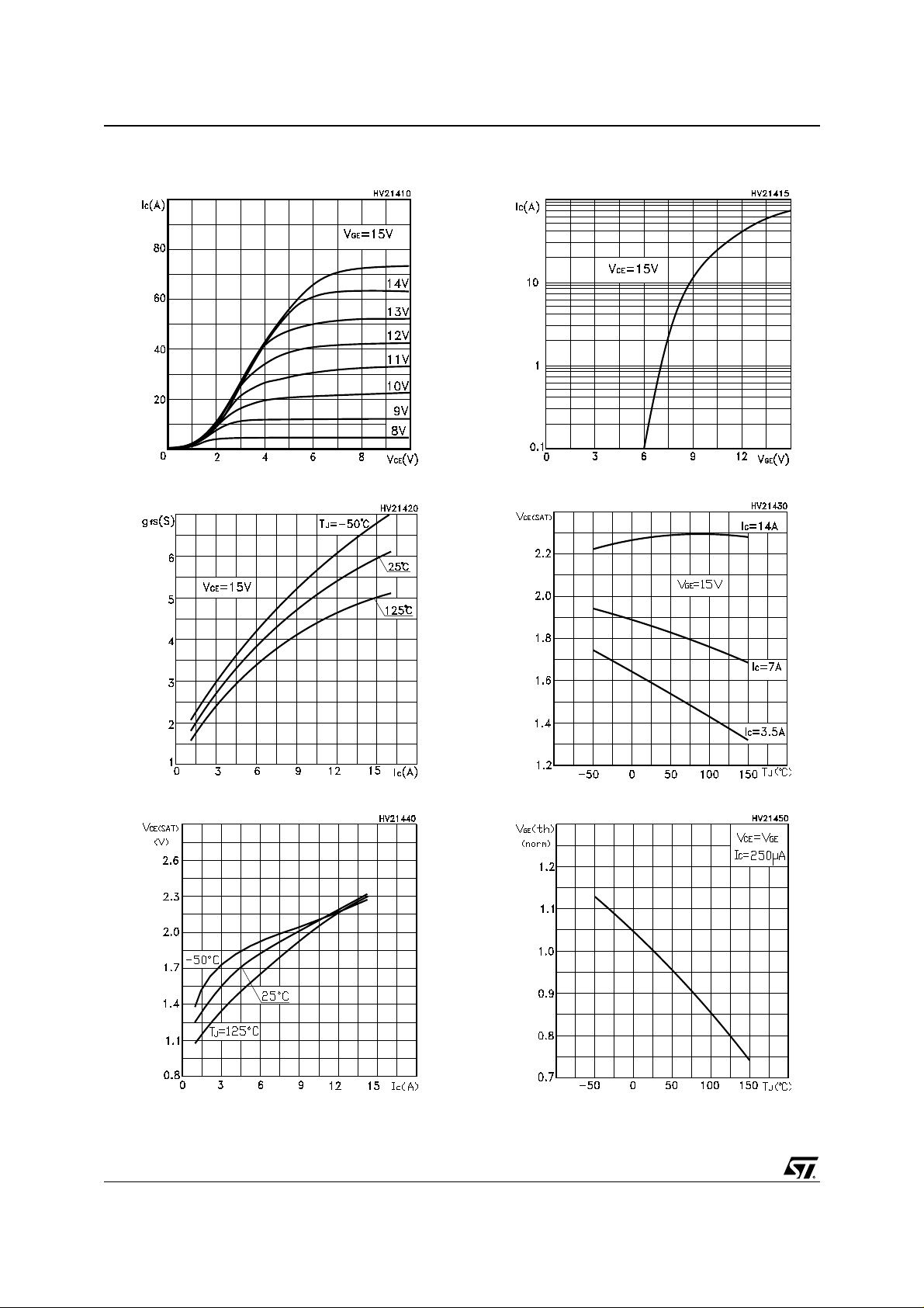
Figure 3: Output Characteristics
Figure 4: Transconductance
Figure 6: Transfer Characteristics
Figure 7: Collector-Emitter On Voltage vs Temperature
Figure 5: Collector-Emitter On Voltage vs Collector Curr e nt
4/12
Figure 8: Normalized Gate Threshold vs Temperature
Page 5

STGP7NC60H - STGD 7NC60H
Figure 9: Normalized Breakdown Voltage vs
Temperature
Figure 10: Capacitance Variations
Figure 12: Gate Charge vs G ate-Emitter Voltage
Figure 13: Total Switching Lo sses vs Temp erature
Figure 11: Total Switching Losses vs Gate Resistance
Figure 14: Total Switching Losses vs Collector
Current
5/12
Page 6

STGP7NC60H - STGD7NC 60H
Figure 15: Thermal Impedan ce for TO-220
Figure 16: Thermal Impedance for DPAK
Figure 17: Turn-Of f S OA
Figure 18: Ic v s Fr equenc y
For a fast IGBT suitable for high frequency applications, the typical collector current vs. maximum
operating frequency curve is reported. That frequency is defined as follows:
f
= (PD - PC) / (EON + E
MAX
OFF
)
1) The maximum power dissipation is limited by
maximum junction to case thermal resistance:
P
= ∆T / R
D
THJ-C
considering ∆T = TJ - TC = 125 °C- 75 °C = 50°C
2) The conduction losses are:
P
= IC * V
C
with 50% of duty cycle, V
CE(SAT)
* δ
typical value
CESAT
@125°C.
3) Power dissipation during ON & OFF commutations is due to the switching frequency:
P
= (EON + E
SW
OFF
) * freq.
4) Typical values @ 125°C for switching losse s are
used (test conditions: V
= 3.3 Ohm). Fu rthermore, diode recovery en-
R
G
ergy is included in the E
tail of the collector current is included in the E
= 390V, VGE = 15V,
CE
(see note 2), while the
ON
OFF
measurements (see note 3).
6/12
Page 7

STGP7NC60H - STGD 7NC60H
Figure 19: Test Circuit for Inductive Load
Swit c hing
Figure 20: Switching Waveforms
Figure 21: Gate Charge Test Circuit
7/12
Page 8

STGP7NC60H - STGD7NC 60H
TO-220 MECHANICAL DATA
DIM.
A 4.40 4.60 0.173 0.181
b 0.61 0.88 0.024 0.034
b1 1.15 1.70 0.045 0.066
c 0.49 0.70 0.019 0.027
D 15.25 15.75 0.60 0.620
E 10 10.40 0.393 0.409
e 2.40 2.70 0.094 0.106
e1 4.95 5.15 0.194 0.202
F 1.23 1.32 0.048 0.052
H1 6.20 6.60 0.244 0.256
J1 2.40 2.72 0.094 0.107
L 13 14 0.511 0.551
L1 3.50 3.93 0.137 0.154
L20 16.40 0.645
L30 28.90 1.137
øP
Q 2.65 2.95 0.104 0.116
MIN. TYP MAX. MIN. TYP. MAX.
3.75 3.85 0.147 0.151
mm. inch
8/12
Page 9

STGP7NC60H - STGD 7NC60H
TO-252 (DPAK) MECHANICAL DATA
DIM.
A 2.20 2.40 0.087 0.094
A1 0.90 1.10 0.035 0.043
A2 0.03 0.23 0.001 0.009
B 0.64 0.90 0.025 0.035
B2 5.20 5.40 0.204 0.213
C 0.45 0.60 0.018 0.024
C2 0.48 0.60 0.019 0.024
D 6.00 6.20 0.236 0.244
E 6.40 6.60 0.252 0.260
G 4.40 4.60 0.173 0.181
H 9.35 10.10 0.368 0.398
L2 0.8 0.031
L4 0.60 1.00 0.024 0.039
V2 0
MIN. TYP. MAX. MIN. TYP. MAX.
o
mm inch
o
8
o
0
o
0
P032P_B
9/12
Page 10

STGP7NC60H - STGD7NC 60H
DPAK FOOTPRINT
All dimensions are in millimeters
TAPE AND REEL SHIPMENT
REEL MECHANICAL DATA
DIM.
A 330 12.992
B 1.5 0.059
C 12.8 13.2 0.504 0.520
D 20.2 0.795
G 16.4 18.4 0.645 0.724
N 50 1.968
T 22.4 0.881
mm inch
MIN. MAX. MIN. MAX.
TAPE MECHANICAL DATA
DIM.
A0 6.8 7 0.267 0.275
B0 10.4 10.6 0.409 0.417
B1 12.1 0.476
D 1.5 1.6 0.059 0.063
D1 1.5 0.059
E 1.65 1.85 0.065 0.073
F 7.4 7.6 0.291 0.299
K0 2.55 2.75 0.100 0.108
P0 3.9 4.1 0.153 0.161
P1 7.9 8.1 0.311 0.319
P2 1.9 2.1 0.075 0.082
R 40 1.574
W 15.7 16.3 0.618 0.641
mm inch
MIN. MAX. MIN. MAX.
BASE QTY BULK QTY
2500 2500
10/12
Page 11

Table 10: Revision History
Date Revision D escrip tion of Change s
20-Aug-2004 1 New datasheet
09-Jun-2005 2 Modified title
STGP7NC60H - STGD 7NC60H
11/12
Page 12

STGP7NC60H - STGD7NC 60H
Information furnished is believed to be accurate and reliable. However, STMicroelectronics assumes no responsibility for the consequences
of use of such information nor for any infringement of patents or other rights of third parties which may result from its use. No license is granted
by implic ati o n or ot h er wis e und er an y pat ent or pa te nt r igh ts of STMi cr oe l ect ro ni cs . Sp ec if i cat i on s ment i o ned i n th is p ub li c ati on ar e s ubj ec t
to change without notice. This publication supersedes and replaces all information previously sup plied. STMicroelectronics products are not
authorized for use as critical components in life support devices or systems without express written approval of STMicroelectronics.
The ST logo is a registered trademark of STMicroelectronics
All other names are the property of their respective owners
© 2005 STMicroelectronics - All Rights Reserved
STMicroelectronics group of companies
Australia - Belgium - Brazil - Canada - China - Czech Republic - Finland - France - Germany - Hong Kong - India - Israel - Italy - Japan -
Malaysia - Malta - Morocco - Singapore - Spain - Sweden - Switzerland - United Kingdom - United States of America
12/12
 Loading...