

Page 1
®
STGD7NB60S
N-CHANNEL 7A - 600V DPAK
Power MESH IGBT
TYPE V
STGD7NB60S 600 V < 1.6 V 7 A
■
HIGH INPUT IMPEDANCE
CES
V
CE(sat)
I
C
(VOLTAGE DRIVEN)
■
VERY LOW ON-VOLTAGE DROP (V
■
HIGH CURRENT CAPABILITY
■
OFF LOSSES INCLUDE TAIL CURRENT
■
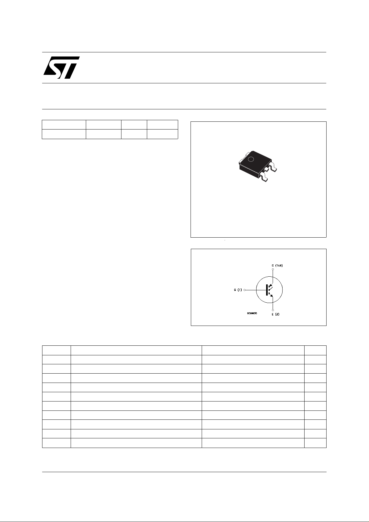
SURFACE-MOU NTING DPAK (TO-252)
cesat
)
POWER PACKAGE IN TA P E & R E EL
(SUFFIX "T4")
DESCRIPTION
Using the latest high voltage technology based
on a patented strip layout, STMicroelectronics
has designed an advanced family of IGBTs, the
PowerMESH IGBTs, with outstanding
perfomances. The suffix "S" identifies a family
optimized to achieve minimum on-voltage drop
for low frequency applications (<1kHz).
APPLICATIONS
■
LIGHT DIMMER
■
STATIC RELAYS
■
MOTOR CONTROL
3
1
DPAK
TO-252
(Suffix "T4")
INTERNAL SCHEMATIC DIAGRAM
ABSOLUTE MAXIMUM RATINGS
Symbol Parameter Value Unit
V
V
V
I
CM
P
T
(•) Pulse width limited by safe operating area
November 1999
Collector-Emitter Voltage (VGS = 0) 600 V
CES
Reverse Battery Protection 20 V
ECR
Gate-Emitter Voltage ± 20 V
GE
I
Collector Current (continuous) at Tc = 25 oC15A
C
I
Collector Current (continuous) at Tc = 100 oC7A
C
(•) Collector Current (pulsed) 60 A
Total Dissipation at Tc = 25 oC55W
tot
Derating Factor 0.44 W/
Storage Temperature -65 to 150
stg
T
Max. Operating Junction Temperature 150
j
o
C
o
C
o
C
1/8
Page 2
STGD7NB60S
THERMAL DATA
R
thj-case
R
thj-amb
R
thc-sink
Thermal Resistance Junction-case Max
Thermal Resistance Junction-ambient Max
Thermal Resistance Case-sink Typ
2.27
100
1.5
o
C/W
o
C/W
o
C/W
ELECTRICAL CHARACTERISTICS
= 25 oC unless otherwise specified)
(T
j
OFF
Symbol Parameter Test Conditions Min. Typ. Max. Unit
V
BR(CES)
Collector-Emitter
IC = 250 µA V
= 0 600 V
GE
Breakdown Voltage
V
BR(ECR)
Emitter-Collector
IC = 1 mA V
= 0 20 V
GE
Breakdown Voltage
I
I
CES
GES
Collector cut-off
(V
= 0)
GE
Gate-Emitter Leakage
Current (V
CE
= 0)
= Max Rating Tj = 25 oC
V
CE
V
= Max Rating Tj = 125 oC
CE
= ± 20 V VCE = 0 ± 100 nA
V
GE
10
100
ON (∗)
Symbol Parameter Test Conditions Min. Typ. Max. Unit
V
GE(th)
Gate Threshold
V
= VGE IC = 250 µA 2.5 5 V
CE
Voltage
V
CE(SAT)
Collector-Emitter
Saturation Voltage
VGE = 15 V IC = 3 A
V
= 15 V IC = 7 A
GE
V
= 15 V IC = 7 A Tj = 125 oC
GE
1
1.2
1.1
1.4
1.6
DYNAMIC
Symbol Parameter Test Conditions Min. Typ. Max. Unit
g
C
C
C
Q
I
CL
Forward
fs
VCE =25 V IC = 7 A 4 S
Transconductance
Input Capacitance
ies
Output Capacitance
oes
Reverse Transfer
res
V
= 25 V f = 1 MHz V
CE
= 0 610
GE
65
12
Capacitance
Gate Charge VCE = 400 V IC = 7 A VGE = 15 V 33 nC
G
Latching Current V
= 480 V RG=1kΩ
clamp
T
= 150 oC
j
15 A
780
85
15
µA
µA
V
V
V
pF
pF
pF
SWITCHING ON
Symbol Parameter Test Conditions Min. Typ. Max. Unit
0.7
0.46
8
0.4
(di/dt)
2/8
t
d(on)
E
Delay Time
Rise Time
t
r
Turn-on Current Slope
on
Turn-on
on
Switching Losses
VCC = 480 V IC = 7 A
V
= 15 V RG = 1 KΩ
GE
V
= 480 V IC = 7 A
CC
R
= 1 KΩ VGE = 15 V
G
T
= 125 oC
j
µs
µs
A/µs
mJ
Page 3
STGD7NB60S
ELECTRICAL CHARACTERISTICS (continued)
SWITCHING OFF
Symbol Parameter Test Conditions Min. Typ. Max. Unit
V
t
tr(v
E
off
t
tr(v
E
off
(•) Pulse width limited by safe operating area
(∗) Pulsed: Pulse duration = 300 µs, duty cycle 1.5 %
(**)Losses Include Also The Tail (Jedec Standardi zat io n)
Cross-Over Time
c
Off Voltage Rise Time
)
off
Fall Time
t
f
Turn-off Switching Loss
(**)
Cross-Over Time
c
Off Voltage Rise Time
)
off
Fall Time
t
f
Turn-off Switching Loss
(**)
= 480 V IC = 7 A
CC
R
= 100 Ω VGE = 15 V
GE
V
= 480 V IC = 7 A
CC
R
= 100 Ω VGE = 15 V
GE
T
= 125 oC
j
2.2
1.2
1.2
3.5
3.8
1.2
1.9
5.3
µ
µ
µ
mJ
µ
µ
µ
mJ
s
s
s
s
s
s
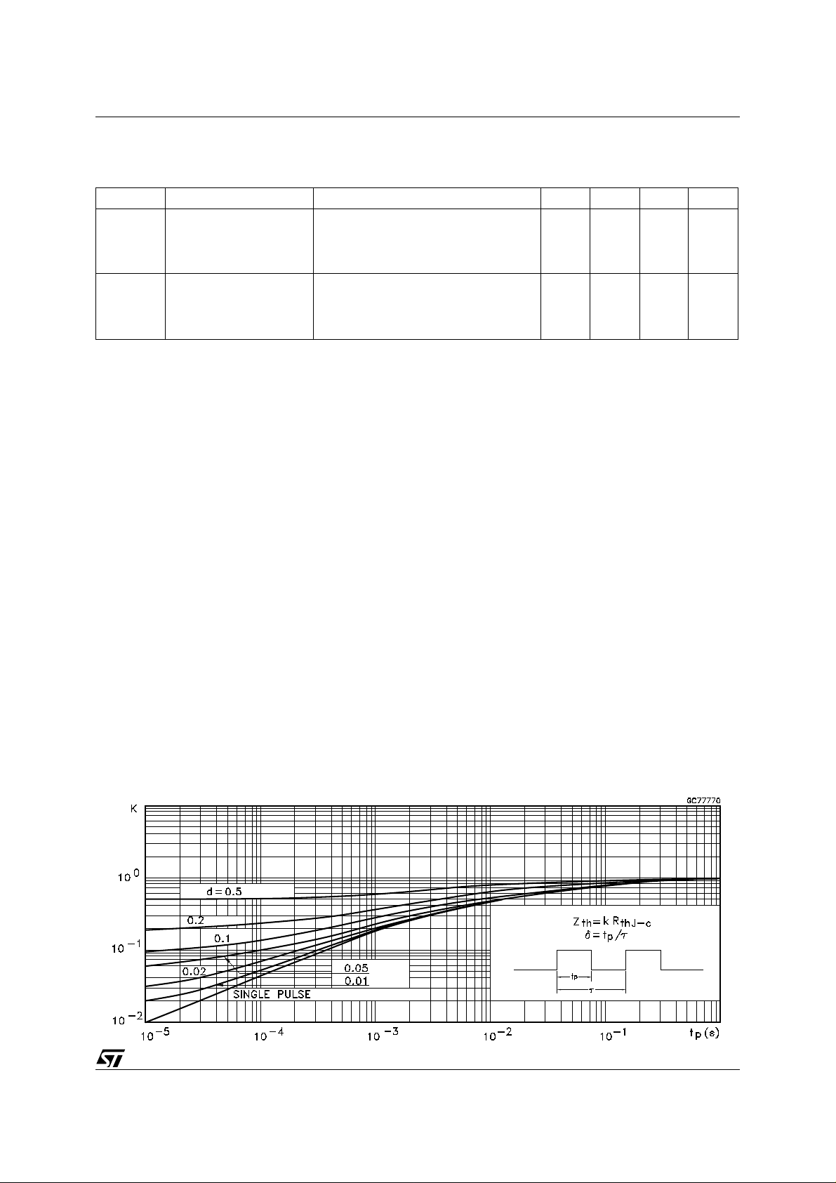
Thermal Impedance
3/8
Page 4

STGD7NB60S
Output Characteristics
Transconductance
Transfer Characteristics
Collector-Emitter On Voltage vs Temperature
Collector-Emitter On Voltage vs Collector Current
4/8
Gate Threshold vs Temperature
Page 5

STGD7NB60S
Normalized Breakdown Voltage vs Temperature
Gate Charge vs Gate-Emitter Voltage
Capacitance Variations
Off Losses vs Gate Resistance
Off Losses vs Temperature
Off Losses vs Collector Current
5/8
Page 6

STGD7NB60S
Switching Off Safe Operatin Area
Fig. 1: Gate Charge test Circuit
Fig. 3: Switching Waveforms
Fig. 2: Test Circuit For Inductive Load Switching
6/8
Page 7

TO-252 (DPAK) MECHANICAL DATA
STGD7NB60S
DIM.
mm inch
MIN. TYP. MAX. MIN. TYP. MAX.
A 2.2 2.4 0.086 0.094
A1 0.9 1.1 0.035 0.043
A2 0.03 0.23 0.001 0.009
B 0.64 0.9 0.025 0.035
B2 5.2 5.4 0.204 0.212
C 0.45 0.6 0.017 0.023
C2 0.48 0.6 0.019 0.023
D 6 6.2 0.236 0.244
E 6.4 6.6 0.252 0.260
G 4.4 4.6 0.173 0.181
H 9.35 10.1 0.368 0.397
L2 0.8 0.031
L4 0.6 1 0.023 0.039
A
C2
L2
E
B2
==
H
DETAIL "A"
D
==
C
B
2
1 3
L4
A1
G
==
A2
DETAIL "A"
0068772-B
7/8
Page 8

STGD7NB60S
Information f urnished i s believed t o be accurate an d reliabl e. How ever, STMicroelect ronics assu mes no responsib ility fo r the consequen ces
of use of such information nor for any infringement of patents or other rights of third parties which may result from its use. No license is
granted by implication or otherwise under any patent or patent rights of STMicroelectronics. Specification mentioned in this publication are
subject to chan ge w ithout notice. This publicatio n su persedes a nd r eplaces al l inf ormati on previ ously suppl ied. STMicroelect ron ics produ cts
are not auth ori zed f or use as critical components i n life sup port devices or systems witho ut express written approval of STMicroelectr o nics.
The ST logo is a trademark of STMicroelectronics
© 1999 STMicroelectroni cs – Printed i n It aly – All Rights Reserved
STMicroele ct ronics GROUP OF COMPANIES
Australia - Brazil - Chi na - Finland - France - Germ any - Hong Kong - India - Italy - Japan - Malaysia - Malta - Morocco -
8/8
Singapore - Spain - Sweden - Switzerland - United Kingdom - U.S.A.
http://www.st.com
.
 Loading...