

Page 1
STP80NF75L
STB80NF75L STB80NF75L-1
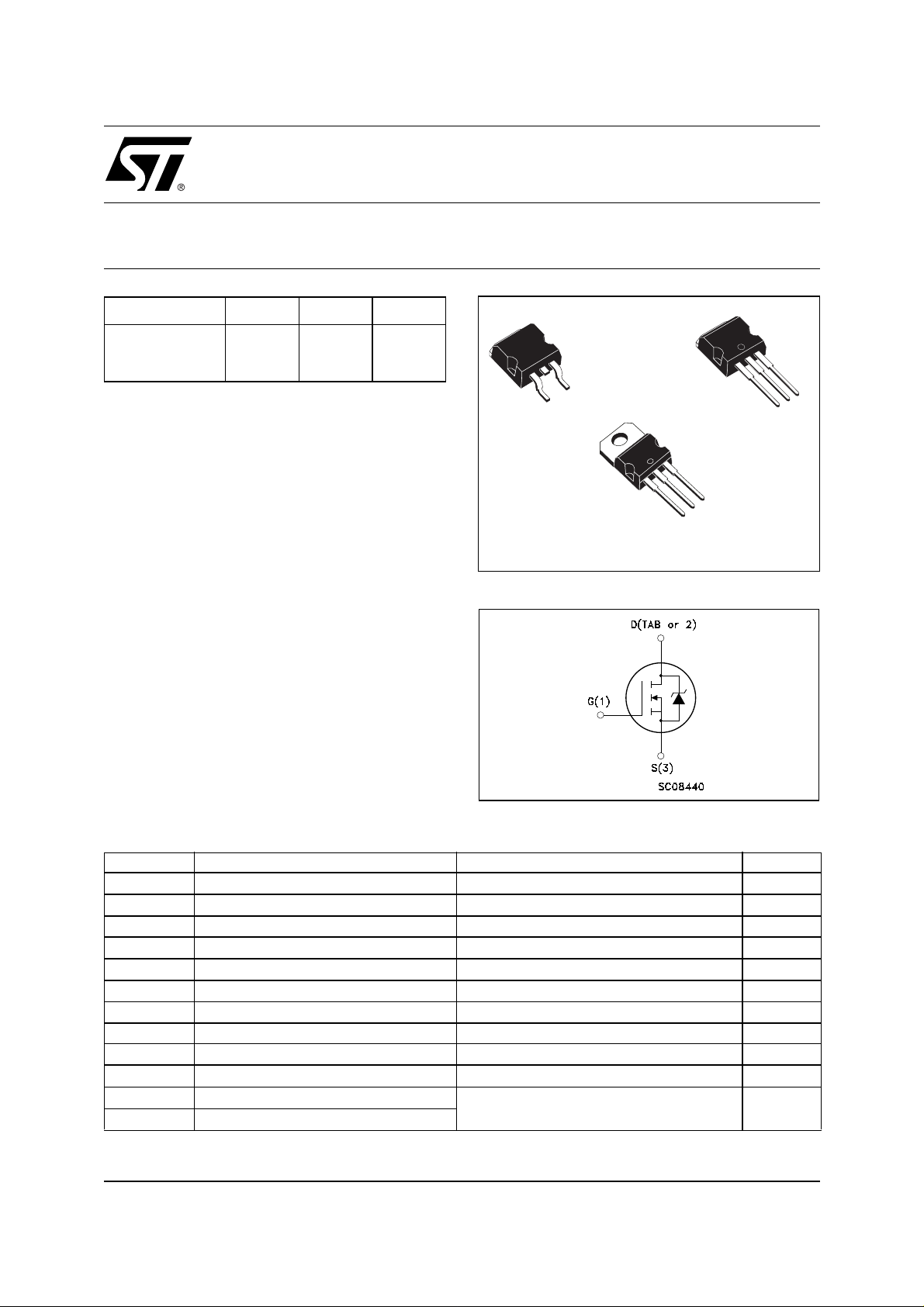
N-CHANNEL 75V - 0.008 Ω - 80A TO-220/D2PAK/I2PAK
STripFET™ II POWER MOSFET
TYPE
STP80NF75L
STB80NF75L
STB80NF75L-1
■ TYPICAL R
■ EXCEPTIONA L dv/d t CAPABILITY
■ 100% AVALANCHE TESTED
■ LOW THRESHOLD DRIVE
V
DSS
75 V
75 V
75 V
(on) = 0.008 Ω
DS
R
DS(on)
<0.01
<0.01
<0.01
I
D
80 A
Ω
80 A
Ω
80 A
Ω
DESCRIPTION
This Power MOSFET is the latest dev elo pment of
STMicroelectronis unique "Single Feature Size™"
strip-based process. The resulting transistor
shows extremely high packing density for low onresistance, rugged avalanche characteristics and
less critical alignment steps therefore a remarkable manufacturing reproducibility.
APPLICATIONS
■ HIGH CURRENT, HIGH SWITCHING SPEED
■ MOTOR CONTROL, AUDIO AMPLIFIERS
■ DC-DC & DC-AC CONVERTERS
■ SOLENOID AND RELAY DRIVERS
3
1
D2PAK
TO-263
3
2
1
TO-220
INTERNAL SCHEMATIC DIAGRAM
2
PAK
I
TO-262
3
2
1
ABSOLUTE MAXIMUM RATINGS
Symbol Parameter Value Unit
V
DS
V
DGR
V
GS
(
I
•)
D
I
D
(
I
••)
DM
P
tot
dv/dt
E
AS
T
stg
T
j
(•)Current Limited by Package
(
Pulse wi dth limited by safe operating ar ea.
••)
.
Drain-source Voltage (VGS = 0)
Drain-gate Voltage (RGS = 20 kΩ)
75 V
75 V
Gate- source Voltage ± 16 V
Drain Current (continuos) at TC = 25°C
Drain Current (continuos) at TC = 100°C
80 A
80 A
Drain Current (pulsed) 320 A
Total Dissipation at TC = 25°C
300 W
Derating Factor 2 W/°C
(1)
Peak Diode Recovery voltage slope 12 V/ns
(2)
Single Pulse Avalanche Energy 930 mJ
Storage Temperature
Max. Operating Junction Temperature
≤80A, di/dt ≤960A/ µ s , VDD ≤ V
(1) I
SD
(2) Starting Tj = 25 oC, ID = 40A, VDD= 40V
-55 to 175 °C
(BR)DSS
, Tj ≤ T
JMAX
1/11November 2001
Page 2
STB80NF75L/-1/ STP80NF75L
THERMA L D ATA
Rthj-case
Rthj-amb
T
Thermal Resistance Junction-case
Thermal Resistance Junction-ambient
Maximum Lead Temperature For Soldering Purpose
l
Max
Max
Typ
0.5
62.5
300
°C/W
°C/W
°C
ELECTRICAL CHARACTERISTICS (T
= 25 °C unless otherwise specified)
case
OFF
Symbol Parameter Test Conditions Min. Typ. Max. Unit
I
= 250 µA, VGS = 0
D
V
= Max Rating
DS
V
= Max Rating TC = 125°C
DS
V
= ± 16V
GS
75 V
1
10
±100 nA
ON
V
(BR)DSS
I
DSS
I
GSS
(*)
Drain-source
Breakdown Voltage
Zero Gate Voltage
Drain Current (V
GS
Gate-body Leakage
Current (V
DS
= 0)
= 0)
Symbol Parameter Test Conditions Min. Typ. Max. Unit
V
V
GS(th)
R
DS(on)
Gate Threshold Voltage
Static Drain-source On
Resistance
= VGS I
DS
= 5 V ID = 40 A
V
GS
V
= 10 V ID = 40 A
GS
= 250 µA
D
1 1.6 2.5 V
0.01
0.008
0.013
0.010
DYNAMIC
Symbol Parameter Test Conditions Min. Typ. Max. Unit
(*)
g
fs
C
iss
C
oss
C
rss
Forward Transconductance
Input Capacitance
Output Capacitance
Reverse Transfer
Capacitance
V
= 25 V ID= 40 A
DS
= 25V, f = 1 MHz, VGS = 0
V
DS
50 S
5000
835
360
µA
µA
Ω
Ω
pF
pF
pF
2/11
Page 3
STB80NF75L/-1/ STP80NF75L
ELECTRICAL CHARACTERISTICS (continued)
SWITCHING ON
Symbol Parameter Test Conditions Min. Typ. Max. Unit
= 37 V ID = 40 A
t
d(on)
Turn-on Delay Time
t
r
Rise Time
V
DD
R
= 4.7 Ω VGS = 4.5 V
G
(Resistive Load, Figure 3)
Q
g
Q
gs
Q
gd
Total Gate Charge
Gate-Source Charge
Gate-Drain Charge
= 60 V ID= 80 A VGS= 5V
V
DD
SWITCHING OFF
Symbol Parameter Test Conditions Min. Typ. Max. Unit
= 37V ID = 40 A
t
d(off)
Turn-off Delay Time
t
f
Fall Time
V
DD
R
= 4.7Ω, V
G
GS
= 4.5 V
(Resistive Load, Figure 3)
SOURCE DRAIN DIODE
Symbol Parameter Test Conditions Min. Typ. Max. Unit
I
SD
I
SDM
V
SD
t
rr
Q
rr
I
RRM
(*)
Pulsed: P ul se duration = 300 µs, duty cycle 1. 5 %.
(
•)Pulse width limited by safe operating ar ea.
Source-drain Current
(•)
Source-drain Current (pulsed)
(*)
Forward On Voltage
Reverse Recovery Time
Reverse Recovery Charge
Reverse Recovery Current
I
= 80A VGS = 0
SD
= 80 A di/dt = 100A/µs
I
SD
V
= 25 V Tj = 150°C
DD
(see test circuit, Figure 5)
30
145
110
20
55
130
90
105
340
9
140 nC
80
320
1.5 V
ns
ns
nC
nC
ns
ns
A
A
ns
nC
A
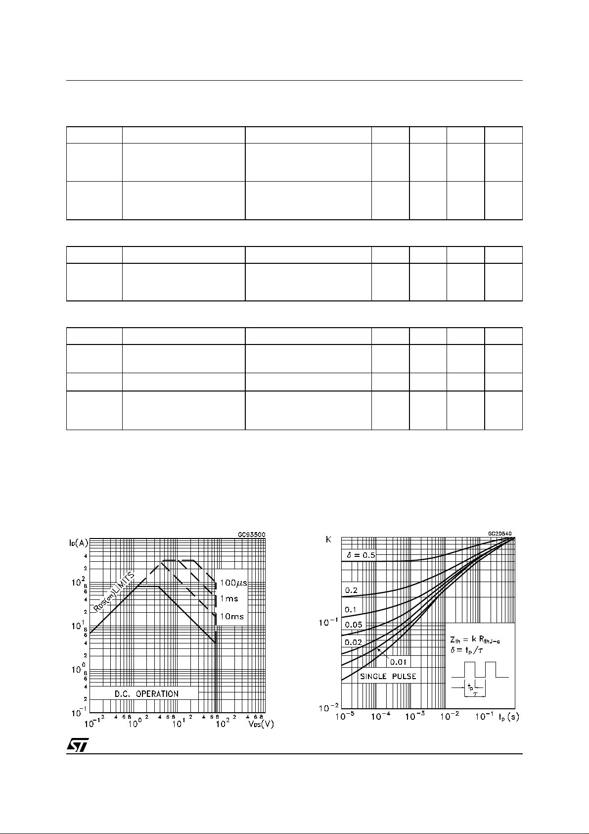
Thermal ImpedanceSaf e Operating Ar ea
3/11
Page 4
STB80NF75L/-1/ STP80NF75L
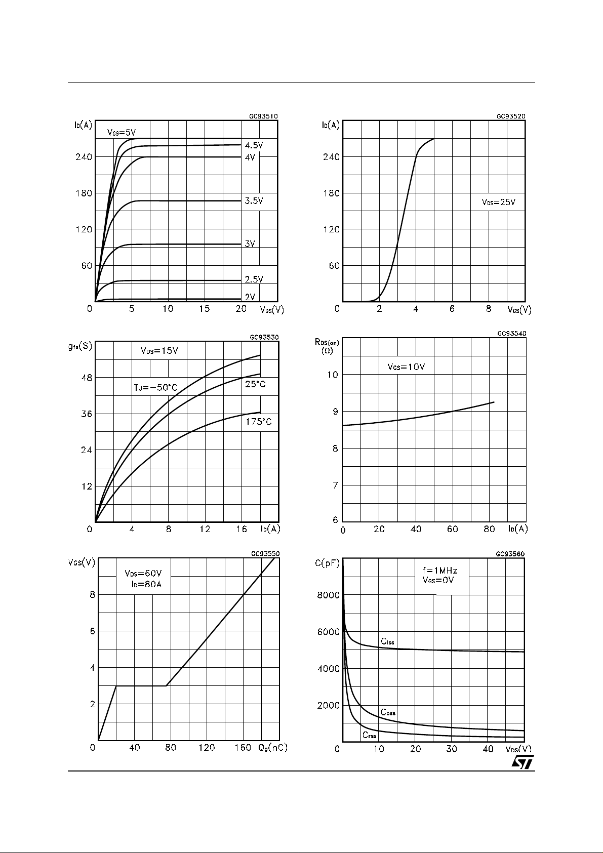
Output Characteristics Transfer Characteristics
Transconductance Static Drain-source On Resistance
Gate Charge vs Gate-source Voltage Capacitance Variations
4/11
Page 5
STB80NF75L/-1/ STP80NF75L
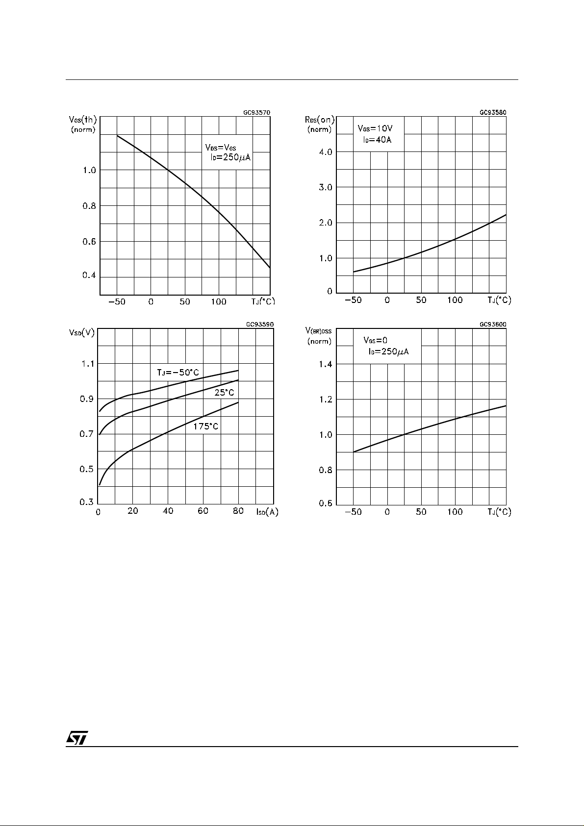
Normalized Gate Threshold Voltage vs Temperature Normalized on Resistance vs Temperature
Source-drain Diode Forward Characteristics Normalized Breakdown Voltage vs Temperature.
. .
5/11
Page 6
STB80NF75L/-1/ STP80NF75L
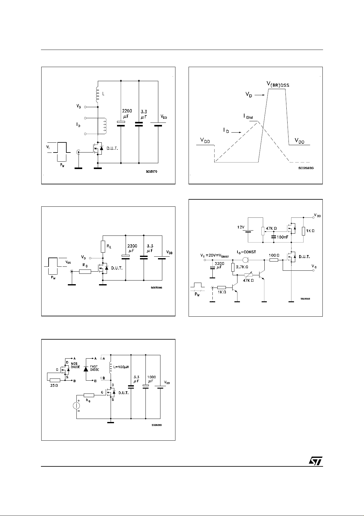
Fig. 1: Unclamped Inductive Load Test CircuitFig. 1: Unclamped Inductive Load Test Circuit Fig. 2: Unclamped Inductive Waveform
Fig. 3: Switching Times Test Circuits For Resistive
Load
Fig. 5: Test Circuit For Inductive Load Switching
And Diode Recovery Times
Fig. 4: Gate Charge test Circuit
6/11
Page 7
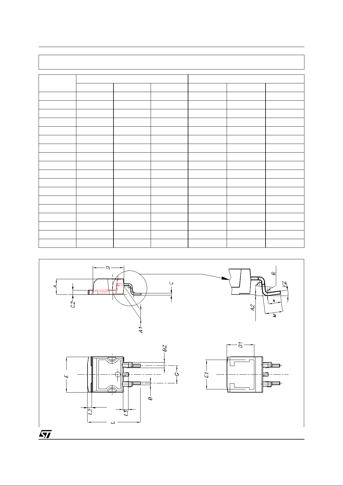
D2PAK MECHANICAL DATA
STB80NF75L/-1/ STP80NF75L
DIM.
A 4.4 4.6 0.173 0.181
A1 2.49 2.69 0.098
A2 0.03 0.23 0.001 0.009
B 0.7 0.93 0.028 0.037
B2 1.14 1.7 0.045 0.067
C 0.45 0.6 0.018 0.024
C2 1.21 1.36 0.048 0.054
D 8.95 9.35 0.352 0.368
D1 8 0.315
E 10 10.4 0.394 0.409
E1 8.5 0.334
G 4.88 5.28 0.192 0.208
L 15 15.85 0.591 0.624
L2 1.27 1.4 0.050 0.055
L3 1.4 1.75 0.055 0.069
M 2.4 3.2 0.094 0.126
R 0.4 0.016
V2 0° 8° 0° 8°
MIN. TYP. MAX. MIN. TYP. TYP.
mm. inch.
0.106
7/11
Page 8

STB80NF75L/-1/ STP80NF75L
E
TO-220 MECHANICAL DATA
DIM.
MIN. TYP. MAX. MIN. TYP. MAX.
A 4.40 4.60 0.173 0.181
C 1.23 1.32 0.048 0.051
D 2.40 2.72 0.094 0.107
D1 1.27 0.050
E 0.49 0.70 0.019 0.027
F 0.61 0.88 0.024 0.034
F1 1.14 1.70 0.044 0.067
F2 1.14 1.70 0.044 0.067
G 4.95 5.15 0.194 0.203
G1 2.4 2.7 0.094 0.106
H2 10.0 10.40 0.393 0.409
L2 16.4 0.645
L4 13.0 14.0 0.511 0.551
L5 2.65 2.95 0.104 0.116
L6 15.25 15.75 0.600 0.620
L7 6.2 6.6 0.244 0.260
L9 3.5 3.93 0.137 0.154
DIA. 3.75 3.85 0.147 0.151
mm inch
A
C
D
D1
L2
F1
L5
Dia.
G1
F
F2
L9
G
H2
L7
L6
L4
P011C
8/11
Page 9

STB80NF75L/-1/ STP80NF75L
TO-262 (I2PAK) MECHANICAL DATA
DIM.
MIN. TYP. MAX. MIN. TYP. MAX.
A 4.4 4.6 0.173 0.181
A1 2.49 2.69 0.098 0.106
B 0.7 0.93 0.027 0.036
B2 1.14 1.7 0.044 0.067
C 0.45 0.6 0.017 0.023
C2 1.23 1.36 0.048 0.053
D 8.95 9.35 0.352 0.368
e 2.4 2.7 0.094 0.106
E 10 10.4 0.393 0.409
L 13.1 13.6 0.515 0.531
L1 3.48 3.78 0.137 0.149
L2 1.27 1.4 0.050 0.055
mm inch
C
A
A1
C2
B2
B
e
E
L1
L2
D
L
P011P5/E
9/11
Page 10
STB80NF75L/-1/ STP80NF75L
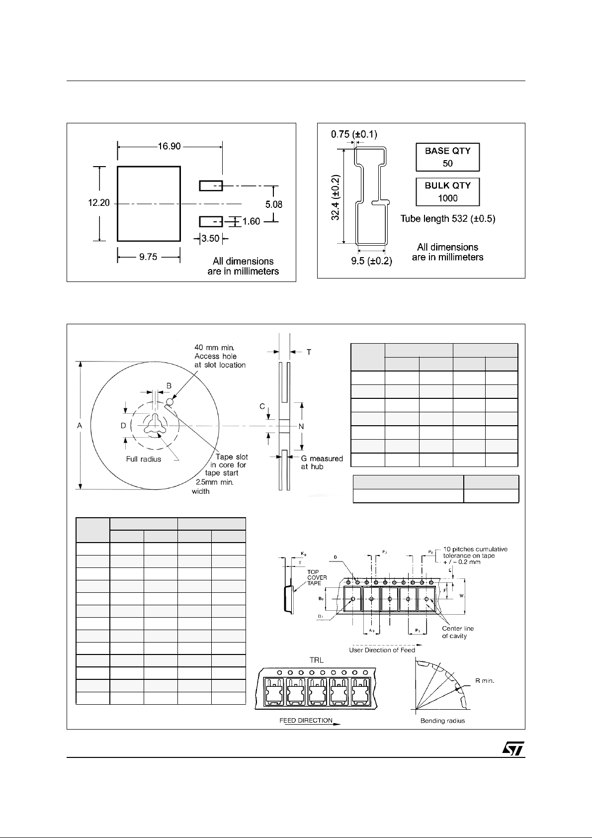
D2PAK FOOTPRINT
TAPE AND REEL SHIPMENT (suffix ”T4”)*
TUBE SHIPMENT (no suffix)*
REEL MECHANICAL DATA
DIM.
A 330 12.992
B 1.5 0.059
C 12.8 13.2 0.504 0.520
D 20.2 0.795
G 24.4 26.4 0.960 1.039
N 100 3.937
T 30.4 1.197
mm inch
MIN. MAX. MIN. MAX.
TAPE MECHANICAL DATA
DIM.
A0 10.5 10.7 0.413 0.421
B0 15.7 15.9 0.618 0.626
D 1.5 1.6 0.059 0.063
D1 1.59 1.61 0.062 0.063
E 1.65 1.85 0.065 0.073
F 11.4 11.6 0.449 0.456
K0 4.8 5.0 0.189 0.197
P0 3.9 4.1 0.153 0.161
P1 11.9 12.1 0.468 0.476
P2 1.9 2.1 0075 0.082
R50 1.574
T0.25 0.35 .0.0098 0.0137
W 23.7 24.3 0.933 0.956
mm inch
MIN. MAX. MIN. MAX.
* on sales type
10/11
BASE QTY BULK QTY
1000 1000
Page 11

STB80NF75L/-1/ STP80NF75L
Information furnished is believed to be accurate and reliable. However, STMicroelectronics assumes no responsibility for the consequences
of use of such information nor for any infringement of patents or other rights of third parties which may result from its use. No license is granted
by implic ation or otherwise under any patent or patent right s of STMicroelectronics. Specifications menti oned in this p ublication are subje ct
to change without notice. This publication supersedes and replaces all information previously supplied. STMicroelectronics products are not
authorized for use as criti cal component s in l i fe support devi ces or systems without express written appr oval of STMicroe l ectronics.
The ST logo is registered trademark of STMicroelectronics
2001 STMi croelectronics - All Rights Reserved
All other na m es are the property of their respective owners.
Australi a - Brazil - Cana da - China - Finland - France - Germ any - Hong Kong - I ndia - Israel - Ital y - Japan - Malaysia - Malta - Morocco -
Singap ore - Spain - Sweden - Switzerland - United Ki ngdom - United States.
STMicroelectronics GROUP OF COMPANIES
http:// www.st.com
11/11
 Loading...