

Page 1
Ordering number : EN6025
SPI-236-17
Ultraminiature photointerrupter
(single-transistor type)
Features
• GaAs Infrared LED plus Single Phototransistor
• Photo-Interrupter
• Contact type
• Compact type : H3.25 ✕ L5.0 ✕ W4.5mm
• Application : For the general public welfare
Absolute Maximum Ratings at Ta=25°C, 65%RH (as per JIS C 7032 )
Parameter Symbol Rating Unit
1
Forward Current
Input LED
Reverse Voltage V
Power Dissipation P
Collector-Emitter Voltage V
Output
Phototransistor
Emitter-Collector Voltage V
Collector Curren I
Power Dissipation P
Operating Temperature Topr --20 to +80 °C
Storage Temperature Tstg --30 to +85 °C
Soldering T emperature
1
*
See forward current derating
2
*
Soldering conditions : time : max. 3sec; clearance : min. 1mm from lower stay
*
2
*
I
F
R
D
CEO
ECO
C
C
T sol 260 °C
GaAs Infrared LED
SPI-236-17
50 mA
5V
70 mW
20 V
5V
20 mA
70 mW
Electro-Optical Characteristics at Ta=25°C, 65%RH
Parameter Symbol Condition Min. Typ. Max. Unit
Input
Forward Voltage V
Reverse Current I
Output Dark Current I
Collector Output Current I
Coupled
Collector Emitter
Saturation Voltage
Rise Time tr
Fall Time tf
1
*
Measurement Circuit of Collector Current
2
*
Table of Classification of Collector Output
CEO
VCE(sat) IF=10mA, IC=50µA -- -- 0.5 V
IF=10mA 1.0 1.15 1.4 V
F
VR= 5 V -- -- 1 0 µ A
R
IF=0mA, VCE=10V -- 10 200 nA
IF=10mA, VCE=5V
C
VCC=5V, RL=100Ω
IC=1mA
IF=10mA
Class A B C
Ic (µA) 880 to 460 635 to 330 460 to 240
SANYO Electric Co.,Ltd. Semiconductor Company
TOKYO OFFICE Tokyo Bldg., 1-10, 1 Chome, Ueno, T aito-ku, TOKYO, 110-8534 JAPAN
1
*
240 500 880 µA
-- 5 -- µs
-- 5 -- µs
VCE=5V
Ic
A
72199 GI, (MI
)
No.6025 1/6
Page 2
SPI-236-17
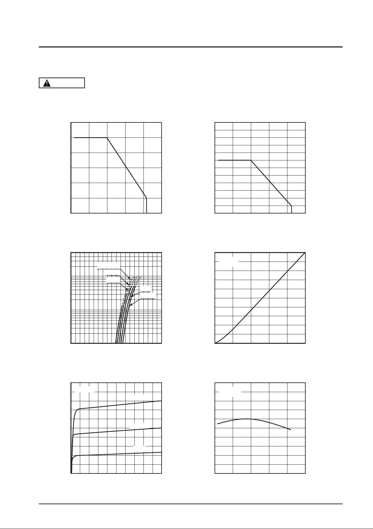
Typical Characteristics
CAUTION
These numerical value show the electrical and optical characteristics of this product, and not assure this contents.
Forward Current vs. Ambient Temperature
60
50
(mA)Collector Current I
40
F
30
20
Forward Current I
10
0
--25 0 25 50 75 100
Ambient Temperature Ta (°C)
Forward Current vs. Forward Voltage
500
Ta=75°C
50°C
25°C
0°C
--25°C
(mA)
F
100
50
10
(Rating)
Power Dissipation vs. Ambient Temperature
120
100
80
60
40
Power Dissipation P (mW)Relative Collector Current (%)
20
0
--25 0 25 50 75 100
Ambient Temperature Ta (°C)
(Rating)
Collector vs. Forward Current
1000
VCE=5V
Ta=25°C
800
(µA)
C
600
400
5
Forward Current I
1
0 0.5 1 1.5 2
Forward Voltage VF (V)
Collector Current vs. Collector-emitter Voltage
1000
Ta=25°C
800
(µA)
C
600
400
200
0
0510
Collector-emitter Voltage VCE (V)
IF=15mA
10mA
5mA
Collector Current I
200
0
048121620
Forward Current IF (mA)
Relative Collector Current vs. Ambient Temperature
140
IF=10mA
VCE=5V
120
100
80
60
40
--25 0 25 50 75 100
Ambient Temperature Ta (°C)
No.6025 2/6
Page 3

SPI-236-17
Typical Characteristics
CAUTION
These numerical value show the electrical and optical characteristics of this product, and not assure this contents.
Collector-emitter Saturation Voltage vs.
0.18
(V)
CE (sat)
0.16
0.14
0.12
0.10
Ambient Temperature
IF=10mA
IC=50µA
Collector Dark Current vs. Ambient Temperature
-6
10
VCE=10V
5
(A)
-7
10
CEO
5
-8
10
5
-9
10
5
Collector Dark Current I
0.08
Collector-emitter Saturation V oltage V
--25 0 25 50 75 100
Ambient Temperature Ta (°C)
-10
10
--25 0 25 50 75 100
Ambient Temperature Ta (°C)
Response Time vs. Load Resistance Test Circuit for Response Time
1000
IFP=10mA
500
VCC=5V
tf
Ta=25°C
100
)
S
50
Response (µ
10
5
1
0.1 0.5 1 5 10 50 100
tr
I
FP
V
CC
R
D
R
L
I
FP
tr
V
out
V
out
tf
90%
10%
Load Resistance RL (kΩ)
Relative Collector Current vs. Shield Distance (1) Relative Collector Current vs. Shield Distance (2)
120
100
IF=10mA
VCE=5V
Ta=25°C
120
100
IF=10mA
VCE=5V
Ta=25°C
80
60
40
Relative Collector Current (%)
20
0
--2 --1 0 1 2 3
Detector center
Shield Distance d (mm)
Shield
--
d
80
Shield
--
+
0
60
40
Relative Collector Current (%)
20
0
--2 --1 0 1 2 3
d
0
+
Detector center
Shield Distance d (mm)
No.6025 3/6
Page 4

SPI-236-17
0.5, Max 0.1
3
Ph.Tr LED
1.5
5 ± 0.3
2 ± 0.3
1
2
1.5
2.4
Pin No.
2.5
Pin connection
1. Common (Anode)
2. LED Cathode
3
4.5
3. Ph. Tr Emitter
Injection gate
11
2.8
2.7
0.25 3.5
0.25
C0.5
0.25
1.5
2.4
Optical C / L
3.25
2.9
3--0.4
1.3
0.3, Max 0.1
2
Tolerance : ±0.2
Unit : mm
No.6025 4/6
Page 5

SPI-236-17
Package dimensions and Pin connection
As stated in the sttached paper. (No.6025 4/6)
Soldering conditions
(1) Temperature : Max. 260°C
(2) Time : Max. 3 sec
(3) Clearance : Min. 1mm from stay (include PCB thickness)
PRECAUTIONS
(1) Bending a lead should avoid. However, when bending is necessary, take care the next items.
q Bending a lead must be done before soldering.
w Bending a lead must be done in the states of fixing leads and no stress for the regin part. Because it is possible that
stress for the regin part cause troubles such as gold wire breaking and so on.
e A lead must be bend under the stay.
r Do not bend the same position of leads more than twice.
(2) The hole pitch of a circuit board must fit to the lead pitch.
(3) Two stays coupling LED and Ph. Tr should be isolated from any PCB pattern or any lead.
(4) Take core the following when soldering.
q Do not heat a product under any stress (a twist and so on) to leads.
w Do not heat a product in the states of operating force to the regin part.
(5) Use the flux which contain no chlorine, have no corrosion and do not need washing.
(6) Be careful that flux or other chemicals do not attach to the luminous surface and passive surface.
Min. 1mm
No.6025 5/6
Page 6

SPI-236-17
CAUTION
1. No products described or contained herein are intended for use in surgical implants, life-support systems,
aerospace equipment, nuclear power control systems, vehicles, disaster / crime-prevention equipment or
the like, and the failure of which may directly or indirectly cause injury, death or property loss.
2. Anyone purchasing any products described or contained herein for an above-mentioned use shall:
1) Accept full responsibility and indemnify and defend SANYO ELECTRIC CO.,LTD., it’s affiliates,
subsidiaries and distributors or any of their officers and employees, jointly and severally, against any
and all claims and litigation and all damages, costs and expenses associated with such use.
2) Not impose any responsibility for any fault or negligence which may be cited in any such claim or
litigation on SANYO ELECTRIC CO., LTD., it’s affiliates, subsidiaries and distributors or any of
their officers and employees jointly or severally.
3. Information (including circuit diagrams and circuit parameters) disclosed herein is for example only; it is not
guaranteed for mass production, SANYO believes the information disclosed herein is accurate and reliable,
but no guarantees are made or implied regarding it’s use or any infringements of intellectual property rights
or other rights of third parties.
Precautionary instructions in handling gallium arsenic products
Special precautions must be taken in handling this product because it contains, gallium arsenic, which is
designated as a toxic substance by law. Be sure to adhere strictly to all applicable laws and regulations
enacted for this substance, particularly when it comes to disposal.
Manufactured by ; Tottori SANYO Electric Co., Ltd.
LED Division
5-318, Tachikawa-cho, Tottori City, 680-8634 Japan
TEL: +81-857-21-2137 FAX: +81-857-21-2161
No.6025 6/6
PS
 Loading...