

Page 1
SPF MIT3 02
SPF MIT3 02
Plastic Fiber Optic Transmitter including Bigfoot™ IC for MOST
Preliminary Data Sheet
Safety Hints:
Applications of new chip technologies leads to increasing optical efficiency and growing and
higher levels of optical performance. We therefore recommend that the current versions of the
IEC 825-1 and EN 60825-1 standards are taken into account right from the outset, i.e. at the
equipment development stage, and that suitable protection facilities are provided.
The data sheet of the 4-pin MOST Optical Transmitter (MIT3 02) has to be taken as preliminary.
Samples which are delivered before the qualification and the production release are engineering
samples.
Features Description
Excellent solution for converting high
speed data from TTL to Plastic Optical Fiber
(POF)
• High speed transmitter up to 50 Mbaud
• TTL Data Input (Logic to Light Function)
• 650 nm for working in a low attenuation
range of PMMA Fiber
• High coupled power in1000 micron plastic
fiber
• Low cost
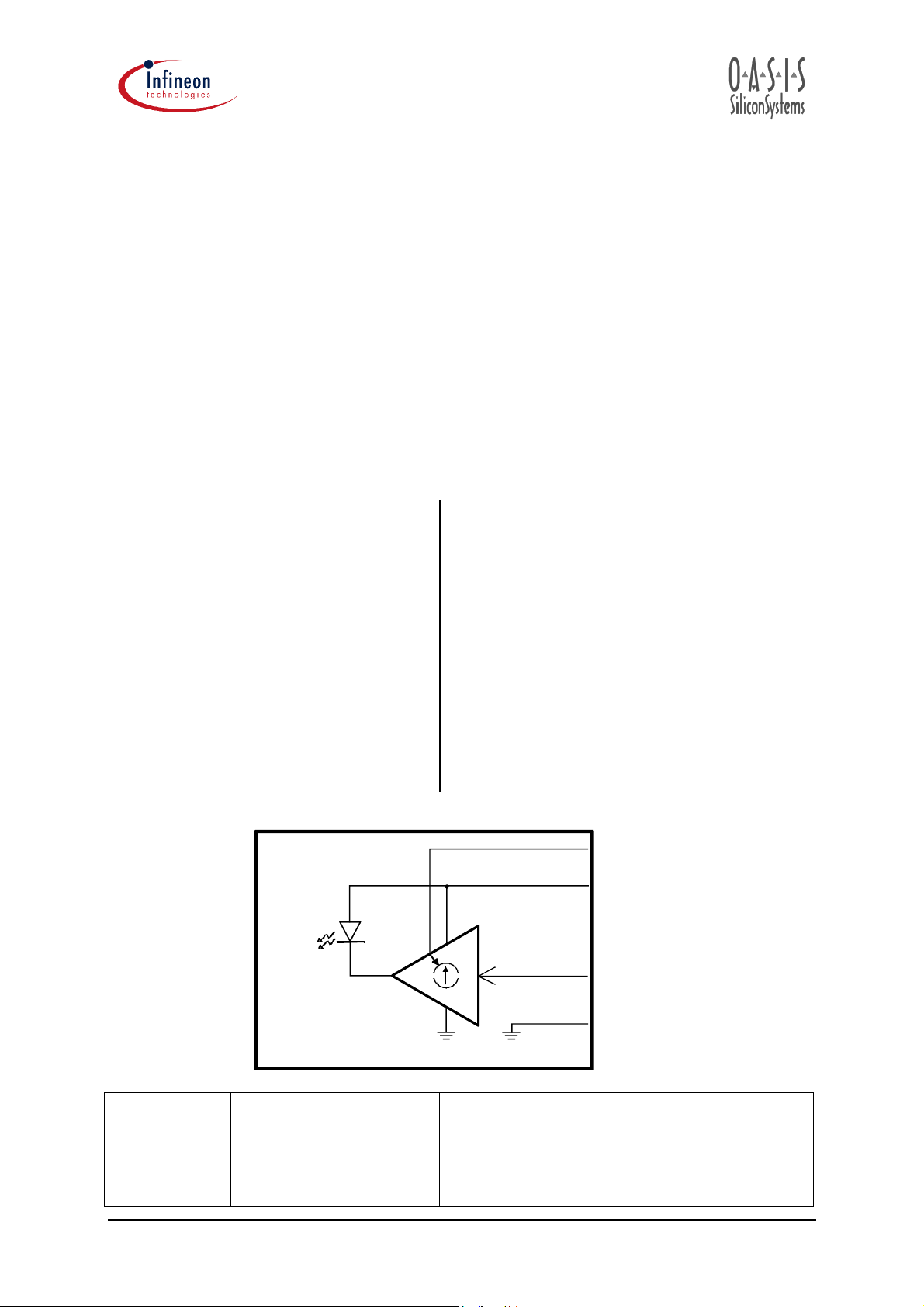
The MOST BigfootTx Plastic Fiber Optic Transmitter
is a highly integrated CMOS IC combined with a High
speed LED designed to transmit up to 25Mbit/sec
optical data which is biphase coded at up to
50Mbaud.
The internal peaking circuit minimizes PWD.
The current through the LED will be setup by an
external resistor connected to VCC. This makes it
possible to control the optical output power of the
LED.
®
Applications
• Optical Transmitter for MOST Systems
MOST BigfootTx
Actual design status:
Bigfoot IC
Revision
J CAI date code,
package type device marking Data sheet is valid
MIT3 02
4: Control
¥
3: Vcc
¥
1: TX_DATA
¥
2: GND
¥
since
15-Jan-03
MIT3 02
Preliminary Product Information Infineon AG CONFIDENTIAL
15-Jan-03 OASIS SiliconSystems AG Page 1
Page 2

Maximum Ratings
SPF MIT3 02
Parameter Symbol Min Max Unit
Storage Temperature Range T
Junction Temperature T
Soldering Temperature
(>2.5 mm from case bottom t≤5s)
Power Dissipation P
Power Supply Voltage V
CCMax
STG
T
TOT
J
S
-40 100 °C
-40 100 °C
- 235 °C
- 300 mW
-0.5 6.0 V
Recommended Operating Conditions
Parameter Symbol Min Max Unit
Supply Voltage V
Operating Temperature Range
=13.5 kOhm)
(R
ext
CC
T
A
4.75 5.25 V
-40 85
°C
All the data in this specification refers to the operating conditions above unless
otherwise stated.
Optical Signal Characteristics
(22.5 Mbit/s MOST Data, Vcc=4.75 .. 5.25 V)
Parameter Symbol Min Typ Max Unit
Peak wavelength at TA=25°C
Temperature coefficient λ
Peak
Peak wavelength at TA=-40..85°C
Spectral bandwidth (FWHM)
Average Output Power coupled into plastic fiber
=25°C, R
at T
A
Temperature coefficient P
=15 kOhm, see Note 1
ext
opt
Average Output Power coupled into plastic fiber
=-40..85°C, R
at T
A
=15 kOhm, see Note 1
ext
Average Output Power coupled into plastic fiber
=-40..85°C, R
at T
A
=15 kOhm, over lifetime,
ext
see Note 1
Gain in P
when using 13.5 KOhm instead of
opt
15 KOhm
Optical Rise Time (20% - 80%) t
Optical Fall Time (20% - 80%) t
Extinction Ratio r
Pulse Width Variation, see Note 2 t
Average Pulse Width Distortion, see Note 2 t
λ
Peak25
TCλ
λ
Peak
Delta
P
opt25, O
TC
Popt
P
opt
P
opt, lifetime
r
f
e
PWV
APWD
λ
640 650 660 nm
- 0.16 - nm/K
630 650 670 nm
-2030nm
-7.4
(185)
-5.2
(300)
-3.6
(435)
dBm
(µW)
-- 0.4-%/K
-8.6
(140)
-9.6
(110)
-5.2
(300)
-5.2
(300)
-3.1
(490)
-2.1
(615)
dBm
(µW)
dBm
(µW)
0.35 0.4 0.45 dB
-46ns
-46ns
10 11 - dB
20.9 - 24.4 ns
-0.5 - 1.5 ns
Note 1: The output power coupled into plastic fiber P
is measured with a large area detector at the
opt
end of a short length of a fiber (about 30 cm), which is ideally coupled to the Sidelooker. This value
must not be used for calculating the power budget for a fiber optic system with a long fiber because the
numerical aperture of plastic fibers decreases on the first meters.
Therefore the fiber seems to have a higher attenuation over the first few meters compared with the
specified value.
Due to the direct coupling of the fiber to the LED at the end of the short fiber UMD (uniform mode
distribution) will be observed. Therefore the following section of the cable has higher losses compared
with EMD (equilibrium mode distribution).
Note 2: The electrical input signal fulfills t
= 22.9 ns and t
PWV(min)
PWV(max)
= 24.1 ns. For further details
see page 3.
Preliminary Product Information Infineon AG CONFIDENTIAL
15-Jan-03 OASIS SiliconSystems AG Page 2
Page 3

SPF MIT3 02
Pulse Width Variation (t
) and Average Pulse Width Distortion (t
PWV
APW D
)
The SPF MIT3 02 generates negative Puls Width Distortion. This means the optical output signal is
shortened compared to the electrical input signal. Therefore the parameters t
PWV
and t
do not meet
APWD
the MOST Specification of Physical Layer Rev 1.0 (MOST SPL Rev. 1.0) either at the electrical input
signal (SP1 in the MOST SPL Rev. 1.0) or at the optical output signal (SP2 in the MOST SPL Rev.
1.0). This characteristic is shown in the following table.
Parameter Symbol Min Max Min Max Unit Remarks
Pulse Width
Variation
Average Pulse
Width Distortion
t
PWV
t
APWD
Electrical
Input Signal
22.9 24.1 20.9 24.4 nsa
1.0 1.5 -0.5 1.5 ns
Optical
Output Signal
Optical Output Signal
according to MOST
Specification of
Physical Layer Rev.
1.0
Pulse Width
Variation
Average Pulse
Width Distortion
t
PWV
t
APWD
21.1 23.1 19.1 23.4 nsb
-0.5 0.5 -2.0 0.5 ns
Electrical Input
Signal according to
MOST Specification
of Physical Layer
Rev. 1.0
Based on this table, the MOST System may be considered by two aspects:
a) In order to meet the MOST SPL Rev 1.0 at SP2 the t
PWV
and t
at SP1 have to be longer than
apwd
described in the MOST SPL Rev. 1.0. This can be achived e.g. by using OS8104 as MOST transceiver
chip.
b) If the MOST SPL Rev. 1.0 is met regarding t
PWV
and t
at SP1, then the output signal SP2 is
apwd
systematically shortened. Within a MOST System, this characteristic can be compensated by the
optical receiver which detects the signal at SP3. For this compensation, the optical receiver has to be
specified in a range which is smaller than the range described in the MOST SPL Rev. 1.0. For a
detailed evaluation of system behavior, see paper “OS8300 Revision J behavior on SP2 (optical output
signal)” from Oasis SiliconSystems.
Preliminary Product Information Infineon AG CONFIDENTIAL
15-Jan-03 OASIS SiliconSystems AG Page 3
Page 4

DC Characteristics
Parameter Symbol Min Typ Max Unit
SPF MIT3 02
Low Level Input Voltage V
High Level Input Voltage V
Input Leakage Current
=5.0V, VI=0.0V or VI=5.0V)
(V
CC
Input Capacitance C
Input Resistance R
Supply Current (R
= 15 kOhm) ON state,
ext
IL
IH
I
L
I
I
I
CC
biphase coded data, see Note 3
Supply Current (R
= 15 kOhm) OFF state,
ext
I
LP2
see Note 4
Note 3: The current through the LED and therefore the optical output power and overall power
consumption depends on the settings of R
. The nominal value for R
ext
optical output power is about –3dB of the nominal value. Typical behaviour see Fiure below.
Important: The external resistor of R
out of this range functionality may not be given over the whole temperature range and the
R
ext
device lifetime. Using values below 13K for R
must be within the range of 13.5K to 33K. For values of
ext
can damage the transmitter.
ext
-0.3 - 0.8 V
2.0 - VCC + 0.3 V
--+/- 20µA
-- 7 pF
100 - - kOhm
-25 35 mA
-- 1 mA
is 15K. With R
ext
=30K the
ext
Note 4: The transmitter jumps to low power mode after TX DATA is low for max. 18µs If the transmitter
is in low power mode it is switched ON 5µs (max.) after TX DATA starts toggling.
AC Electrical Characteristics
Parameter Test Conditions Symbol Min Typ Max Unit
Power Supply
Rejection Ratio
Power Up Time Zero à MOST Data T
Power Down Time MOST Data à Zero T
Input Rise Time t
Input Fall Time t
25 MHz Power Supply
Noise
PSRR - 30 - dB
PU
PD
TLH
THL
1.0 2.5 5.0 µs
- - 18.0 µs
--5ns
--5ns
Preliminary Product Information Infineon AG CONFIDENTIAL
15-Jan-03 OASIS SiliconSystems AG Page 4
Page 5
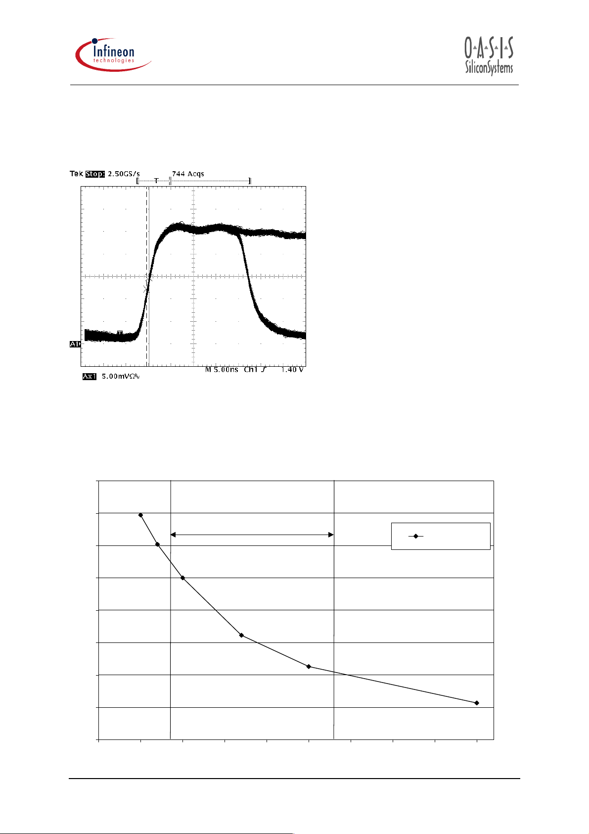
Typical Output Signal
Measured with fast optical receiver (Graviton SPD-1) with 15 kOhm external resistor and 22.579 Mbit/s
SPF MIT3 02
MOST Data at T
=25°C.
A
Typical Dependency of Average Output Power P
(22.5 MBit MOST Data/ VCC=5 V / TA=25°C)
160
Average Optical Power [%]
140
120
100
80
60
40
20
range for R
13.5 K..33 K
:
ext
on external Resistor R
opt
optical power
ext
0
5 101520253035404550
External Resistor R
Preliminary Product Information Infineon AG CONFIDENTIAL
15-Jan-03 OASIS SiliconSystems AG Page 5
ext [KOhm]
Page 6
SPF MIT3 02
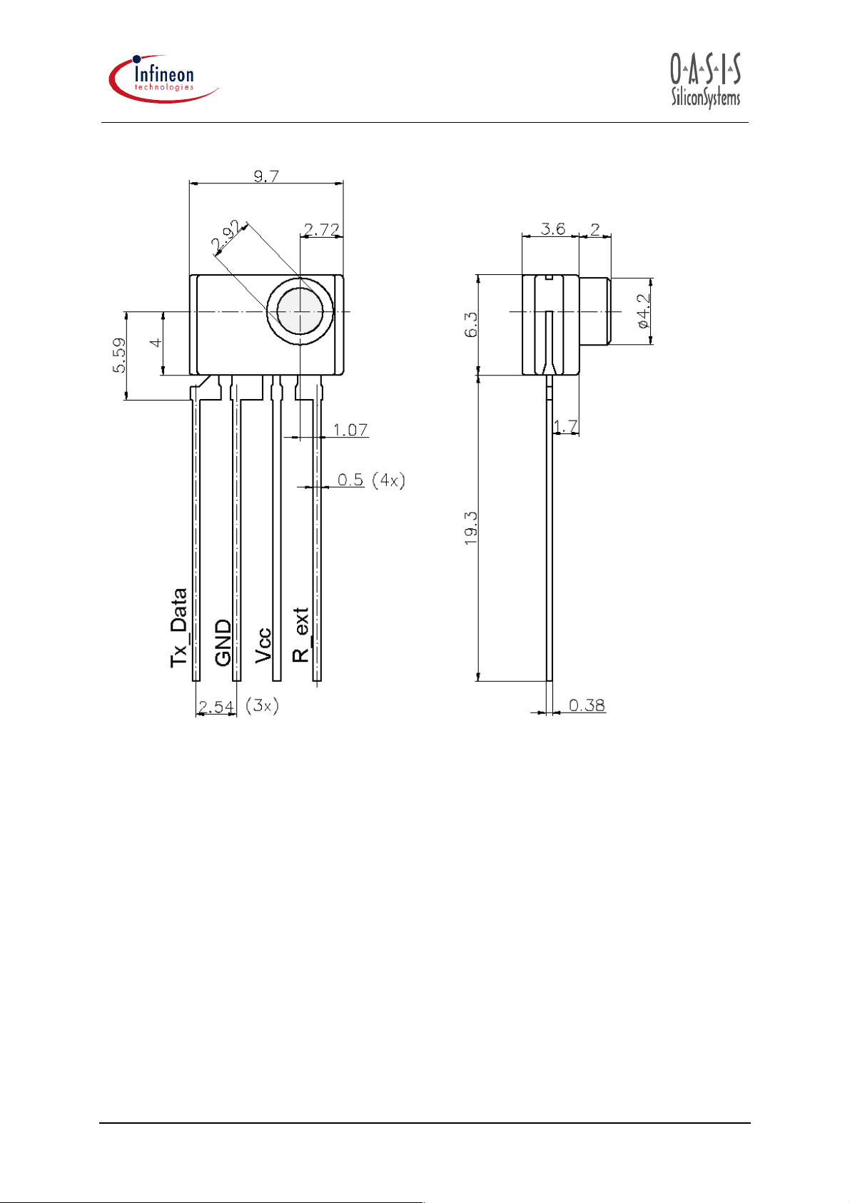
Mechanical Design MIT3 02: CAI package (cavity as interface)
Lot number, production week, component type are given on CAI backside by laser
marking (for details see marking specification).
Preliminary Product Information Infineon AG CONFIDENTIAL
15-Jan-03 OASIS SiliconSystems AG Page 6
Page 7
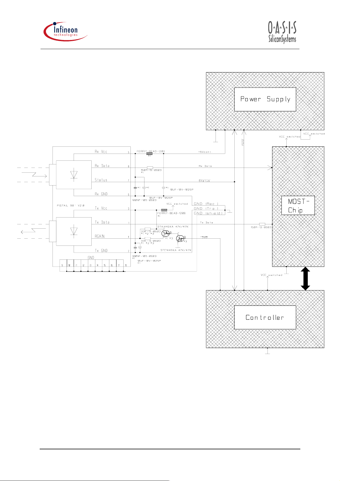
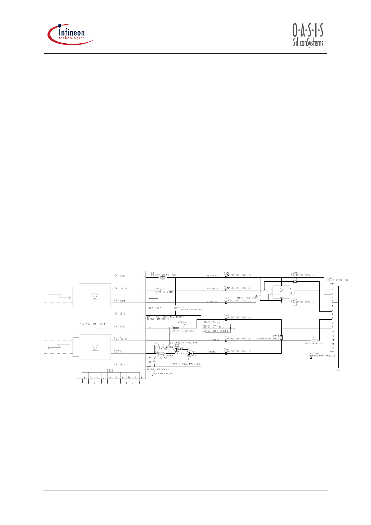
Application Circuit:
SPF MIT3 02
*1) Place these components as close
as possible to their corresponding
pins of the FOT.
*2) Values can change due to different
light output power of the LED.
*3) This is just a propo sal for the Rext
application. There can be used also
other circuits to switch Rext from
15K to 30K.
Design & Layout rules:
• The 100nF bypass capacitors of the FOTs must be located as close as possible between the pins
Vcc and GND of the FOTs. Use ceramic caps and tantalum caps with low ESR.
• Also the inductor/ferrite bead (receiver) and the -3dB - control circuit (transmitter) must be placed
as close as possible to the FOTs. We prefer ferrite beads (e.g. type 74279214 Würth Elektronik)
since the d.c. resistance is very low. If other inductors are used the d.c. resistor should be less than
3Ohm.
• For EMC a ferrite bead should be connected to the power supply close to the transmitter and the
Preliminary Product Information Infineon AG CONFIDENTIAL
15-Jan-03 OASIS SiliconSystems AG Page 7
Page 8
receiver. Do not use only one ferrite bead together for receiver and transmitter!
• For the ground connection a ground plane is recommended (Y-structure). That means the ground
planes of the transmitter, the receiver and the shielding must be separated. The three ground
planes should be connected together behind the bypass capacitors (refer to the PCB design below).
This ground signal should be connected directly to the ground plane of the MOST controller (e.g.
OS8104) and the power supply on the top layer and/or bottom layer and ground layer as it is
indicated in the example below.
• If a multi layer design is used the ground layer must have the same ground separation like shown
for the top layer!
• A serial resistor in the Rx/Tx data line will also reduce EMC - problems. For Rx the resistor must be
placed near the receiver - for Tx the resistor must be placed near the MOST controller chip. The
value depends from the distance between the FOTs and the MOST chip (< 5cm) and can be in the
range of up to 150R. Higher values for the resistors will increase jitter and can therefore cause
locking problems of the MOST PLL!
• The Rx/Tx signals should not be routed parallel over a long distance but may be embedded with
ground copper, if possible.
• The GND pin and the pin of Rext (15K - resistor) of the transmitter are used for heat dissipation.
Therefore there should be a good connection to the PCB à no isolation gaps! Both pins should dip
into a copper area (see layout example below).
Layout example:
SPF MIT3 02
The reference board from OASIS Silicon Systems follows the requirements above. The schematic is
very similar to the example above, but does not include the connection to the power supply, the
OS8104 or the microcontroller.
The examples below for top- and bottom layer is the layout of the reference design board and shows
how the layout around the optical receiver and transmitter should look like.
It is strongly recommended to follow this examples in your design to get best performance!
Note:
The buffer circuit (IC1), the connectors and jumpers in the middle to the right section of the schematic
are only for use of the reference board and will not be necessary for your HW - design.
Preliminary Product Information Infineon AG CONFIDENTIAL
15-Jan-03 OASIS SiliconSystems AG Page 8
Page 9
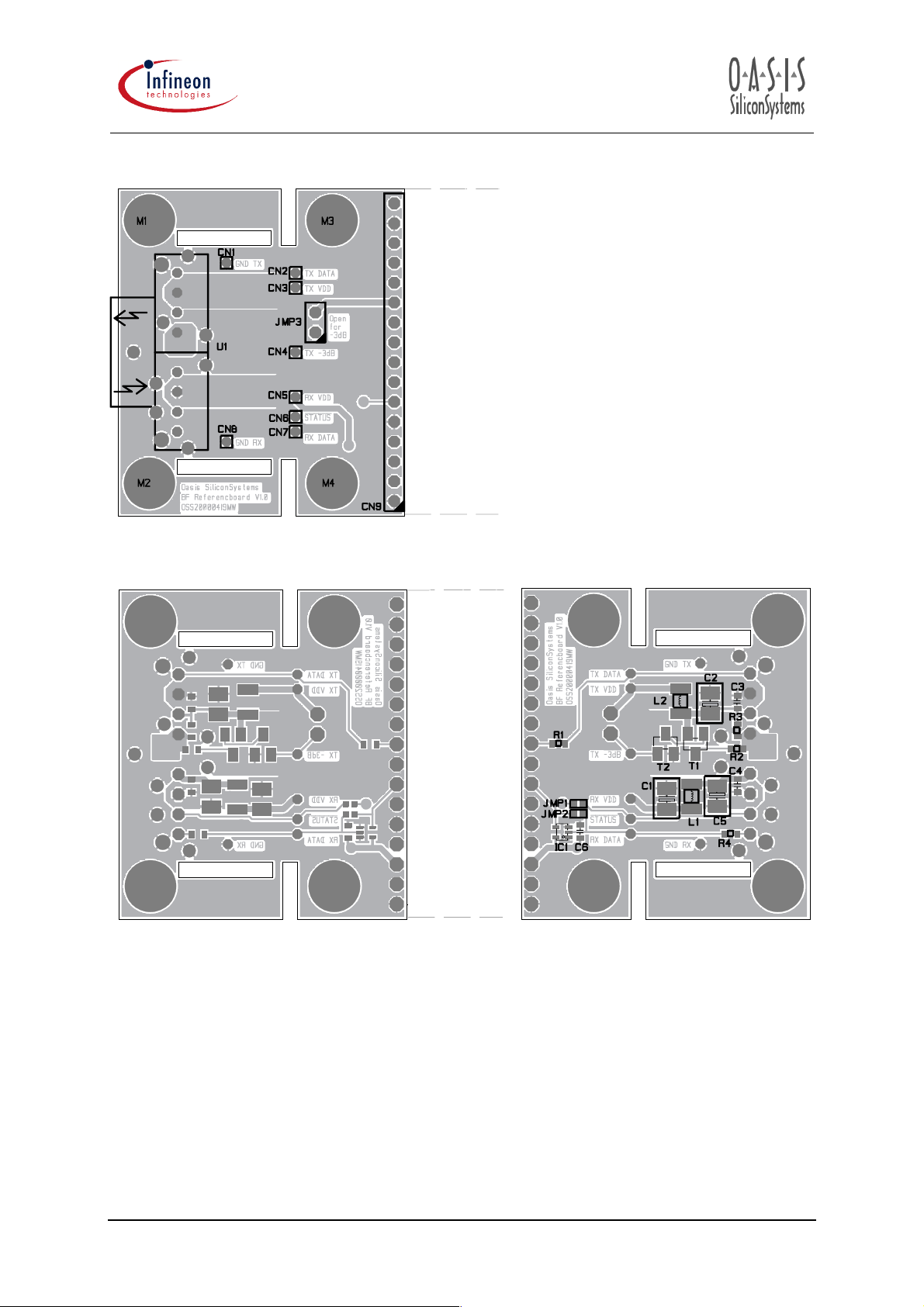
Top Layer with 180° version of the pigtail:
GND - BUS to OS8104 and Power Supply
SPF MIT3 02
Bottom Layer (seen from the top side of the PCB): Bottom Layer: Bottom side / positions
GND - BUS to OS8104 and Power Supply
Preliminary Product Information Infineon AG CONFIDENTIAL
15-Jan-03 OASIS SiliconSystems AG Page 9
Page 10

Other items:
• The shown circuit for the –3dB attenuation is just a proposal. Also any other circuit which can
SPF MIT3 02
double the value of R
is permitted.
ext
• Due to the fact that the optical average level jumps if the power control signal (/-3dB) is
toggled there can occur LOCK/coding – errors at the following device for a short time. This is
not very critical, since it does occur only in diagnosis mode. After a time of 10ms the device should
lock again if the optical attenuation between the devices is not too high.
• The Rx and Tx signals can be measured by using standard probes (>1M/<10pF). However, if the
signal quality is very bad and the LOCK signal of the MOST chip is flaky connecting a passive probe
to the Rx signal can cause the MOST chip to lock better or worse to the signal. This is due to the
capacitance of the analog probe which is usually in the range of 8..12pF and shifts the phase and
PWD of the signal. In this case an active probe with a capacitance of less than 1pF is
recommended.
• The reference test board which corresponds to the layout examples above is available at the
Oasis Silicon System AG.
Preliminary Product Information Infineon AG CONFIDENTIAL
15-Jan-03 OASIS SiliconSystems AG Page 10
Page 11

History of Design and Specification Status of MOST Transmitter:
SPF MIT3 02
Data Sheet
Status
Bigfoot IC
Revision
device
marking
02-Dec-02 J Date code
MIT3 02
15-Jan-03 J date
code,
MIT3 02
comments, cause of change,
important differences to last Status
New release
p. 2: Update of Note 2
p. 3: Section Pulse Width Variation (t
Width Distortion (t
APWD
) added
) and Average Pulse
PWV
Preliminary Product Information Infineon AG CONFIDENTIAL
15-Jan-03 OASIS SiliconSystems AG Page 11
Page 12

Notes:
SPF MIT3 02
Preliminary Product Information Infineon AG CONFIDENTIAL
15-Jan-03 OASIS SiliconSystems AG Page 12
 Loading...