

Page 1
for industrial and consumer applications
LFBGA289 (15 x 15 x 1.7 mm)
Features
■ ARM926EJ-S CPU core, up to 333 MHz
■ Multilayer bus matrix, up to 166 MHz
■ Internal memories: 32 KB ROM, 8 KB SRAM
■ Memory interfaces:
– DDR controller (DDR2-666, LPDDR-333),
8-/16-bit
– Serial NOR Flash controller
– Parallel NAND Flash controller, 8-/16-bit
data bus
– Parallel NOR Flash/FPGA interface,
8-/16-bit data bus
■ Connectivity:
– 2 x USB 2.0 Host ports (integrated PHY)
– 1 x USB 2.0 Device port (integrated PHY)
– 2 x Fast Ethernet ports (external MII/RMII
PHY)
– 1 x MMC-SD card/SDIO controller
– 2 x CAN 2.0 ports
–7 x UART ports
– 3 x I2C ports: master/slave
– 3 x synchronous serial ports,
SPI/Microwire/TI protocols, master/slave
– 1 x RS485 interface
– 1 x fast IrDA interface
– 1 x legacy parallel port (IEEE 1284), slave
mode
– 10-bit ADC, 8 channels, 1 Msps
– Up to 102 GPIOs with interrupt capability
■ HMI support:
– LCD display controller, up to XGA
(1024 x 768, 24 bpp)
– Resistive touchscreen interface
– JPEG codec accelerator
– 1 x I2S digital audio port
■ Security
– Cryptographic co-processor
SPEAr320S
Embedded MPU with ARM926 core
Datasheet − production data
■ Miscellaneous functions:
– System controller, vectored interrupt
controller, watchdog, real-time clock
– Dynamic power-saving features
– 8-channel DMA controller
– 6 x 16-bit general purpose timers with
prescaler and 4 capture inputs
– 4 x PWM generators
– Debug and trace interfaces: JTAG/ETM
Applications
The SPEAr320S embedded MPU is configurable
for a range of industrial and consumer
applications such as:
■ Human machine interface (HMI) terminals
■ Factory automation / PLCs
■ Medical equipment
■ Smart energy meters and gateways
■ VoIP phones
■ Small printers
The device is hardware-compliant to the support
of both real-time (RTOS) and high-level (HLOS)
operating systems, such as Linux and Windows
Embedded Compact 7.
Table 1. Device summary
Order code
SPEAR320S-2 -40 to 85
Temp
range, ° C
Package Packing
LFBGA289
(15x15 mm,
pitch 0.8 mm)
Tr ay
April 2012 Doc ID 022508 Rev 1 1/97
This is information on a product in full production.
www.st.com
1
Page 2

Contents SPEAr320S
Contents
1 Description . . . . . . . . . . . . . . . . . . . . . . . . . . . . . . . . . . . . . . . . . . . . . . . . . 9
2 Device functions . . . . . . . . . . . . . . . . . . . . . . . . . . . . . . . . . . . . . . . . . . . 11
2.1 CPU subsystem . . . . . . . . . . . . . . . . . . . . . . . . . . . . . . . . . . . . . . . . . . . . 11
2.2 Internal memories (BootROM/SRAM) . . . . . . . . . . . . . . . . . . . . . . . . . . . 11
2.3 Multiport DDR controller (MPMC) . . . . . . . . . . . . . . . . . . . . . . . . . . . . . . 12
2.4 Serial NOR Flash controller (SMI) . . . . . . . . . . . . . . . . . . . . . . . . . . . . . . 12
2.5 Parallel NAND Flash controller (FSMC) . . . . . . . . . . . . . . . . . . . . . . . . . . 13
2.6 External memory interface (EMI) . . . . . . . . . . . . . . . . . . . . . . . . . . . . . . . 14
2.7 USB 2.0 Host ports (UHC) . . . . . . . . . . . . . . . . . . . . . . . . . . . . . . . . . . . . 14
2.8 USB 2.0 Device port (UDC) . . . . . . . . . . . . . . . . . . . . . . . . . . . . . . . . . . . 15
2.9 Fast Ethernet ports (MII/RMII) . . . . . . . . . . . . . . . . . . . . . . . . . . . . . . . . . 15
2.9.1 MII0 Ethernet controller . . . . . . . . . . . . . . . . . . . . . . . . . . . . . . . . . . . . . 15
2.9.2 RMII0 and MII1/RMII1 Ethernet controllers . . . . . . . . . . . . . . . . . . . . . . 16
2.10 MMC-SD card/SDIO controller . . . . . . . . . . . . . . . . . . . . . . . . . . . . . . . . . 16
2.11 CAN 2.0 ports . . . . . . . . . . . . . . . . . . . . . . . . . . . . . . . . . . . . . . . . . . . . . . 17
2.12 Asynchronous serial ports (UART) . . . . . . . . . . . . . . . . . . . . . . . . . . . . . . 18
2.13 I2C bus ports (I2C) . . . . . . . . . . . . . . . . . . . . . . . . . . . . . . . . . . . . . . . . . . 19
2.14 Synchronous serial ports (SSP) . . . . . . . . . . . . . . . . . . . . . . . . . . . . . . . . 19
2.15 RS485 port (RS485) . . . . . . . . . . . . . . . . . . . . . . . . . . . . . . . . . . . . . . . . . 20
2.16 Fast infrared port (IrDA) . . . . . . . . . . . . . . . . . . . . . . . . . . . . . . . . . . . . . . 20
2.17 Legacy IEEE 1284 parallel port (SPP) . . . . . . . . . . . . . . . . . . . . . . . . . . . 20
2.18 A/D converter (ADC) . . . . . . . . . . . . . . . . . . . . . . . . . . . . . . . . . . . . . . . . 21
2.19 General purpose I/Os (GPIO/XGPIO) . . . . . . . . . . . . . . . . . . . . . . . . . . . 21
2.20 LCD display controller (CLCD) . . . . . . . . . . . . . . . . . . . . . . . . . . . . . . . . . 22
2.21 Touchscreen interface (OUT_X) . . . . . . . . . . . . . . . . . . . . . . . . . . . . . . . . 22
2.22 JPEG codec accelerator (JPGC) . . . . . . . . . . . . . . . . . . . . . . . . . . . . . . . 23
2.23 Digital audio port (I2S) . . . . . . . . . . . . . . . . . . . . . . . . . . . . . . . . . . . . . . . 23
2.24 Cryptographic co-processor (C3) . . . . . . . . . . . . . . . . . . . . . . . . . . . . . . . 23
2.25 System controller (SYSCTR) . . . . . . . . . . . . . . . . . . . . . . . . . . . . . . . . . . 24
2.25.1 Reset and clock generator . . . . . . . . . . . . . . . . . . . . . . . . . . . . . . . . . . . 25
2/97 Doc ID 022508 Rev 1
Page 3

SPEAr320S Contents
2.26 Vectored interrupt controller (VIC) . . . . . . . . . . . . . . . . . . . . . . . . . . . . . . 25
2.27 Watchdog timer (WDT) . . . . . . . . . . . . . . . . . . . . . . . . . . . . . . . . . . . . . . . 26
2.28 Real-time clock (RTC) . . . . . . . . . . . . . . . . . . . . . . . . . . . . . . . . . . . . . . . 26
2.29 DMA controller (DMAC) . . . . . . . . . . . . . . . . . . . . . . . . . . . . . . . . . . . . . . 26
2.30 General purpose timers (GPT) . . . . . . . . . . . . . . . . . . . . . . . . . . . . . . . . . 27
2.31 Pulse width modulators (PWM) . . . . . . . . . . . . . . . . . . . . . . . . . . . . . . . . 27
3 Pin description . . . . . . . . . . . . . . . . . . . . . . . . . . . . . . . . . . . . . . . . . . . . 28
3.1 Pin/ball map . . . . . . . . . . . . . . . . . . . . . . . . . . . . . . . . . . . . . . . . . . . . . . . 29
3.2 Required external components . . . . . . . . . . . . . . . . . . . . . . . . . . . . . . . . 30
3.3 Dedicated pins description . . . . . . . . . . . . . . . . . . . . . . . . . . . . . . . . . . . . 30
3.3.1 Clock, reset and 3V3 comparator pins . . . . . . . . . . . . . . . . . . . . . . . . . . 30
3.3.2 Power supply pins . . . . . . . . . . . . . . . . . . . . . . . . . . . . . . . . . . . . . . . . . 31
3.3.3 Debug pins . . . . . . . . . . . . . . . . . . . . . . . . . . . . . . . . . . . . . . . . . . . . . . . 32
3.3.4 Non-multiplexed pins . . . . . . . . . . . . . . . . . . . . . . . . . . . . . . . . . . . . . . . 32
3.4 Shared IO pins (PL_GPIOs) . . . . . . . . . . . . . . . . . . . . . . . . . . . . . . . . . . . 36
3.4.1 PL_GPIO pins description . . . . . . . . . . . . . . . . . . . . . . . . . . . . . . . . . . . 36
3.4.2 Configuration modes . . . . . . . . . . . . . . . . . . . . . . . . . . . . . . . . . . . . . . . 36
3.4.3 Alternate functions . . . . . . . . . . . . . . . . . . . . . . . . . . . . . . . . . . . . . . . . . 38
3.4.4 Boot pins . . . . . . . . . . . . . . . . . . . . . . . . . . . . . . . . . . . . . . . . . . . . . . . . 39
3.4.5 GPIOs . . . . . . . . . . . . . . . . . . . . . . . . . . . . . . . . . . . . . . . . . . . . . . . . . . 39
3.4.6 Multiplexing scheme . . . . . . . . . . . . . . . . . . . . . . . . . . . . . . . . . . . . . . . 39
3.4.7 Multiplexed signals description . . . . . . . . . . . . . . . . . . . . . . . . . . . . . . . 45
3.5 PL_GPIO pin sharing for debug modes . . . . . . . . . . . . . . . . . . . . . . . . . . 62
4 Electrical characteristics . . . . . . . . . . . . . . . . . . . . . . . . . . . . . . . . . . . . 64
4.1 Absolute maximum ratings . . . . . . . . . . . . . . . . . . . . . . . . . . . . . . . . . . . . 64
4.2 Maximum power consumption . . . . . . . . . . . . . . . . . . . . . . . . . . . . . . . . . 64
4.3 Recommended operating conditions . . . . . . . . . . . . . . . . . . . . . . . . . . . . 65
4.4 Overshoot and undershoot . . . . . . . . . . . . . . . . . . . . . . . . . . . . . . . . . . . . 65
4.5 3.3V I/O characteristics . . . . . . . . . . . . . . . . . . . . . . . . . . . . . . . . . . . . . . 65
4.6 Clocking parameters . . . . . . . . . . . . . . . . . . . . . . . . . . . . . . . . . . . . . . . . 67
4.6.1 Master clock (MCLK) . . . . . . . . . . . . . . . . . . . . . . . . . . . . . . . . . . . . . . . 67
4.6.2 Real-time clock (RTC) . . . . . . . . . . . . . . . . . . . . . . . . . . . . . . . . . . . . . . 68
4.7 LPDDR and DDR2 pin characteristics . . . . . . . . . . . . . . . . . . . . . . . . . . . 69
Doc ID 022508 Rev 1 3/97
Page 4

Contents SPEAr320S
4.8 ADC pin characteristics . . . . . . . . . . . . . . . . . . . . . . . . . . . . . . . . . . . . . . 70
4.9 Power-up sequence . . . . . . . . . . . . . . . . . . . . . . . . . . . . . . . . . . . . . . . . . 71
4.10 Power-down sequence . . . . . . . . . . . . . . . . . . . . . . . . . . . . . . . . . . . . . . . 71
4.11 Reset release . . . . . . . . . . . . . . . . . . . . . . . . . . . . . . . . . . . . . . . . . . . . . . 71
5 Timing requirements . . . . . . . . . . . . . . . . . . . . . . . . . . . . . . . . . . . . . . . . 72
5.1 External interrupt timing characteristics . . . . . . . . . . . . . . . . . . . . . . . . . . 72
5.2 Reset timing characteristics . . . . . . . . . . . . . . . . . . . . . . . . . . . . . . . . . . . 72
5.3 CLCD timing characteristics . . . . . . . . . . . . . . . . . . . . . . . . . . . . . . . . . . . 72
5.4 DDR2 timing characteristics . . . . . . . . . . . . . . . . . . . . . . . . . . . . . . . . . . . 73
5.4.1 DDR2 read cycle timing characteristics . . . . . . . . . . . . . . . . . . . . . . . . . 73
5.4.2 DDR2 write cycle timing characteristics . . . . . . . . . . . . . . . . . . . . . . . . . 74
5.4.3 DDR2 command timing characteristics . . . . . . . . . . . . . . . . . . . . . . . . . 74
5.5 EMI timing characteristics . . . . . . . . . . . . . . . . . . . . . . . . . . . . . . . . . . . . 75
5.6 Ethernet MII timing characteristics . . . . . . . . . . . . . . . . . . . . . . . . . . . . . . 77
5.6.1 MII transmit timing characteristics . . . . . . . . . . . . . . . . . . . . . . . . . . . . . 77
5.6.2 MII receive timing characteristics . . . . . . . . . . . . . . . . . . . . . . . . . . . . . . 78
5.6.3 MDIO timing characteristics . . . . . . . . . . . . . . . . . . . . . . . . . . . . . . . . . . 78
5.7 Ethernet RMII timing characteristics . . . . . . . . . . . . . . . . . . . . . . . . . . . . 79
5.7.1 RMII transmit timing characteristics . . . . . . . . . . . . . . . . . . . . . . . . . . . . 79
5.7.2 RMII receive timing characteristics . . . . . . . . . . . . . . . . . . . . . . . . . . . . 79
5.8 FSMC timing characteristics . . . . . . . . . . . . . . . . . . . . . . . . . . . . . . . . . . . 80
5.9 I
2
C timing characteristics . . . . . . . . . . . . . . . . . . . . . . . . . . . . . . . . . . . . . 83
5.10 I2S timing characteristics . . . . . . . . . . . . . . . . . . . . . . . . . . . . . . . . . . . . . 84
5.11 SD timing characteristics . . . . . . . . . . . . . . . . . . . . . . . . . . . . . . . . . . . . . 85
5.12 SMI timing characteristics . . . . . . . . . . . . . . . . . . . . . . . . . . . . . . . . . . . . 86
5.13 SSP timing characteristics . . . . . . . . . . . . . . . . . . . . . . . . . . . . . . . . . . . . 87
5.13.1 SPI master mode timing characteristics (clock phase = 0) . . . . . . . . . . 88
5.13.2 SPI master mode timing characteristics (clock phase = 1) . . . . . . . . . . 89
5.14 UART timing characteristics . . . . . . . . . . . . . . . . . . . . . . . . . . . . . . . . . . . 90
6 Package information . . . . . . . . . . . . . . . . . . . . . . . . . . . . . . . . . . . . . . . . 91
Appendix A Acronyms . . . . . . . . . . . . . . . . . . . . . . . . . . . . . . . . . . . . . . . . . . . . . . 93
4/97 Doc ID 022508 Rev 1
Page 5

SPEAr320S Contents
Revision history . . . . . . . . . . . . . . . . . . . . . . . . . . . . . . . . . . . . . . . . . . . . . . . . . . . . 96
Doc ID 022508 Rev 1 5/97
Page 6

List of tables SPEAr320S
List of tables
Table 1. Device summary . . . . . . . . . . . . . . . . . . . . . . . . . . . . . . . . . . . . . . . . . . . . . . . . . . . . . . . . . . 1
Table 2. NAND Flash devices supported by the BootROM firmware . . . . . . . . . . . . . . . . . . . . . . . . 13
Table 3. SPEAr320S UART capabilities . . . . . . . . . . . . . . . . . . . . . . . . . . . . . . . . . . . . . . . . . . . . . . 18
Table 4. Pixel widths and formats available for different display types. . . . . . . . . . . . . . . . . . . . . . . 22
Table 5. Headers/abbreviations . . . . . . . . . . . . . . . . . . . . . . . . . . . . . . . . . . . . . . . . . . . . . . . . . . . . 28
Table 6. MCLK, RTC, Reset and 3.3 V comparator pins description . . . . . . . . . . . . . . . . . . . . . . . . 30
Table 7. Power supply pins description . . . . . . . . . . . . . . . . . . . . . . . . . . . . . . . . . . . . . . . . . . . . . . 31
Table 8. Debug pins description . . . . . . . . . . . . . . . . . . . . . . . . . . . . . . . . . . . . . . . . . . . . . . . . . . . . 32
Table 9. SMI pins description . . . . . . . . . . . . . . . . . . . . . . . . . . . . . . . . . . . . . . . . . . . . . . . . . . . . . . 32
Table 10. USB pins description . . . . . . . . . . . . . . . . . . . . . . . . . . . . . . . . . . . . . . . . . . . . . . . . . . . . . 33
Table 11. ADC pins description . . . . . . . . . . . . . . . . . . . . . . . . . . . . . . . . . . . . . . . . . . . . . . . . . . . . . 33
Table 12. DDR pins description . . . . . . . . . . . . . . . . . . . . . . . . . . . . . . . . . . . . . . . . . . . . . . . . . . . . . 34
Table 13. PL_GPIO pins description . . . . . . . . . . . . . . . . . . . . . . . . . . . . . . . . . . . . . . . . . . . . . . . . . 36
Table 14. Boot pins description . . . . . . . . . . . . . . . . . . . . . . . . . . . . . . . . . . . . . . . . . . . . . . . . . . . . . 39
Table 15. PL_GPIO multiplexing scheme. . . . . . . . . . . . . . . . . . . . . . . . . . . . . . . . . . . . . . . . . . . . . . 40
Table 16. Table shading . . . . . . . . . . . . . . . . . . . . . . . . . . . . . . . . . . . . . . . . . . . . . . . . . . . . . . . . . . . 44
Table 17. FSMC signals description . . . . . . . . . . . . . . . . . . . . . . . . . . . . . . . . . . . . . . . . . . . . . . . . . . 45
Table 18. EMI signals description. . . . . . . . . . . . . . . . . . . . . . . . . . . . . . . . . . . . . . . . . . . . . . . . . . . . 46
Table 19. CLCD signals description . . . . . . . . . . . . . . . . . . . . . . . . . . . . . . . . . . . . . . . . . . . . . . . . . . 48
Table 20. Touchscreen signal description . . . . . . . . . . . . . . . . . . . . . . . . . . . . . . . . . . . . . . . . . . . . . 49
Table 21. UART signals description . . . . . . . . . . . . . . . . . . . . . . . . . . . . . . . . . . . . . . . . . . . . . . . . . . 49
Table 22. CAN signals description . . . . . . . . . . . . . . . . . . . . . . . . . . . . . . . . . . . . . . . . . . . . . . . . . . . 51
Table 23. MMC-SD/SDIO controller signals description . . . . . . . . . . . . . . . . . . . . . . . . . . . . . . . . . . . 52
Table 24. PWM signals description . . . . . . . . . . . . . . . . . . . . . . . . . . . . . . . . . . . . . . . . . . . . . . . . . . 52
Table 25. GPT signals description . . . . . . . . . . . . . . . . . . . . . . . . . . . . . . . . . . . . . . . . . . . . . . . . . . . 53
Table 26. IrDA signals description . . . . . . . . . . . . . . . . . . . . . . . . . . . . . . . . . . . . . . . . . . . . . . . . . . . 53
Table 27. SSP signals description . . . . . . . . . . . . . . . . . . . . . . . . . . . . . . . . . . . . . . . . . . . . . . . . . . . 54
Table 28. I2C signals description . . . . . . . . . . . . . . . . . . . . . . . . . . . . . . . . . . . . . . . . . . . . . . . . . . . . 56
Table 29. I2S signals description . . . . . . . . . . . . . . . . . . . . . . . . . . . . . . . . . . . . . . . . . . . . . . . . . . . . 56
Table 30. SPP signals description . . . . . . . . . . . . . . . . . . . . . . . . . . . . . . . . . . . . . . . . . . . . . . . . . . . 57
Table 31. Ethernet signals description . . . . . . . . . . . . . . . . . . . . . . . . . . . . . . . . . . . . . . . . . . . . . . . . 58
Table 32. Ball sharing during debug . . . . . . . . . . . . . . . . . . . . . . . . . . . . . . . . . . . . . . . . . . . . . . . . . . 62
Table 33. Absolute maximum ratings . . . . . . . . . . . . . . . . . . . . . . . . . . . . . . . . . . . . . . . . . . . . . . . . . 64
Table 34. Maximum power consumption . . . . . . . . . . . . . . . . . . . . . . . . . . . . . . . . . . . . . . . . . . . . . . 64
Table 35. Recommended operating conditions . . . . . . . . . . . . . . . . . . . . . . . . . . . . . . . . . . . . . . . . . 65
Table 36. Overshoot and undershoot specifications. . . . . . . . . . . . . . . . . . . . . . . . . . . . . . . . . . . . . . 65
Table 37. Low voltage TTL DC input specification (3 V< V
Table 38. Low voltage TTL DC output specification (3 V< V
Table 39. Pull-up and pull-down characteristics . . . . . . . . . . . . . . . . . . . . . . . . . . . . . . . . . . . . . . . . . 66
Table 40. DC characteristics. . . . . . . . . . . . . . . . . . . . . . . . . . . . . . . . . . . . . . . . . . . . . . . . . . . . . . . . 69
Table 41. Driver characteristics . . . . . . . . . . . . . . . . . . . . . . . . . . . . . . . . . . . . . . . . . . . . . . . . . . . . . 69
Table 42. On-die termination . . . . . . . . . . . . . . . . . . . . . . . . . . . . . . . . . . . . . . . . . . . . . . . . . . . . . . . 69
Table 43. Reference voltage. . . . . . . . . . . . . . . . . . . . . . . . . . . . . . . . . . . . . . . . . . . . . . . . . . . . . . . . 69
Table 44. ADC pin characteristics . . . . . . . . . . . . . . . . . . . . . . . . . . . . . . . . . . . . . . . . . . . . . . . . . . . 70
Table 45. PL_GPIO external interrupt input timing . . . . . . . . . . . . . . . . . . . . . . . . . . . . . . . . . . . . . . . 72
Table 46. Cold reset (at power-on) . . . . . . . . . . . . . . . . . . . . . . . . . . . . . . . . . . . . . . . . . . . . . . . . . . . 72
Table 47. CLCD timing requirements . . . . . . . . . . . . . . . . . . . . . . . . . . . . . . . . . . . . . . . . . . . . . . . . . 73
Table 48. DDR2 read cycle timing requirements . . . . . . . . . . . . . . . . . . . . . . . . . . . . . . . . . . . . . . . . 73
<3.6 V) . . . . . . . . . . . . . . . . . . . . . . . . 66
DD
<3.6 V) . . . . . . . . . . . . . . . . . . . . . . . 66
DD
6/97 Doc ID 022508 Rev 1
Page 7

SPEAr320S List of tables
Table 49. DDR2 write cycle timing requirements . . . . . . . . . . . . . . . . . . . . . . . . . . . . . . . . . . . . . . . . 74
Table 50. DDR2 command timing requirements. . . . . . . . . . . . . . . . . . . . . . . . . . . . . . . . . . . . . . . . . 74
Table 51. EMI timing requirements for read cycle with acknowledgement on WAIT . . . . . . . . . . . . . 75
Table 52. EMI timing requirements for write cycle with acknowledgement on WAIT . . . . . . . . . . . . . 76
Table 53. EMI timing requirements. . . . . . . . . . . . . . . . . . . . . . . . . . . . . . . . . . . . . . . . . . . . . . . . . . . 77
Table 54. MII TX timing requirements. . . . . . . . . . . . . . . . . . . . . . . . . . . . . . . . . . . . . . . . . . . . . . . . . 77
Table 55. MII RX timing requirements . . . . . . . . . . . . . . . . . . . . . . . . . . . . . . . . . . . . . . . . . . . . . . . . 78
Table 56. MDC timing requirements . . . . . . . . . . . . . . . . . . . . . . . . . . . . . . . . . . . . . . . . . . . . . . . . . . 78
Table 57. RMII TX timing requirements . . . . . . . . . . . . . . . . . . . . . . . . . . . . . . . . . . . . . . . . . . . . . . . 79
Table 58. RMII RX timing requirements . . . . . . . . . . . . . . . . . . . . . . . . . . . . . . . . . . . . . . . . . . . . . . . 80
Table 59. FSMC timing requirements . . . . . . . . . . . . . . . . . . . . . . . . . . . . . . . . . . . . . . . . . . . . . . . . . 81
Table 60. FSMC signals timing requirements . . . . . . . . . . . . . . . . . . . . . . . . . . . . . . . . . . . . . . . . . . . 82
Table 61. I
Table 62. I
Table 63. I
2
C timing requirements in high-speed mode . . . . . . . . . . . . . . . . . . . . . . . . . . . . . . . . . . . 83
2
C timing requirements in fast-speed mode . . . . . . . . . . . . . . . . . . . . . . . . . . . . . . . . . . . 84
2
C timing requirements in standard-speed mode . . . . . . . . . . . . . . . . . . . . . . . . . . . . . . . 84
Table 64. I2S timing requirements . . . . . . . . . . . . . . . . . . . . . . . . . . . . . . . . . . . . . . . . . . . . . . . . . . . 84
Table 65. SD timing requirements (high-speed mode, 48 MHz). . . . . . . . . . . . . . . . . . . . . . . . . . . . . 85
Table 66. SD timing requirements (full-speed mode, 24 MHz) . . . . . . . . . . . . . . . . . . . . . . . . . . . . . . 85
Table 67. SMI timing requirements. . . . . . . . . . . . . . . . . . . . . . . . . . . . . . . . . . . . . . . . . . . . . . . . . . . 86
Table 68. SSP timing requirements (all modes) . . . . . . . . . . . . . . . . . . . . . . . . . . . . . . . . . . . . . . . . . 87
Table 69. SPI master mode timing requirements (clock phase = 0) . . . . . . . . . . . . . . . . . . . . . . . . . . 88
Table 70. Switching characteristics over recommended operating conditions for
SPI master mode (clock phase =0 ) . . . . . . . . . . . . . . . . . . . . . . . . . . . . . . . . . . . . . . . . . . 88
Table 71. SPI master mode timing requirements (clock phase = 1) . . . . . . . . . . . . . . . . . . . . . . . . . . 89
Table 72. Switching characteristics over recommended operating conditions for
SPI master mode (clock phase = 1) . . . . . . . . . . . . . . . . . . . . . . . . . . . . . . . . . . . . . . . . . . 89
Table 73. LFBGA289 (15 x 15 x 1.7 mm) mechanical data . . . . . . . . . . . . . . . . . . . . . . . . . . . . . . . . 91
Table 74. Thermal resistance characteristics . . . . . . . . . . . . . . . . . . . . . . . . . . . . . . . . . . . . . . . . . . . 92
Table 75. List of acronyms . . . . . . . . . . . . . . . . . . . . . . . . . . . . . . . . . . . . . . . . . . . . . . . . . . . . . . . . . 93
Table 76. Document revision history . . . . . . . . . . . . . . . . . . . . . . . . . . . . . . . . . . . . . . . . . . . . . . . . . 96
Doc ID 022508 Rev 1 7/97
Page 8

List of figures SPEAr320S
List of figures
Figure 1. SPEAr320S architectural block diagram. . . . . . . . . . . . . . . . . . . . . . . . . . . . . . . . . . . . . . 10
Figure 2. SPEAr320S pin/ball map . . . . . . . . . . . . . . . . . . . . . . . . . . . . . . . . . . . . . . . . . . . . . . . . . . 29
Figure 3. Hierarchical multiplexing scheme . . . . . . . . . . . . . . . . . . . . . . . . . . . . . . . . . . . . . . . . . . . 39
Figure 4. MCLK crystal connection . . . . . . . . . . . . . . . . . . . . . . . . . . . . . . . . . . . . . . . . . . . . . . . . . . 67
Figure 5. RTC crystal connection. . . . . . . . . . . . . . . . . . . . . . . . . . . . . . . . . . . . . . . . . . . . . . . . . . . . 68
Figure 6. Power-up sequence . . . . . . . . . . . . . . . . . . . . . . . . . . . . . . . . . . . . . . . . . . . . . . . . . . . . . . 71
Figure 7. Reset release . . . . . . . . . . . . . . . . . . . . . . . . . . . . . . . . . . . . . . . . . . . . . . . . . . . . . . . . . . . 71
Figure 8. CLCD waveform . . . . . . . . . . . . . . . . . . . . . . . . . . . . . . . . . . . . . . . . . . . . . . . . . . . . . . . . 72
Figure 9. DDR2 read cycle waveform . . . . . . . . . . . . . . . . . . . . . . . . . . . . . . . . . . . . . . . . . . . . . . . . 73
Figure 10. DDR2 write cycle waveform . . . . . . . . . . . . . . . . . . . . . . . . . . . . . . . . . . . . . . . . . . . . . . . . 74
Figure 11. DDR2 command waveform. . . . . . . . . . . . . . . . . . . . . . . . . . . . . . . . . . . . . . . . . . . . . . . . . 74
Figure 12. EMI read cycle waveform with acknowledgement on EMI_WAIT. . . . . . . . . . . . . . . . . . . . 75
Figure 13. EMI write cycle waveform with acknowledgement on EMI_WAIT . . . . . . . . . . . . . . . . . . . 75
Figure 14. EMI read cycle waveform without acknowledgement on EMI_WAIT . . . . . . . . . . . . . . . . . 76
Figure 15. EMI write cycle waveform without acknowledgement on EMI_WAIT . . . . . . . . . . . . . . . . . 76
Figure 16. MII TX waveform. . . . . . . . . . . . . . . . . . . . . . . . . . . . . . . . . . . . . . . . . . . . . . . . . . . . . . . . . 77
Figure 17. MII RX waveform . . . . . . . . . . . . . . . . . . . . . . . . . . . . . . . . . . . . . . . . . . . . . . . . . . . . . . . . 78
Figure 18. MDC waveform . . . . . . . . . . . . . . . . . . . . . . . . . . . . . . . . . . . . . . . . . . . . . . . . . . . . . . . . . 78
Figure 19. RMII TX waveform . . . . . . . . . . . . . . . . . . . . . . . . . . . . . . . . . . . . . . . . . . . . . . . . . . . . . . . 79
Figure 20. RMII RX waveform . . . . . . . . . . . . . . . . . . . . . . . . . . . . . . . . . . . . . . . . . . . . . . . . . . . . . . . 79
Figure 21. Output command signal waveform . . . . . . . . . . . . . . . . . . . . . . . . . . . . . . . . . . . . . . . . . . . 80
Figure 22. Output address signal waveform . . . . . . . . . . . . . . . . . . . . . . . . . . . . . . . . . . . . . . . . . . . . 80
Figure 23. In/out data address signal waveform . . . . . . . . . . . . . . . . . . . . . . . . . . . . . . . . . . . . . . . . . 81
Figure 24. Output signal waveform for I
Figure 25. I2S waveform . . . . . . . . . . . . . . . . . . . . . . . . . . . . . . . . . . . . . . . . . . . . . . . . . . . . . . . . . . . 84
Figure 26. SD timing waveform . . . . . . . . . . . . . . . . . . . . . . . . . . . . . . . . . . . . . . . . . . . . . . . . . . . . . . 85
Figure 27. SMI input/output waveform . . . . . . . . . . . . . . . . . . . . . . . . . . . . . . . . . . . . . . . . . . . . . . . . . 86
Figure 28. SSP_CLK waveform . . . . . . . . . . . . . . . . . . . . . . . . . . . . . . . . . . . . . . . . . . . . . . . . . . . . . . 87
Figure 29. SPI master mode external timing waveform (clock phase = 0). . . . . . . . . . . . . . . . . . . . . . 88
Figure 30. SPI master mode external timing waveform (clock phase = 1). . . . . . . . . . . . . . . . . . . . . . 89
Figure 31. LFBGA289 package dimensions . . . . . . . . . . . . . . . . . . . . . . . . . . . . . . . . . . . . . . . . . . . . 92
2
C signals . . . . . . . . . . . . . . . . . . . . . . . . . . . . . . . . . . . . . . . 83
8/97 Doc ID 022508 Rev 1
Page 9

SPEAr320S Description
1 Description
SPEAr320S is a member of the SPEAr family of embedded MPUs and is optimized for
industrial automation and consumer markets. The device is based on the ARM926EJ-S
processor (up to 333 MHz), widely used in applications where the processing performance
is required to be higher than the one achievable with microcontrollers.
SPEAr320S provides an integrated MMU (memory management unit) which enables to
support high-level operating systems (HLLs), such as Linux and Windows Embedded
Compact
HMI, cryptography) allows the device to be used in a wide range of embedded applications.
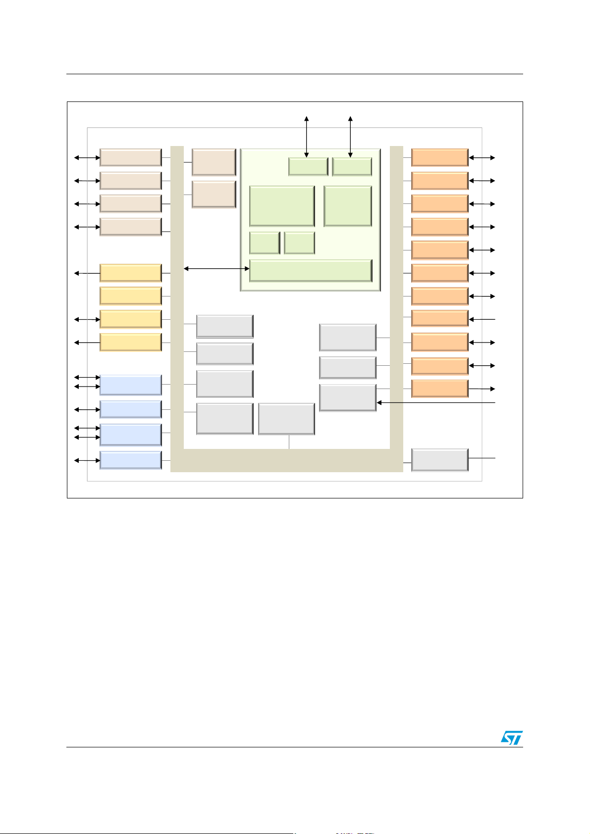
The SPEAr320S architecture is based on multiple functional blocks interacting through a
multilayer interconnection bus matrix. The switch matrix structure allows different subsystem
data flows to be executed in parallel improving the core platform efficiency. High
performance master agents are directly interconnected with the memory controller reducing
the memory access latency. The overall memory bandwidth assigned to each master port
can be programmed and optimized through an internal efficient weighted round-robin
arbitration mechanism.
The SPEAr320S device is fully backward-compatible with the previous SPEAr320 product at
both hardware and software programming levels. The extended functionality is achieved by
enhanced I/O multiplexing, preserving the same pinout and ball map, as well as by a new
software-definable configuration mode.
7. In addition, a rich set of integrated peripherals (memory interfaces, connectivity,
Doc ID 022508 Rev 1 9/97
Page 10
Description SPEAr320S
MMU
ETMI/F
ARM9EJSCore
16KB
ICache
16KB
DCache
CPU
Subsystem
DisplayCtrl
JPEGCodec
I2SAudioI/F
USB2.0Host(2x)
USB2.0Device
HMIfeatures
Highspeedconnectivity
BUSMATRIXInterconnect
GPIO
XGPIO
SSP (3x)
FastIrDA
SPP
ADC
Lowspeedconnectivity
StaticMemoryCtrl
SerialFlashI/F
ExternalMemory
I/F
Memoryinterfaces
32KB
BootROM
DDR2/LPDDR
Ctrl
DMACtrl
Cryptographic
Coprocessor
Reset&clock
Generator
System
Controller
Config Regs
(MISC)
Timers(6x)
JTAG Trace
Opt.
Battery
CAN(2x)
PWM(4x)
RS485
FastEthernet
(2x)
I2C (3x)
UART (7x)
BusInterfaces
VectoredInterrupt
Controller
DebugI/F
4KB
StaticRAM
Watchdog
SDIO/MMC
Touchscreen I/F
RTC
Figure 1. SPEAr320S architectural block diagram
10/97 Doc ID 022508 Rev 1
Page 11

SPEAr320S Device functions
2 Device functions
2.1 CPU subsystem
The core of the SPEAr320S is an ARM926EJ-S reduced instruction set computer (RISC)
processor.
Main features:
● Supports the 32-bit ARM and 16-bit Thumb instruction sets, enabling the user to trade
off between high performance and high code density. It also includes features for
efficient execution of Java byte codes.
● The ARM CPU can be clocked at a frequency up to 333 MHz and includes both an
instruction (16 KB) and a data cache (16 KB). In addition to the capability of running
any real-time operating system (RTOS) available for ARM9 processors, the
ARM926EJ-S subsystem also provides a memory management unit (MMU) that
enables to support high-level operating systems (HLLs) like Linux and Windows
Embedded Compact 7.
● Includes an embedded trace module (ETM Medium+) for real-time CPU activity tracing
and debugging. It supports 4-bit and 8-bit normal trace mode and 4-bit demultiplexed
trace mode, with normal or half-rate clock.
For detailed information, please refer to the following public documents available from the
ARM Ltd. website:
● CPU Core:
ARM9EJ-S, Technical Reference Manual, Revision: r1p2
http://infocenter.arm.com/help/topic/com.arm.doc.ddi0222b/DDI0222.pdf
● CPU Subsystem:
ARM926EJ-S, Technical Reference Manual, Revision: r0p5
http://infocenter.arm.com/help/topic/com.arm.doc.ddi0198e/DDI0198E_arm926ejs_r0p
5_trm.pdf
2.2 Internal memories (BootROM/SRAM)
SPEAr320S integrates two embedded memories:
● 32 KB ROM (BootROM), storing a factory-defined device bootstrap firmware.
● 8 KB Static RAM (SRAM), partly used by bootstrap firmware, but also available as
general-purpose memory after system startup.
The firmware in BootROM is automatically executed after SPEAr320S reset and supports
the following bootstrap modes:
● Boot from serial NOR Flash
● Boot from parallel NAND Flash
● Boot from parallel NOR Flash
● Boot from USB Device port
The BootROM firmware selects the boot mode from the boot pin settings (see Section 3.4.4:
Boot pins). A setting is also available to allow the BootROM execution to be bypassed.
Doc ID 022508 Rev 1 11/97
Page 12

Device functions SPEAr320S
The first three modes support alternate ways of locating and starting the selected operating
system or target custom software. Such modes require a second-level boot firmware to be
stored in external Flash memory. A reference code for such boot loader (called “XLoader”) is
provided by STMicroelectronics in source and binary formats for the SPEAr320S evaluation
boards. Such code must be adapted according to the specific DDR memory components
found on target customer systems.
The fourth mode can be used for installing and updating the software on external Flash
memories through a PC-based software utility provided by STMicroelectronics exploiting a
USB link between a PC and a target SPEAr320S board.
2.3 Multiport DDR controller (MPMC)
SPEAr320S integrates a high-performance controller able to manage DDR2 (double data
rate) and LPDDR (low power DDR) external dynamic memory devices.
Main features:
● Support for DDR2 up to 333 MHz (666 MT/sec)
● Support for LPDDR up to 166 MHz (333 MT/sec)
● Support for 8-/16-bit external data bus
● Support for up to 1 GByte DDR2/LPDDR memory address space
● Full initialization of memories on controller reset
● 6 independent internal ports: five of them are used to access the external memory
while one is reserved for programming the controller configuration registers
● Programmable built-in port arbitration scheme to ensure high memory bandwidth
utilization
● Fully pipelined read and write commands
● Self-refresh mode for power saving
● Integrated physical layer (PHY) and delay locked loops (DLLs) for fine tuning of the
timing parameters, maximizing the data valid windows at different frequencies
2.4 Serial NOR Flash controller (SMI)
SPEAr320S integrates a Flash memory controller able to manage serial, SPI-compatible,
NOR Flash and EEPROM external memory devices.
Main features:
● Support for up to 32 MByte external serial memory storage capacity (2 x 16 MB
addressable banks by independent chip select signals)
● SMI clock up to 50 MHz (fast read mode) or 20 MHz (normal mode), with software
configurable 7-bit prescaler
The bootstrap requires that the external serial Flash is located at bank 0 (enabled after
power-on reset). During the boot phase, a sequence of instructions is automatically sent to
bank 0. Refer to SPEAr320S reference manuals for more details.
12/97 Doc ID 022508 Rev 1
Page 13
SPEAr320S Device functions
The BootROM firmware has been tested with the following external serial memory
components:
● Micron M25P and M45P families (SPI Flash)
● Micron M95 family (SPI EEPROM), except for M95040, M95020 and M95010
● ATMEL AT25F family (SPI Flash)
● YMC Y25F family (SPI Flash)
● Microchip/SST SST25LF family (SPI Flash)
2.5 Parallel NAND Flash controller (FSMC)
SPEAr320S integrates a flexible static memory controller able to manage external parallel
NAND Flash memories.
Main features:
● 8-/16-bit external data bus; 16-bit only supported when Mode 3 (expanded automation
mode) chip configuration is selected by software.
● Support for up to 4 memory banks
● Independent timing configuration and chip select signal for each memory bank
● Fully programmable timings:
– wait states (up to 31)
– bus turnaround cycles (up to 15)
– output enable and write enable delays (up to 15)
● External asynchronous wait control
● Internal AHB bus burst transfer support to reduce Flash memory access time
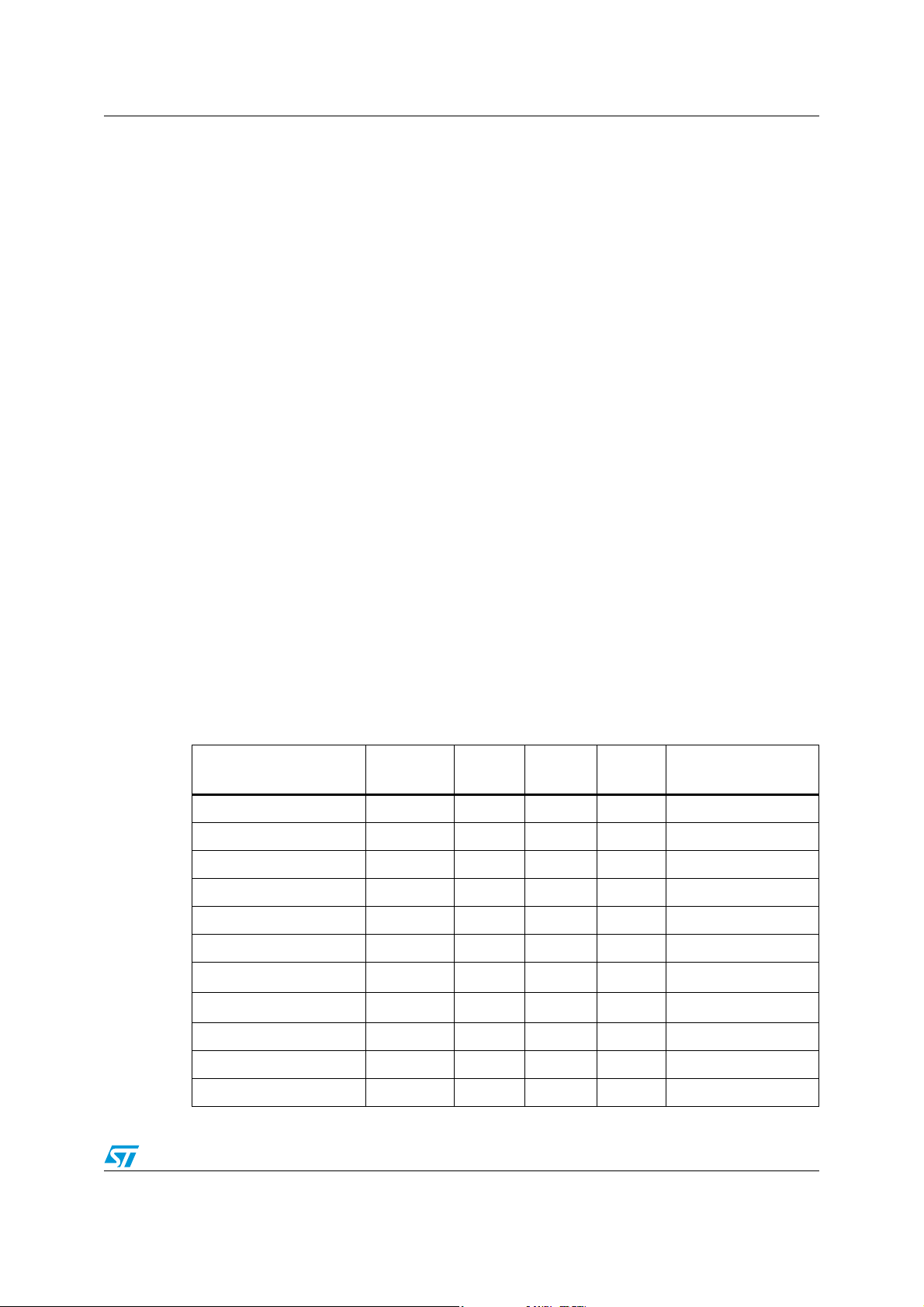
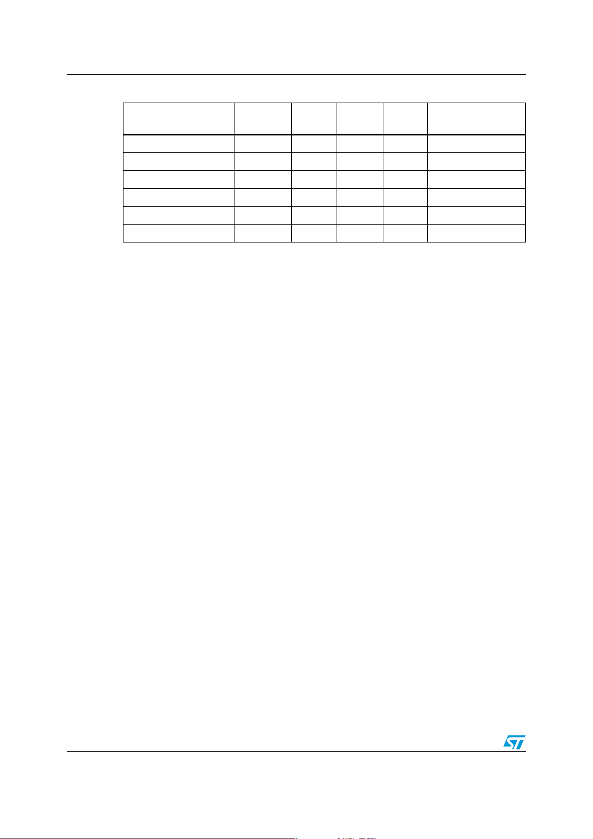
The BootROM firmware directly supports the external NAND Flash components shown in
Ta bl e 2.
Table 2. NAND Flash devices supported by the BootROM firmware
Part number Vendor Density Capacity
K9F1208V0A Samsung 64 Mb 8 MB x8 512 + 16 bytes
NAND128W3A28N6 Micron 128 Mb 16 MB x8 512 + 16 bytes
NAND256W3A2BN6 Micron 256 Mb 32 MB x8 512 + 16 bytes
KM29U256 Samsung 256 Mb 32 MB x8 512 + 16 bytes
NAND512W3A2C2A6 Micron 512 Mb 64 MB x8 512 + 16 bytes
NAND01GW3B2BN6 Micron 1 Gb 128 MB x8 2048 + 64 bytes
NAND01GW4B2AN6 Micron 1 Gb 128 MB x16 1024 words + 32 bytes
K9F1G16U0M Samsung 1 Gb 128 MB x16 1024 words + 32 bytes
NAND01GR3B Micron 1 Gb 128 MB x8 2048 + 64 bytes
NAND02GW3B2CN6 Micron 2 Gb 256 MB x8 2048 + 64 bytes
NAND02GW3A Micron 2 Gb 256 MB x8 2048 + 64 bytes
Bus
width
Page size
Doc ID 022508 Rev 1 13/97
Page 14
Device functions SPEAr320S
Table 2. NAND Flash devices supported by the BootROM firmware (continued)
Part number Vendor Density Capacity
K9F2G08V0A Samsung 2 Gb 256 MB x8 512 + 16 bytes
NAND04GW3B2BN6 Micron 4 Gb 512 MB x8 2048 + 64 bytes
K9F4G08V0A Samsung 4 Gb 512 MB x8 512 + 16 bytes
NAND08GW3B2CN6 Micron 8 Gb 1 GB x8 2048 + 64 bytes
K9K8G08V0A Samsung 8 Gb 1 GB x8 512 + 16 bytes
K9F8G08V0M Samsung 8 Gb 1 GB x8 512 + 16 bytes
2.6 External memory interface (EMI)
SPEAr320S integrates an additional external memory interface that can be used to manage
external parallel NOR Flash memories as well as FPGA devices. This interface is available
only when Mode 3 (expanded automation mode) chip configuration is selected by software.
Main features:
● 24-bit address bus
● 16-bit data bus
● 4 chip select signals
● Support for single asynchronous transfers
● Support for peripherals using Byte Lane procedure
Bus
width
Page size
The external Flash component must be in read mode at reset. Usually, this is true for most
parallel NOR devices.
2.7 USB 2.0 Host ports (UHC)
SPEAr320S provides two USB 2.0 Host ports with integrated PHYs.
Main features:
● Each port can be independently configured for high-speed mode (USB 2.0, up to
480 Mbps); in this case, the corresponding controller is programmed according to
standard EHCI specifications.
● Each port can be independently configured for full-speed mode (USB 1.1, up to
12 Mbps) or low-speed mode (USB 1.1, up to 1.5 Mbps); in this case, the
corresponding controller is programmed according to standard OHCI specifications.
● Internal 2 KB FIFO queues
● Internal DMA support
● Dedicated output control signals to manage external power switches
● Dedicated input signals to sense any over-current condition detected by external power
switches
14/97 Doc ID 022508 Rev 1
Page 15

SPEAr320S Device functions
2.8 USB 2.0 Device port (UDC)
SPEAr320S provides a USB 2.0 Device port with integrated PHY.
Main features:
● Support for all standard modes:
– high-speed mode (USB 2.0, up to 480 Mbps)
– full-speed mode (USB 1.1, up to 12 Mbps)
– low-speed mode (USB 1.1, up to 1.5 Mbps)
● Up to 16 physical endpoints, configurable as different logical endpoints
● Internal 4 KB FIFO queue (shared among all the endpoints)
● DMA mode, with descriptor-based structures in application memory
● Slave-only mode
● Support for 8-, 16- and 32-bit wide data transactions on the internal bus
● Support for USB plug detection (UPD)
2.9 Fast Ethernet ports (MII/RMII)
SPEAr320S features three multiplexed Ethernet MACs, supporting up to two ports
concurrently.
The three controllers are named:
● MII0
● RMII0
● MII1/RMII1
2.9.1 MII0 Ethernet controller
Main features:
● Media independent interface (MII) to an external PHY as defined in the IEEE 802.3u
specification
● Support for 10 and 100 Mbps data transfer rates
● Support for both full-duplex and half-duplex (CSMA/CD protocol) operating modes
● Integrated FIFO queues (4 KB RX, 2 KB TX)
● Native DMA with single-channel transmit and receive engines, providing 32-/64-/128-bit
data transfers; DMA provides ring-buffer or linked-list descriptor options.
● Programmable Ethernet frame length to support both standard and jumbo frames (with
size up to 16 KB)
● Flexible address filtering modes
● Statistics counter registers for RMON/MIB
● Support for 802.1Q VLAN tagging
● Wake-on-LAN support
● Automatic padding and CRC generation on transmitted frames
Doc ID 022508 Rev 1 15/97
Page 16

Device functions SPEAr320S
2.9.2 RMII0 and MII1/RMII1 Ethernet controllers
These functional blocks extend Ethernet capability by covering the Media independent
interface (MII) and Reduced media independent interface (RMII) standards.
They can be used in two ways:
● as a single additional MAC controller with Media independent interface (MII1)
● as two MAC controllers with Reduced media independent interface (RMII0, RMII1)
In RMII configuration, each controller has an independent set of data and control lines. The
reference clock (50
Main features:
● Compatible with IEEE Standard 802.3
● UNH tested
● 10 and 100 Mbit/s operation
● Full and half duplex operation
● Statistics counter registers for RMON/MIB
● Automatic pad and CRC generation on transmitted frames
● Automatic discard of frames received with errors
● Address checking logic supports up to four specific 48-bit addresses
● Supports promiscuous mode where all valid received frames are copied to memory
● Hash matching of unicast and multicast destination addresses
● External address matching of received frames
● Supports serial network interface operation
● Half-duplex flow control by forcing collisions on incoming frames
● Full-duplex flow control with recognition of incoming pause frames and hardware
generation of transmitted pause frames
● Support for 802.1Q VLAN tagging with recognition of incoming VLAN and priority
tagged frames
● Multiple buffers per receive and transmit frame
● Jumbo frames of up to 10240 bytes supported
MHz) is shared by the controllers.
2.10 MMC-SD card/SDIO controller
The MMC-SD card /SDIO controller conforms to the SD Host Controller Standard
Specification, version 2.0. It handles SD/SDIO protocol at transmission level by packing
data, adding cyclic redundancy check (CRC) and start/end bit as well as checking for
transaction format correctness.
The controller is designed to work with I/O cards, read-only cards and read/write cards, and
can operate either in SD mode (1-bit, 4-bit, 8-bit) or in SPI mode.
16/97 Doc ID 022508 Rev 1
Page 17

SPEAr320S Device functions
The interface is compliant to the following standards:
● SD Host Controller Standard Specification, version 2.0
● SDIO Card Specification, version 2.0
● SD Memory Card Specification Draft, version 2.0
● SD Memory Card Security Specification, version 1.01
● MMC Specification, version 3.31 and 4.2
Main features:
● Up to 100 Mbps data rate using 4 parallel data lines (SD4 bit mode)
● Up to 416 Mbps data rate using 8-bit parallel data lines (SD8 bit mode)
● DMA-based and non-DMA modes of operation
● Support for MMC Plus and MMC Mobile
● Card detection (insertion / removal)
● Card password protection
● Host clock rate variable between 0 and 48 MHz
● Multimedia card interrupt mode
● Cyclic redundancy check: CRC7 (command) and CRC16 (data integrity)
● Error correction code (ECC) support for MMC4.2 cards
● Supports for Read Wait Control and Suspend/Resume
● FIFO overrun and under-run handling by stopping SD clock
2.11 CAN 2.0 ports
SPEAr320S provides two independent CAN (controller area network) bus ports, typically
used in automotive, industrial and medical applications. For the connection to the physical
layer, an additional transceiver per port is required.
For communication on a CAN network, the controller enables to configure individual
message objects. The message objects and identifier masks for acceptance filtering of
received messages are stored in an integrated message RAM. All functions concerning the
handling of messages are implemented by a message handler. Those functions are the
acceptance filtering, the transfer of messages between the CAN core and the message
RAM, the handling of transmission requests as well as the generation of interrupts.
Main features:
● Support for CAN protocol, version 2.0 part A and B
● Transfer rate up to 1 Mbps
● Internal RAM storage for up to 16 message objects (16 x 136 bytes memory)
● Identifier mask per message object
● Maskable interrupts
● Programmable loop-back mode for self-test operation
● Disabled automatic retransmission mode for time triggered CAN applications
Doc ID 022508 Rev 1 17/97
Page 18
Device functions SPEAr320S
2.12 Asynchronous serial ports (UART)
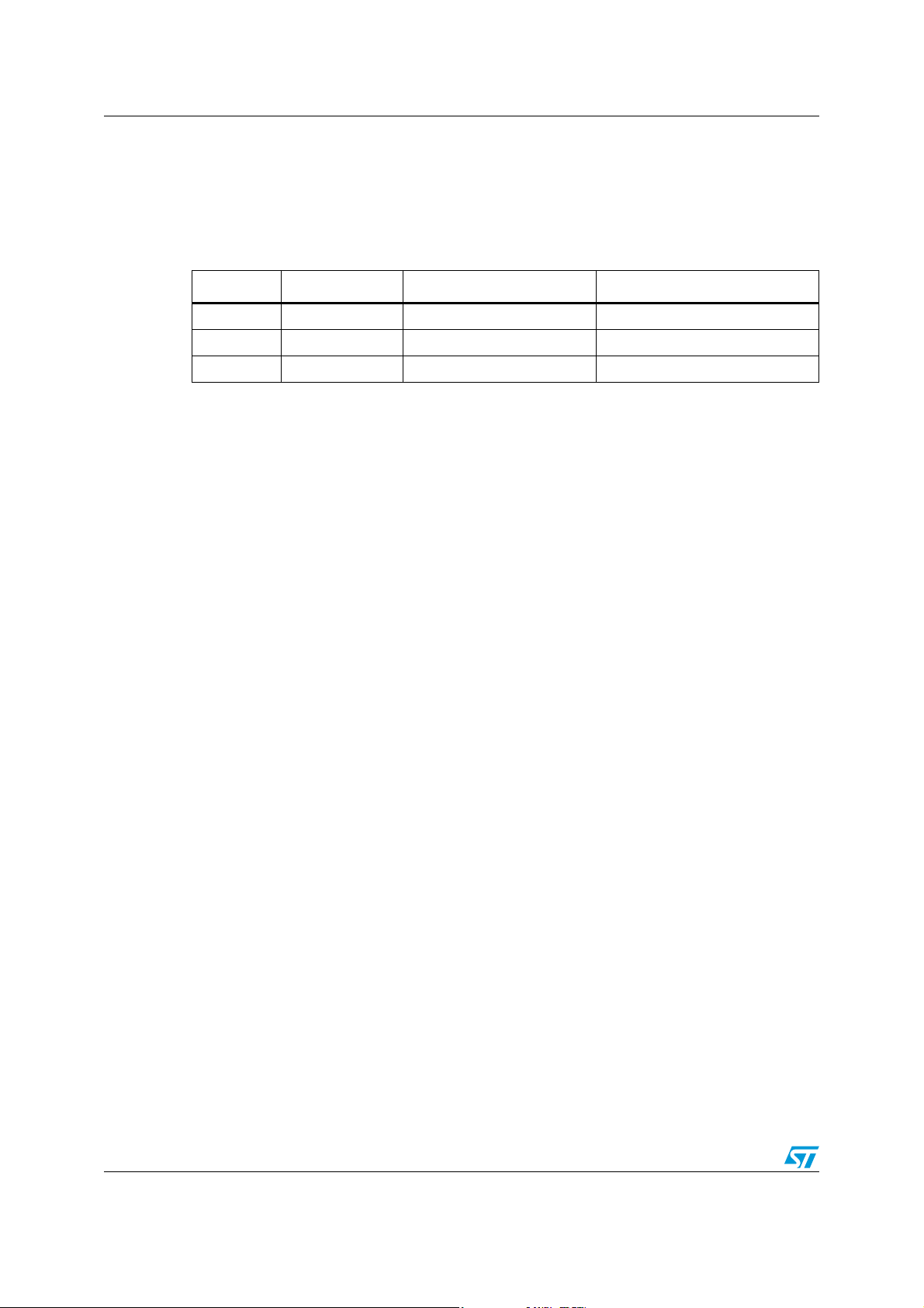
The SPEAr320S has 7 UART ports. The actual number of concurrently exploitable ports
depends on the selected chip operating mode. The different capabilities of each port are
summarized in
Table 3. SPEAr320S UART capabilities
Port Speed Hardware flow control Modem signals
UART0 Up to 3 Mbps Yes Yes (as alternate function)
UART1 Up to 7 Mbps Yes (except for Mode 1 and 2) Yes (except for Mode 1 and 2)
UART2 - 6 Up to 7 Mbps No No
Main features:
● Programmable baud rate generator
● Transmit FIFO queue (8-bit data, 16 entries) and receive FIFO queue (12-bit
data/status, 16 entries) with disabling option (1-byte buffer depth)
● Supports for DMA operation
● Hardware flow control (RTS,CTS) for some ports and configurations
● Modem control signals (DCD, DSR, DTS, RI) for some ports and configurations
● Fully programmable serial interface with following parameters:
– data bits: 5, 6, 7 or 8
– parity: even, odd, stick or none (generation and detection)
– stop bits: 1 or 2
– line break handling (generation and detection)
● Flexible interrupt handing and masking
Ta bl e 3 below.
18/97 Doc ID 022508 Rev 1
Page 19

SPEAr320S Device functions
2.13 I2C bus ports (I2C)
The SPEAr320S provides three independent I2C bus ports. Each port can be configured as
I2C bus master or slave.
Main features:
● Compliant to the I2C bus specification (Philips)
● Support for the 3 standard speeds:
– Standard (100 Kbps)
– Fast (400 kbps)
– High-speed
● Support for direct memory access (DMA)
● Clock synchronization
● Multimaster mode (bus arbitration)
● 7-bit or 10-bit addressing
● 7-bit or 10-bit combined format transfers
● Slave bulk transfer mode
● Transmit and receive buffers
● Interrupt or polled-mode operation
● Handling of bit and byte waiting at all bus speeds
● Digital filter for the received SDA and SCL lines
● Filtering out of legacy CBUS addresses
2.14 Synchronous serial ports (SSP)
SPEAr320S provides three independent synchronous serial ports. Each port can be
configured as master or slave.
Main features:
● Support for the following protocols:
– SPI (Motorola)
– Microwire (National Semiconductor)
– SSI (Texas Instruments)
● Programmable parameters:
– Clock bit rate and prescale
– Data frame size (from 4 to 16 bits)
● Separate transmit and receive FIFO queues (8 x 16-bit entries)
● Independent masking of transmit FIFO, receive FIFO, and receive overrun interrupts
● Internal loopback test mode available
● DMA interface
Doc ID 022508 Rev 1 19/97
Page 20

Device functions SPEAr320S
2.15 RS485 port (RS485)
SPEAr320S provides an additional UART port specialized for the RS485 standard.
Main features:
● Transmit FIFO queue (8-bit data, 16 entries) and receive FIFO queue (12-bit
data/status, 16 entries) with disabling option (1-byte buffer depth)
● Speed up to 7 Mbps
2.16 Fast infrared port (IrDA)
SPEAr320S provides an infrared interface compliant to the IrDA (Infrared Data Association)
standard specification. An external infrared transceiver is assumed. The Fast IrDa controller
performs the modulation and demodulation of the infrared signals as well as the wrapping of
IrDA link access protocol (IrLAP) frames.
Main features:
● Support for the following standards:
– IrDA serial infrared physical layer specification (IrPHY), version 1.3
– IrDA link access protocol (IrLAP), version 1.1
● Support for the following modes and baud rates:
– Serial infrared (SIR): 9.6 Kbps, 19.2 Kbps, 38.4 Kbps, 57.6 Kbps, 115.2 Kbps
– Medium infrared (MIR): 576 Kbps, 1152 Kbps
– Fast infrared (FIR): 4 Mbps
● Support for half-duplex infrared frame transmission and reception
● Interface compliant to all IrDA transceivers with configurable polarity of TX and RX
signals
● Integrated CRC algorithm: 16-bit (SIR, MIR), 32-bit (FIR)
● Automatic generation of preamble, start and stop flags
● RZI (return-to-zero inverted) modulation/demodulation scheme for SIR and MIR modes
● 4PPM (4-pulse position modulation) modulation/demodulation scheme for FIR mode
● Synchronization by DPLL in FIR mode
● Payload data transfer controllable by either CPU or DMA controller
● Two clock domains:
– Dedicated clock (IRDA_CLK signal) for accurate signal generation (48 MHz)
– Independent and variable clock for the bus interface (13 MHz)
2.17 Legacy IEEE 1284 parallel port (SPP)
SPEAr320S provides a parallel port (slave mode only) compliant to the legacy IEEE 1284
standard.
Main features:
● Unidirectional 8-bit data transfer from SPEAr320S slave to external host
● Additional 9th bit for parity/data/command
● Maskable interrupts for data, device reset, auto line feed
20/97 Doc ID 022508 Rev 1
Page 21

SPEAr320S Device functions
2.18 A/D converter (ADC)
SPEAr320S provides an integrated analog-to-digital converter.
Main features:
● Successive approximation conversion method
● 8 x analog input channels, ranging from 0 to 2.5 V
● 10-bit resolution
● Sampling rate up to 1 Msamples/s
● Support for 13.5-bit resolution at 8 Ksamples/s by oversampling and accumulation
● INL ± 1 LSB, DNL ± 1 LSB
● Programmable conversion speed (minimum conversion time is 1 µs)
● Programmable averaging of multiple values from 1 (no averaging) up to 128
● Programmable auto scan for all the 8 channels
2.19 General purpose I/Os (GPIO/XGPIO)
Up to 102 GPIOs are available in SPEAr320S when some embedded IPs are not needed in
the customer application (see
Section 3.4: Shared IO pins (PL_GPIOs)).
SPEAr320S provides two mechanisms:
● a basic GPIO module (called “basGPIO”): this functional block provides 6 pins, each
one programmable by software with the following features:
– direction: input (default at reset) or output
– interrupt triggering mode
● the possibility to configure and use any PL_GPIO pin as alternative to the
corresponding predefined signal purpose (called extended GPIO or “XGPIO”). XGPIOs
have the same capability of basic GPIOs, while the register programming model is
different.
Doc ID 022508 Rev 1 21/97
Page 22
Device functions SPEAr320S
2.20 LCD display controller (CLCD)
SPEAr320S has an integrated display controller able to directly interface a variety of color
and monochrome LCD panels.
Main features:
● Programmable resolution up to 1024 x 768 (XGA)
● Programmable timing parameters
● Support for TFT (thin film transistor) color displays
● Supports for STN (super twisted nematic) displays (single and dual panel) with 4- or 8-
bit interfaces
● AC bias signal for STN and data enable signal for TFT panels
● Gray scaling algorithm
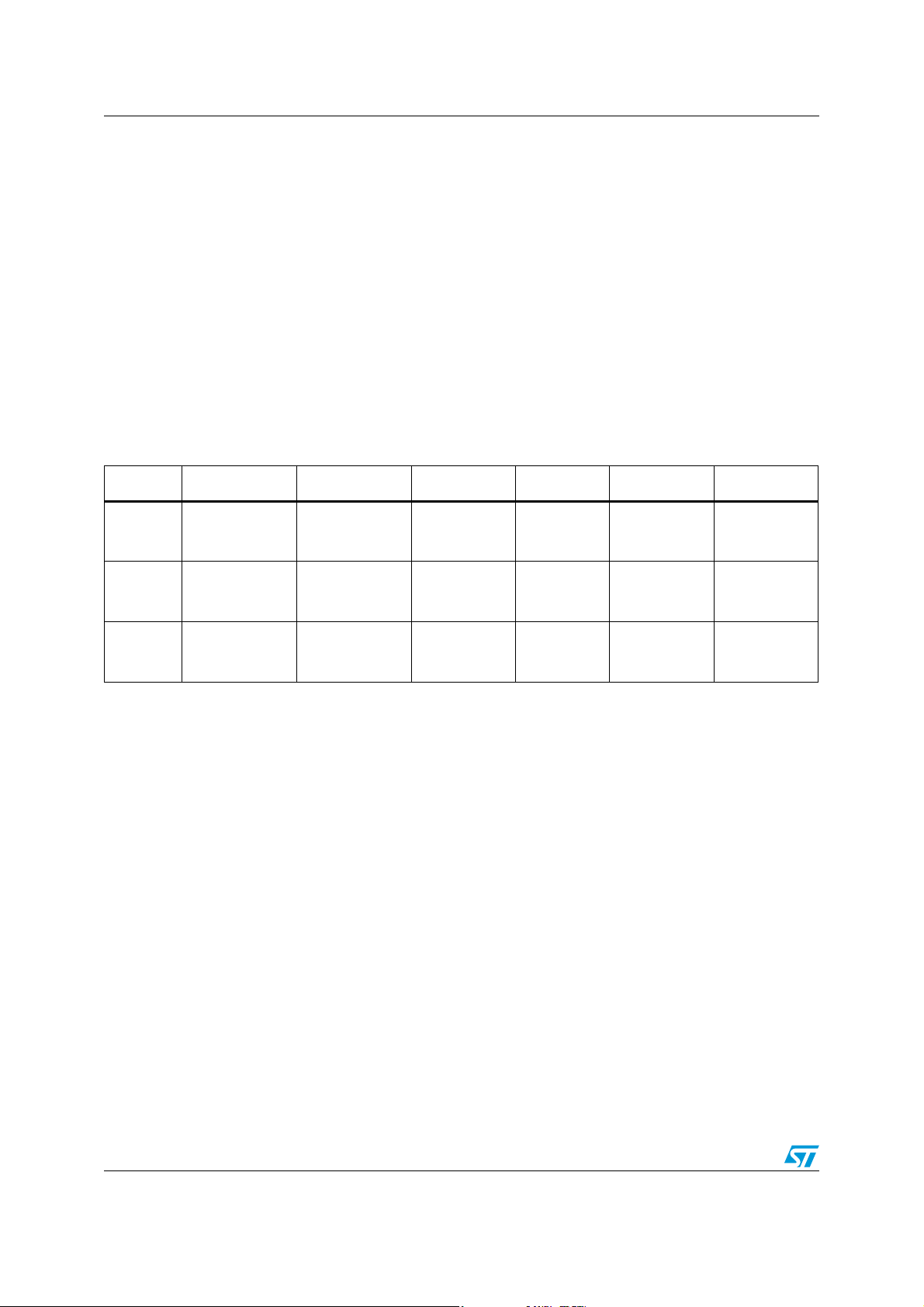
The set of supported pixel widths and formats for each display type is shown in Ta b le 4.
Table 4. Pixel widths and formats available for different display types
Display 1 bpp 2 bpp 4 bpp 8 bpp 16 bpp 24 bpp
Palette of 16
colors over
64K
Palette of 16
colors over
3375
Palette of 16
gray levels over
15
Color TFT
Color STN
Mono STN
Palette of 2
colors over 64K
Palette of 2
colors over 3375
Palette of 2 gray
levels over 15
Palette of 4
colors over 64K
Palette of 4
colors over 3375
Palette of 4 gray
levels over 15
2.21 Touchscreen interface (OUT_X)
SPEAr320S provides a toggling output signal (OUT_X) that can be connected to an external
touchscreen panel. This interface operates in combination with the A/D converter (ADC).
Two coordinates can be read by software from the ADC: one at the end of the high period
and one at the end of the low period of OUT_X signal.
Palette of
256 colors
over 64K
Palette of
256 colors
over 3375
Palette of
256 colors
over 3375
RGB 5:5:5 +
intensity
(64K colors)
RGB 4:4:4
(4096 colors)
--
RGB 8:8:8
(16M colors)
-
22/97 Doc ID 022508 Rev 1
Page 23

SPEAr320S Device functions
2.22 JPEG codec accelerator (JPGC)
SPEAr320S provides an integrated hardware accelerator for decoding and encoding
standard JPEG images.
JPEG data streams to be decoded must be compliant with the interchange format syntax
specified in the ISO/IEC 10918-1. The JFIF image file format is also supported through
header processing.
The output format for decoding (and input format for encoding) is a MCU stream, not a
conventional bitmap format like RGB. Displaying a decoded JPEG still picture would require
further steps and algorithms like color space conversion and scaling.
Main features:
● Compliance with the baseline JPEG standard (ISO/IEC 10918-1)
● Single-clock per pixel encoding/decoding
● Support for up to four channels of component color
● 8-bit/channel pixel depths
● Programmable quantization tables (up to four)
● Programmable Huffman tables (two AC and two DC)
● Programmable minimum coded unit (MCU)
● Configurable JPEG header processing
● Support for restart marker insertion
● Use of two DMA channels and two 8 x 32-bit FIFOs (local to the JPEG) for efficient
transferring and buffering of encoded/decoded data from/to the Codec core.
2.23 Digital audio port (I2S)
The SPEAr320S integrates a digital audio port compliant to standard I2S (Philips)
specifications.
Main features:
● I2S master mode
● Stereo (2.0) playback and recording
● Support for standard sampling rates (8, 16, 32, 44.1, 48, 96, 192 kHz); the clock input is
24 MHz, so the rate precision depends on the chosen rate and divider.
● Support of a range of audio samples: 12 / 16 / 20 / 24/ 32 bits
● Programmable thresholds for internal FIFO queues
● Capability of using DMA transfer
2.24 Cryptographic co-processor (C3)
SPEAr320S provides an embedded cryptographic co-processor (C3). C3 is a high-
performance instruction-driven DMA-based engine that can be used to accelerate the
processing of security algorithms.
After its initial configuration by the main CPU, it runs in a completely autonomous way (DMA
data in, data processing, DMA data out), until the completion of all the requested operations.
C3 firmware is fetched from system memory.
Doc ID 022508 Rev 1 23/97
Page 24

Device functions SPEAr320S
Main features:
● Supported cryptographic algorithms:
– Advanced encryption standard (AES) cipher in ECB, CBC, CTR modes
– Data encryption standard (DES) cipher in ECB and CBC modes
– SHA-1, HMAC-SHA-1, MD5, HMAC-MD5 digests
● Hardware chaining of cryptographic stages for optimized data flow when multiple
algorithms are required to process the same set of data (for example, encryption and
hashing on the fly)
2.25 System controller (SYSCTR)
The system controller provides an interface for controlling the operation of the overall
system.
Main features:
● Power saving system mode control
● Crystal oscillator and PLL control
● Configuration of system response to interrupts
● Reset status capture and soft reset generation
● Watchdog and timer module clock enable
Using three mode control bits, the system controller switches the SPEAr320S to any of the
four different modes: DOZE, SLEEP, SLOW and NORMAL.
● SLEEP mode: in this mode, the system clocks, HCLK and CLK, are disabled and the
system controller clock, SCLK, is driven by a low-speed oscillator (nominally
32768 Hz). When either a FIQ or an IRQ interrupt is generated (through the VIC), the
system enters DOZE mode. Additionally, the operating mode setting in the system
control register automatically changes from SLEEP to DOZE.
● DOZE mode: in this mode, the system clocks, HCLK and CLK, and the system
controller clock are driven by a low-speed oscillator. The system controller moves into
SLEEP mode from DOZE mode only when none of the mode control bits are set and
the processor is in wait-for-interrupt state. If SLOW mode or NORMAL mode is
required, the system moves into the XTAL control transition state to initialize the crystal
oscillator.
● SLOW mode: during this mode, both the system clocks and the system controller clock
are driven by the crystal oscillator. If NORMAL mode is selected, the system goes into
the “PLL control” transition state. If neither the SLOW nor the NORMAL mode control
bits are set, the system goes into the “Switch from XTAL” transition state.
● NORMAL mode: in NORMAL mode, both the system clocks and the system controller
clock are driven by the PLL output. If the NORMAL mode control bit is not set, then the
system goes into the “Switch from PLL” transition state.
24/97 Doc ID 022508 Rev 1
Page 25

SPEAr320S Device functions
2.25.1 Reset and clock generator
The reset and clock generator is a fully programmable block that generates all the clocks
necessary to the chip.
The default operating clock frequencies are:
● Clock @ 333 MHz for the CPU.
● Clock @ 166 MHz for AHB bus and AHB peripherals.
● Clock @ 83 MHz for, APB bus and APB peripherals.
● Clock @ 333 MHz for DDR memory interface.
The default values give the maximum allowed clock frequencies. The clock frequencies are
fully programmable through dedicated registers.
The reset and clock generator consists of 2 main parts:
● a multiclock generator block
● two internal PLLs
The multiclock generator block receives a reference signal (which is usually delivered by the
PLL) and generates all clocks for SPEAr320S IPs according to dedicated programmable
registers.
Each PLL uses an oscillator input of 24 MHz to generate a clock signal at a frequency
corresponding at the highest of the group. This is the reference signal used by the multiclock
generator block to obtain all the other requested clocks for the group. Its main feature is the
electromagnetic interference reduction capability.
You can set up the PLL in order to modulate the VCO with a triangular wave. The resulting
signal has a spectrum (and power) spread over a small programmable range of frequencies
centered on F0 (the VCO frequency), obtaining minimum electromagnetic emissions. This
method replaces all the other traditional methods of EMI reduction, such as filtering, ferrite
beads, chokes, adding power layers and ground planes to PCBs, metal shielding and so on.
This offers important cost savings.
In sleep mode, SPEAr320S runs with the PLL disabled, so the available frequency is
24
MHz or a sub-multiple (/2, /4, /8).
2.26 Vectored interrupt controller (VIC)
SPEAr320S integrates a vectored interrupt controller which provides a software interface to
the interrupt system. In any system with an interrupt controller, the software has to
determine the source that requests service and where its service routine is loaded. The VIC
inside SPEAr320S does both of these in hardware. It supplies the starting address, or vector
address, of the service routine corresponding to the highest priority requesting interrupt
source.
As in any ARM9-based system, two levels of interrupts are available:
● fast interrupt requests (FIQ), for fast, low latency interrupt handling
● normal interrupt requests (IRQ), for more general interrupts
The interrupt inputs must be level sensitive, active HIGH, and held asserted until the
interrupt service routine clears the interrupt. Edge-triggered interrupts are not compatible.
The interrupt inputs do not have to be synchronous to HCLK. The VIC does not handle
interrupt sources with transient behavior. For example, an interrupt is asserted and then de-
Doc ID 022508 Rev 1 25/97
Page 26

Device functions SPEAr320S
asserted before software can clear the interrupt source. In this case, the CPU acknowledges
the interrupt and obtains the vectored address for the interrupt from the VIC, assuming that
no other interrupt has occurred to overwrite the vectored address. However, when a
transient interrupt occurs, the priority logic of the VIC is not set, and lower priority interrupts
can interrupt the transient interrupt service routine, assuming interrupt nesting is permitted.
There are 32 interrupt lines. The VIC uses a bit position for each different interrupt source.
The software can control each request line to generate software interrupts. There are 16
vectored interrupts. These interrupts can only generate an IRQ interrupt. The vectored and
non-vectored IRQ interrupts provide an address for an interrupt service routine (ISR). The
FIQ interrupt has the highest priority, followed by interrupt vector 0 to interrupt vector 15.
Non-vectored IRQ interrupts have the lowest priority.
The specific interrupt map for the SPEAr320S device is documented in the companion
reference manuals.
2.27 Watchdog timer (WDT)
The ARM watchdog module consists of a 32-bit down counter with a programmable time-out
interval that has the capability to generate an interrupt and a reset signal on timing out. The
watchdog module is intended to be used to apply a reset to a system in the event of a
software failure.
2.28 Real-time clock (RTC)
The real-time clock provides an 1-second resolution clock. This keeps time when the system
is inactive and can be used to wake the system up when a programmed alarm time is
reached. RTC has a clock trimming feature to compensate for the accuracy of the 32.768
kHz crystal and a secured time update.
Main features:
● Time-of-day clock in 24 hour mode
● Calendar
● Alarm capability
● Isolation mode, allowing RTC to work even if power is not supplied to the rest of the
device.
2.29 DMA controller (DMAC)
SPEAr320S provides one DMA controller.
Main features:
● Able to service up to 8 independent DMA channels for serial data transfers between
single source and destination (for instance, memory-to-memory, memory-to-peripheral,
peripheral to- memory, and peripheral-to-peripheral).
● Each DMA channel can support a unidirectional transfer, with internal four-word FIFO
per channel.
26/97 Doc ID 022508 Rev 1
Page 27

SPEAr320S Device functions
2.30 General purpose timers (GPT)
SPEAr320S provides 6 general purpose timers.
Main features:
● Each timer provides a programmable 16-bit counter and a dedicated 4-bit prescaler
able to perform a clock division by 1 up to 256 (different input frequencies can be
chosen through configuration registers, in the range from 3.96 Hz to 48 MHz)
● Operating modes:
– Auto-reload mode: when a software-defined value is reached, an interrupt is
triggered and the counter automatically restarts from zero
– Single-shot mode: when a software-defined value is reached, an interrupt is
triggered, the counter is stopped and the timer is disabled
● Capture capability (only for 4 timers)
2.31 Pulse width modulators (PWM)
SPEAr320S integrates 4 PWM (pulse width modulation) signal generators.
Main features:
● Prescaler to define the input clock frequency to each timer
● Programmable duty cycle from 0% to 100%
● Programmable pulse length
Doc ID 022508 Rev 1 27/97
Page 28
Pin description SPEAr320S
3 Pin description
This chapter provides a full description of the ball characteristics and the signal multiplexing
of SPEAr320S device.
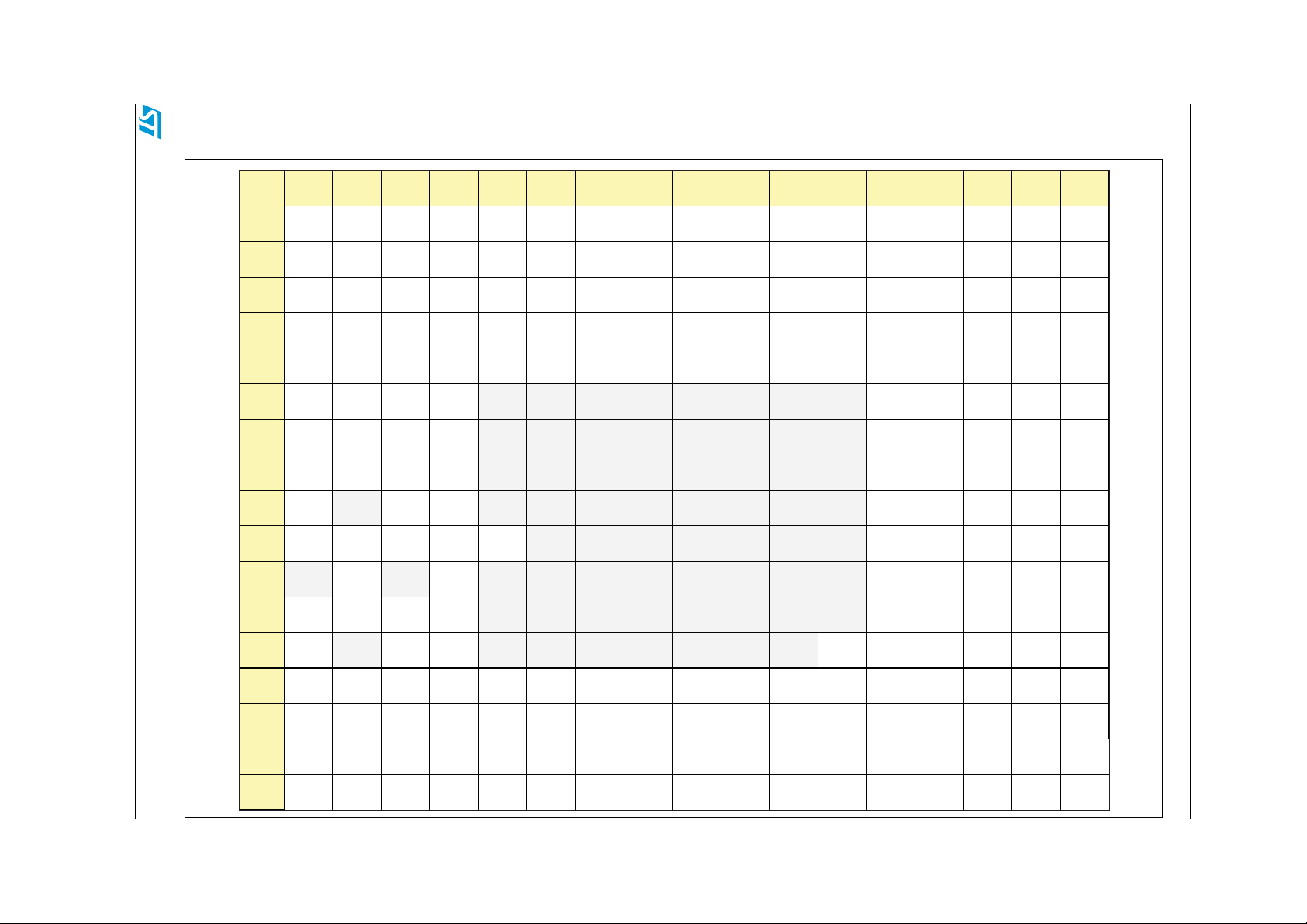
Section 3.1 shows the pin/ball map of SPEAr320S.
Section 3.2 lists the required external components to connect.
Section 3.3 describes some dedicated pins, such as:
● Clock, reset and 3V3 comparator pins
● Power supply pins
● Debug pins
● Non-multiplexed pins
Section 3.4 provides a complete description of the shared IO pins (PL_GPIOs) and their
configuration modes, as well as detailed information on all multiplexed signals, grouped by
IP.
Section 3.5 explains the available debug modes.
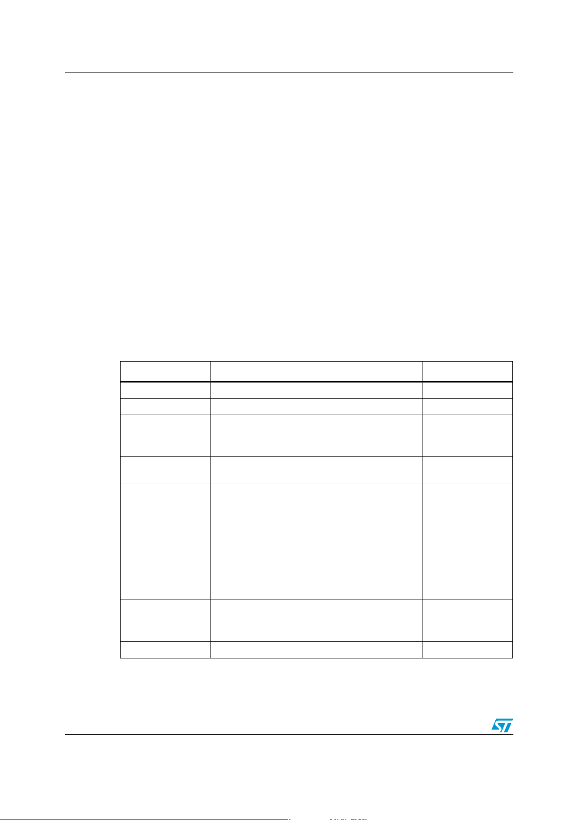
The following table defines the table headers and abbreviations used in this chapter.
Table 5. Headers/abbreviations
Header Description Abbreviations
Group Grouping of signals of the same type/functional block. –
Signal name Name of signal multiplexed on each ball. –
I= Input
Direction (Dir.) Indicates the direction of the signal.
PL_GPIO_# /Ball
Configuration mode
Pin type Pad type information
Val ue Indicates the electrical value on the ball. –
PL_GPIO and ball number associated with each
signal on the package.
Indicates the available configuration mode among the
following ones:
– Mode 1
– Mode 2
– Mode 3
– Mode 4
– Alternate function
– Extended mode
See Section 3.4.2 for the description of each mode.
O= Output
IO= Input/output
–
–
PU= Pull Up
PD= Pull Down
GND= Ground
28/97 Doc ID 022508 Rev 1
Page 29
3.1 Pin/ball map
_
_
_
DIGITAL_
REXT
digital_vdde
3v3
gnd gnd gnd gnd gnd gnd vdd PL_GPIO _87 PL_GPIO_90 PL_GPIO_91 PL_GPIO _92 PL_GPIO_93
H
vdd gnd gnd gnd gnd gnd gnd v dd PL_G PIO_94PL_GPIO_95PL_GPIO_96PL_GPIO_97PL_CLK4
J
gnd
vdd gnd gnd gnd gnd gnd gnd digital_vdde
3v3
DDR2_EN BOOT_SEL T EST_4 PL_CLK3 PL_CLK2
K
USB_TXR
TUNE
gnd gnd gnd gnd gnd gnd digital_vdde
3v3
TEST_3 TEST_2 TEST_1 TEST_0 PL_CLK1
L
gnd
gnd
G
_
_
dith_vdd2v5 DDR_v dde1v8 vdd vdd gnd gnd gnd vdd digital_vdde
3v3
SMI_DATAIN
SMI_DATAO UT
SMI_CS_0 SMI_CS_1 MRESET
N
gnd
ADC_VREF P AIN_4 AIN_3 AIN _2
R
MCLK_VDD MCLK_
VDD2V5
P
DDR_MEM_
WE
DDR_MEM_
DQ_8
U
DDR_MEM_
DQ_10
Figure 2. SPEAr320S pin/ball map
123 45678 9 10111213 14 15 16 17
PL_GPIO_13 PL_GPIO _14 PL_GPIO_19 PL_GPIO_23 PL_GPIO _26 PL_GPIO_28 PL_G PIO_29 PL_GPIO_38 PL_GPIO_39 PL_GPIO _44 PL_GPIO_46 PL_GPIO_50 PL_G PIO_55 PL_GPIO_60 PL_GPIO_62 PL_GPIO_69 PL_G PIO_73
A
PL_GPIO_6 PL_GPIO_9 PL_GPIO _15 PL_GPIO_20 PL_GPIO_24 PL_G PIO_27 PL_GPIO_30 PL_GPIO_37 PL_GPIO_40 PL_GPIO _45 PL_GPIO_48 PL_GPIO_52 PL_G PIO_59 PL_GPIO _65 PL_GPIO _68 PL_GPIO_72 PL_G PIO_77
B
PL_GPIO_4 PL_GPIO_8 PL_GPIO _10 PL_GPIO_17 PL_GPIO_21 PL_G PIO_25 PL_GPIO_31PL_GPIO_36 PL_GPIO_41 PL_G PIO_47 PL_GPIO_49 PL_GPIO_56 PL_GPIO_63 PL_G PIO_67 PL_ GPIO_70 PL_GPIO _74 PL_G PIO_81
C
PL_GPIO_3 PL_GPIO_5 PL_G PIO_7 PL_GPIO_12 PL_GPIO_18 PL_G PIO_22 PL_GPIO_32 PL_GPIO_35 PL_GPIO_42 PL_GPIO_51 PL_GPIO_53 PL_GPIO _58 PL_GPIO_64 PL_GPIO_71 PL_G PIO_78 PL_GPIO _80PL_GPIO_84
D
RTC_XO RTC_XI PL_GPIO_1 PL_GPIO_2 PL_GPIO_11 PL_GPIO_16 PL_GPIO _33 PL_GPIO_34 PL_GPIO_43 PL_G PIO_54 PL_GPIO_57 PL_GPIO_61 PL_GPIO_66 PL_GPIO _75 PL_GPIO_82PL_GPIO_83 PL _GPIO_86
E
SPEAr320S Pin description
Doc ID 022508 Rev 1 29/97
RTC_vdd1v 5 RTC_gnd PL_GPIO_0
F
DITH _pll_vss
G
ana
USB_HOST1_DPUSB_HOST1_DMUSB_HOST1_
USB_HOST1_
vdd3v3
USB_HOST0_DPUSB_HOST0_DMUSB_HOST1_
USB_DEVICE
M
DP
USB_DEVICE
_vdd2v5
MCLK_XI MCLK_XO MCLK_G ND
P
DDR_MEM_
T
ADDR_1
DDR_MEM_
ADDR_2
DITH _pll_vd d
ana
USB_HOST0_
vdd2v5
USB_DEVICE
DM
DDR_MEM_
ADDR_0
DDR_MEM_
ADDR_3
USB_DEVICE
VBUS
VBUS
USB_HOST0_
VBUS
vdd2v5
USB_HOST1_
HOST0_
DEVICE_
Dvdd1v2
USB_DEVICE
_vdd3v3
MCLK_
GNDSUB
DDR_MEM_
ODT_0
DDR_MEM_
ADDR_4
DIGITAL_
GNDBG
COMP
USB_HOST0_
OVERCUR
USB_HOST1_
OVERCUR
USB_HOST0_
vdd3v3
USB_ANALO
TEST
dith_vss2v5 DDR_v dde1v8 DDR_vdde1v8 D DR_vdde1v8 DDR_vdde1v 8DDR_v dde1v8 DDR_vdde1v 8D DR_vdde1v8 ADC_agnd ADC_avdd ADC_VREFN AIN_1 AIN_0 SMI_CLK
DDR_MEM_
COMP2V5_
DDR_MEM_
COMP2V5_
GNDBGCOM
DDR_MEM_
ODT_1
DDR_MEM_
ADDR_5
digital_vdde
3v3
gnd gnd gnd gnd gnd gnd vdd digital_vdde
DDR_MEM_
ADDR_9
DDR_MEM_
ADDR_8
DDR_MEM_
ADDR_7
DDR_MEM_
ADDR_6
digital_vdde
3v3
DDR_MEM_
ADDR_10
DDR_MEM_
ADDR_11
DDR_MEM_
ADDR_12
DDR_MEM_
ADDR_13
digital_vdde
3v3
DDR_MEM_
BA_0
DDR_MEM_
ADDR_14
DDR_MEM_
CLKEN
vdd vdd digital_vdd e
DDR_MEM_
BA_1
DDR_MEM_
BA_2
DDR_MEM_
CAS
DDR_MEM_
RAS
DDR_MEM_
CS_0
DDR_MEM_
CS_1
DDR_MEM_
CLKP
DDR_MEM_
CLKN
3v3
DDR_MEM_
VREF
DDR_MEM_
GATE_OPEN
_0
nDDR_MEM_
DQS_0
DDR_MEM_
DQS_0
digital_vdde
3v3
DDR_MEM_
DQ_0
DDR_MEM_
DQ_1
DDR_MEM_
DQ_2
DDR_MEM_
DQ_3
digital_vdde
3v3
3v3
DDR_MEM_
DQ_6
DDR_MEM_
DQ_5
DDR_MEM_
DQ_4
DDR_MEM_
DM_0
PL_GPIO_76 PL_GPIO _79 PL_GPIO_85PL_GPIO_88 PL _GPIO_89
TMS TDI TDO nTRSTTCK
DDR_MEM_
DQ_7
DDR_MEM_
DQ_15
DDR_MEM_
DQ_14
DDR_MEM_
DQ_13
DDR_MEM_
GATE_OPEN
_1
DDR_MEM_
DM_1
DDR_MEM_
DQ_12
AIN_7 AIN_ 6 AIN_5
nDDR_MEM_
DQS_1
DDR_MEM_
DQS_1
DDR_MEM_
DQ_9
DDR_MEM_
DQ_11
Page 30
Pin description SPEAr320S
3.2 Required external components
Some pads require the use of an external component. Please follow the instructions below
to ensure the proper functioning of the device:
1. DDR_COMP_1V8: place an external 121 kΩ resistor between ball P4 and ball R4
2. USB_TX_RTUNE: connect an external 43.2 Ω pull-down resistor to ball K5
3. DIGITAL_REXT: place an external 121 kΩ resistor between ball G4 and ball F4
4. DITH_VDD_2V5: add a ferrite bead to ball M4
3.3 Dedicated pins description
3.3.1 Clock, reset and 3V3 comparator pins
Table 6. MCLK, RTC, Reset and 3.3 V comparator pins description
Group Signal name Description Dir. Pin type Ball
Master clock
(MCLK)
Real-time clock
(RTC)
Reset MRESET Main reset I
3.3 V
comparator
MCLK_XI 24 MHz (typical) crystal in I
Oscillator 2.5 V capable
MCLK_XO 24 MHz (typical) crystal out O P2
RTC_XI 32 kHz crystal in I
Oscillator 1V5 capable
RTC_XO 32 kHz crystal out O E1
TTL Schmitt trigger input
buffer, 3.3 V tolerant
DIGITAL_REXT Configuration O Analog, 3.3 V capable G4
DIGITAL_GNDBGCOMP Power Power Power F4
P1
E2
M17
30/97 Doc ID 022508 Rev 1
Page 31
SPEAr320S Pin description
3.3.2 Power supply pins
Table 7. Power supply pins description
Group Signal name Value Ball
G6 G7 G8 G9 G10 G11 H6 H7
Digital ground
GND
H8 H9 H10 H11 J6 J7 J8 J9 J10
J11 K6 K7 K8 K9 K10 K11 L6 L7
0 V
USB_HOST1_HOST0_DEVICE_DVSS L5
RTC_GND
DITH_PLL_VSS_ANA G1
USB_HOST1_VSSA J2
USB_HOST0_VSSA L1
USB_COMMON_VSSAC L3
Analog ground
0 V
USB_DEVICE_VSSA N2
DITH_VSS2V5 N4
MCLK_GND P3
MCLK_GNDSUB R3
ADC_AGND N12
IO DIGITAL_VDDE3V3 3.3 V
F5 F6 F7 F10 F11 F12 G5 J12
L8 L9 L10 M8 M9 M10
F2
K12 L12 M12
Core VDD 1.2 V
F8 F9 G12 H5 H12 J5 L11 M6
M7 M11
USB_HOST0_VDD2V5 2.5 V L2
USB Host0 PHY
USB_HOST0_VDD3V3 3.3 V K4
USB_HOST1_VDD2V5 2.5 V K3
USB Host1 PHY
USB_HOST1_VDD3V3 3.3 V J1
USB_DEVICE_VDD2V5 2.5 V N1
USB Device PHY
USB_DEVICE_VDD3V3 3.3 V N3
USB_HOST1_HOST0_DEVICE_DVDD1V2 1.2 V M3
MCLK_VDD 1.2 V R1
OSCI (MCLK)
MCLK_VDD2V5 2.5 V R2
PLL1 DITH_PLL_VDD_ANA 2.5 V G2
PLL2 DITH_VDD_2V5 2.5 V M4
DDR IO DDR_VDDE1V8 1.8 V M5 N5 N6 N7 N8 N9 N10 N11
ADC ADC_AVDD 2.5 V N13
OSCI (RTC) RTC_VDD1V5 1.5 V F1
Note: All the VDD 2V5 power supplies are analog VDD.
Doc ID 022508 Rev 1 31/97
Page 32
Pin description SPEAr320S
3.3.3 Debug pins
Table 8. Debug pins description
Signal name Description Dir. Pin type Ball
TEST_0
K16
TEST_1 K15
TEST_2 K14
TEST_3 K13
Test configuration ports. For functional
mode, they have to be set to zero.
TTL input buffer, 3.3 V tolerant,
I
PD
TEST_4 J15
BOOT_SEL Reserved, to be fixed at high level J14
nTRST Test reset input I
TDO Test data output O
TCK Test clock I
TDI Test data input I L14
TTL Schmitt trigger input
buffer, 3.3 V tolerant, PU
TTL output buffer, 3.3 V
capable 4 mA
TTL Schmitt trigger input
buffer, 3.3 V tolerant, PU
L16
L15
L17
TMS Test mode select I L13
Note: See also Section 3.5: PL_GPIO pin sharing for debug modes.
3.3.4 Non-multiplexed pins
Table 9. SMI pins description
SMI_DATAIN Serial Flash input data I TTL Input Buffer 3.3 V tolerant, PU M13
SMI_DATAOUT Serial Flash output data O
SMI_CLK Serial Flash clock IO N17
SMI_CS_0
SMI_CS_1 M16
Signal name Description Dir. Pin type Ball
M14
TTL output buffer 3.3 V capable 4 mA
M15
Serial Flash chip select O
32/97 Doc ID 022508 Rev 1
Page 33
SPEAr320S Pin description
Table 10. USB pins description
Group Signal name Description Dir. Pin type Ball
USB
Device
USB_DEVICE_DP USB Device D+
USB_DEVICE_DM USB Device D- M2
USB_DEVICE_VBUS USB Device VBUS I
USB_HOST1_DP USB Host1 D+
USB_HOST1_DM USB Host1 D- H2
USB_HOST1_VBUS USB Host1 VBUS O
USB_HOST1_OVERCUR USB Host1 Over-Current I
Bidirectional analog buffer
IO
5 V tolerant
TTL input buffer 3.3 V
tolerant, PD
Bidirectional analog buffer
IO
5 V tolerant
TTL output buffer 3.3 V
capable, 4 mA
TTL input buffer 3.3 V
tolerant, PD
USB Host
USB_HOST0_DP USB Host0 D+
USB_HOST0_DM USB Host0 D- K2
USB_HOST0_VBUS USB Host0 VBUS O
USB_HOST0_OVERCUR USB Host0 Over-current I
Bidirectional analog buffer
IO
5 V tolerant
TTL output buffer 3.3 V
capable, 4 mA
TTL Input Buffer 3.3 V
tolerant, PD
USB_TXRTUNE Reference resistor O Analog K5
USB
USB_ANALOG_TEST Analog test output O Analog L4
M1
G3
H1
H3
J4
K1
J3
H4
Table 11. ADC pins description
Signal name Description Dir. Pin type Ball
AIN_0
N16
AIN_1 N15
AIN_2 P17
AIN_3 P16
ADC analog input channel
AIN_4 P15
I Analog buffer 2.5 V tolerant
AIN_5 R17
AIN_6 R16
AIN_7 R15
ADC_VREFN ADC negative voltage reference N14
ADC_VREFP ADC positive voltage reference P14
Doc ID 022508 Rev 1 33/97
Page 34
Pin description SPEAr320S
Table 12. DDR pins description
Signal name Description Dir. Pin type Ball
DDR_MEM_ADD_0
DDR_MEM_ADD_1 T1
DDR_MEM_ADD_2 U1
DDR_MEM_ADD_3 U2
DDR_MEM_ADD_4 U3
DDR_MEM_ADD_5 U4
DDR_MEM_ADD_6 U5
DDR_MEM_ADD_7 T5
DDR_MEM_ADD_8 R5
DDR_MEM_ADD_9 P5
DDR_MEM_ADD_10 P6
DDR_MEM_ADD_11 R6
DDR_MEM_ADD_12 T6
DDR_MEM_ADD_13 U6
DDR_MEM_ADD_14 R7
DDR_MEM_BA_0
DDR_MEM_BA_1 P8
DDR_MEM_BA_2 R8
Address Line O
SSTL_2/SSTL_18
Bank select O
T2
P7
DDR_MEM_RAS Row address strobe O U8
DDR_MEM_CAS Column address strobe O T8
DDR_MEM_WE Write enable O T7
DDR_MEM_CLKEN Clock enable O U7
DDR_MEM_CLKP
DDR_MEM_CLKN U9
DDR_MEM_CS_0
DDR_MEM_CS_1 R9
DDR_MEM_ODT_0
DDR_MEM_ODT_1 T4
Differential clock O
Chip select O
On-die termination enable
lines
Differential SSTL_2/
SSTL_18
SSTL_2/ SSTL_18
IO
T9
P9
T3
34/97 Doc ID 022508 Rev 1
Page 35
SPEAr320S Pin description
Table 12. DDR pins description (continued)
Signal name Description Dir. Pin type Ball
DDR_MEM_DQ_0
DDR_MEM_DQ_1 R11
DDR_MEM_DQ_2 T11
DDR_MEM_DQ_3 U11
DDR_MEM_DQ_4 T12
DDR_MEM_DQ_5 R12
DDR_MEM_DQ_6 P12
DDR_MEM_DQ_7 P13
DDR_MEM_DQS_0
nDDR_MEM_DQS_0 T10
DDR_MEM_DM_0 Lower data mask O
DDR_MEM_GATE_OPEN_0 Lower gate open IO R10
DDR_MEM_DQ_8
DDR_MEM_DQ_9 T16
DDR_MEM_DQ_10 U17
DDR_MEM_DQ_11 U16
DDR_MEM_DQ_12 U14
DDR_MEM_DQ_13 U13
Data lines
(lower byte)
Lower data strobe O
Data lines
(upper byte)
IO SSTL_2/ SSTL_18
IO
Differential SSTL_2/
SSTL_18
SSTL_2/ SSTL_18
P11
U10
U12
T17
DDR_MEM_DQ_14 T13
DDR_MEM_DQ_15 R13
DDR_MEM_DQS_1
nDDR_MEM_DQS_1 T15
DDR_MEM_DM_1 Upper data mask
DDR_MEM_GATE_OPEN_1 Upper gate open R14
DDR_MEM_VREF Reference voltage I Analog P10
DDR_MEM_COMP2V5_GNDBGCOMP
DDR_MEM_COMP2V5_REXT External resistor Power Analog P4
DDR2_EN Configuration I
Upper data strobe IO
Return for external
resistors
Power Power R4
Differential SSTL_2/
SSTL_18
IO SSTL_2/ SSTL_18
TTL Input Buffer 3.3 V
Tol e r a n t , P U
U15
T14
J13
Doc ID 022508 Rev 1 35/97
Page 36
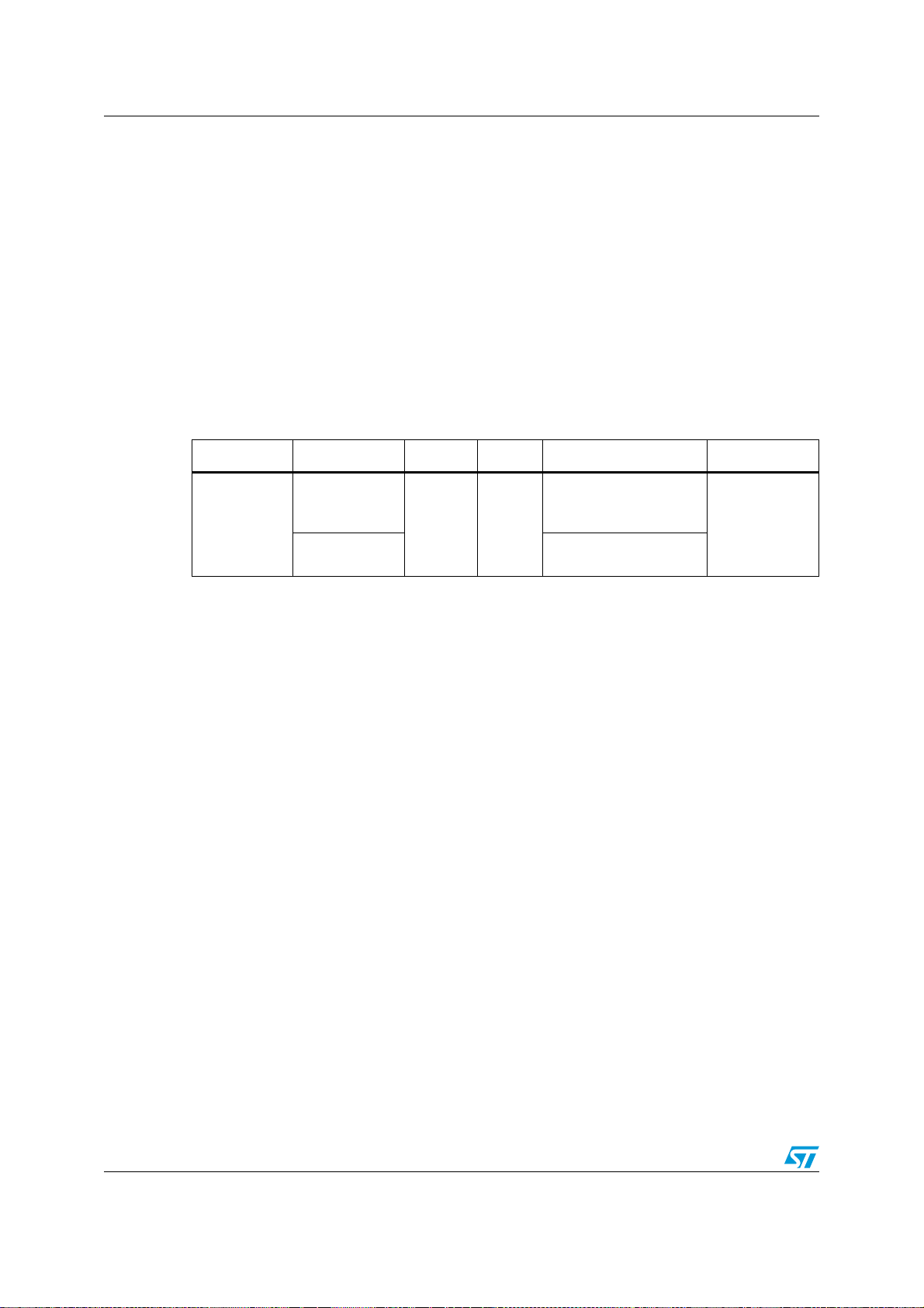
Pin description SPEAr320S
3.4 Shared IO pins (PL_GPIOs)
The 98 PL_GPIO and 4 PL_CLK pins have the following characteristics:
● Output buffer: TTL 3.3 V capable up to 10 mA
● Input buffer: TTL, 3.3 V tolerant, selectable internal pull up/pull down (PU/PD)
The PL_GPIOs can be configured in different modes. This allows SPEAr320S to be tailored
for use in various applications like:
● Metering concentrators
● Large power supply controllers
● Small printers
3.4.1 PL_GPIO pins description
Table 13. PL_GPIO pins description
Group Signal name Ball Dir. Description Pin type
General purpose IO or
multiplexed pins (see
Table 15)
IO
Programmable logic
external clocks
(See the
introduction of
Section 3.4 here
above)
PL_GPIOs
PL_GPIO_97...
PL_GPIO_0
PL_CLK1...
PL_CLK4
(See the
Table 15)
3.4.2 Configuration modes
This section describes the main operating modes created by using a selection of the
embedded IPs.
The following modes can be selected by software through programming of dedicated
configuration registers (see
● Mode 1: HMI automation mode
● Mode 2: MII automation networking mode
● Mode 3: Expanded automation mode
● Mode 4: Printer mode
● Extended mode: RMII automation networking mode
Note: SPEAr320S is backward compatible with SPEAr320 as for modes 1 to 4. When the
“extended mode enable” register is set, the signals can be selected from all the available
modes (pin by pin). See also
Ta bl e 13 shows the IO functions available in each mode.
Figure 3: Hierarchical multiplexing scheme).
Section 3.4.6: Multiplexing scheme.
Mode 1 is the default mode for SPEAr320S.
36/97 Doc ID 022508 Rev 1
Page 37

SPEAr320S Pin description
Mode 1: HMI automation mode
The HMI automation operating mode mainly provides:
● LCD interface (up to 1024x768, 24-bit LCD controller, TFT and STN panels)
● NAND Flash interface (8 bits, 4 chip selects)
● 2 CAN 2.0 interfaces
● 3 UARTs
– 1 with hardware flow control (up to 3 Mbps)
– 2 with software flow control (baud rate up to 7 Mbps)
● Touchscreen facilities
● 3 independent SSP synchronous serial ports (SPI, Microwire or TI protocol)
● 2 independent I2C interfaces
● GPIOs with interrupt capability
● SDIO interface supporting SPI, SD1, SD4 and SD8 mode
Mode 2: MII automation networking mode
The MII automation networking operating mode mainly provides:
● NAND Flash interface (8 bits, 4 chip selects)
● 2 CAN 2.0 interfaces
● 2 MII interfaces
● 7 UARTs
– 1 with hardware flow control (up to 3 Mbps)
– 6 with software flow control (baud rate up to 7 Mbps)
● 3 independent SSP synchronous serial ports (SPI, Microwire or TI protocol)
● 2 independent I2C interfaces
● GPIOs with interrupt capability
● SDIO interface supporting SPI, SD1, SD4 and SD8 mode
Mode 3: Expanded automation mode
The Expanded automation operating mode mainly provides:
● External memory interface (16 data bits, 24 address bits and 4 chip selects)
● NAND Flash interface (8-16 bits and 4 chip selects shared with EMI)
● 2 CAN 2.0 interfaces
● MII interface
● 6 UARTs
– 1 with hardware flow control (up to 3 Mbps)
– 1 with hardware flow control (baud rate up to 7 Mbps)
– 4 with software flow control (baud rate up to 7 Mbps)
● SSP port
● 2 independent I2C interfaces
● Up to 4 PWM outputs
● GPIOs with interrupt capabilities
Doc ID 022508 Rev 1 37/97
Page 38

Pin description SPEAr320S
Mode 4: Printer mode
The printer operating mode mainly provides:
● NAND Flash interface (8 bits, 4 chip selects)
● Up to 4 PWM outputs
● 7 UARTs
– 1 with hardware flow control (up to 3 Mbps)
– 1 with hardware flow control (baud rate up to 7 Mbps)
– 5 with software flow control (baud rate up to 7 Mbps)
● SDIO interface supporting SPI, SD1, SD4 and SD8 mode
● Standard parallel port (SPP device implementation)
● 2 independent SSP synchronous serial ports (SPI, Microwire or TI protocol)
● 2 independent I2C interfaces
● GPIOs with interrupt capabilities
Extended mode: RMII automation networking mode
The RMII automation mode provides the flexibility of using most of the functionality offered
by the other configuration modes (see
mode is enabled and the registers are used in their default state, the following features are
available:
● 2 independent SSP synchronous serial ports (SPI, Microwire or TI protocol)
● 2 RMII interfaces
● 2 independent I2C interfaces
● Standard parallel port (SPP device implementation)
● 7 UARTs
– 1 with hardware flow control (up to 3 Mbps)
– 1 with hardware flow control (baud rate up to 7 Mbps)
– 5 with software flow control (baud rate up to 7 Mbps)
Ta bl e 15: PL_GPIO multiplexing scheme). When this
3.4.3 Alternate functions
Other peripheral functions are listed in the Alternate Functions column of Ta bl e 13:
PL_GPIO pins description and can be individually enabled/disabled configuring the bits of a
dedicated control register.
38/97 Doc ID 022508 Rev 1
Page 39
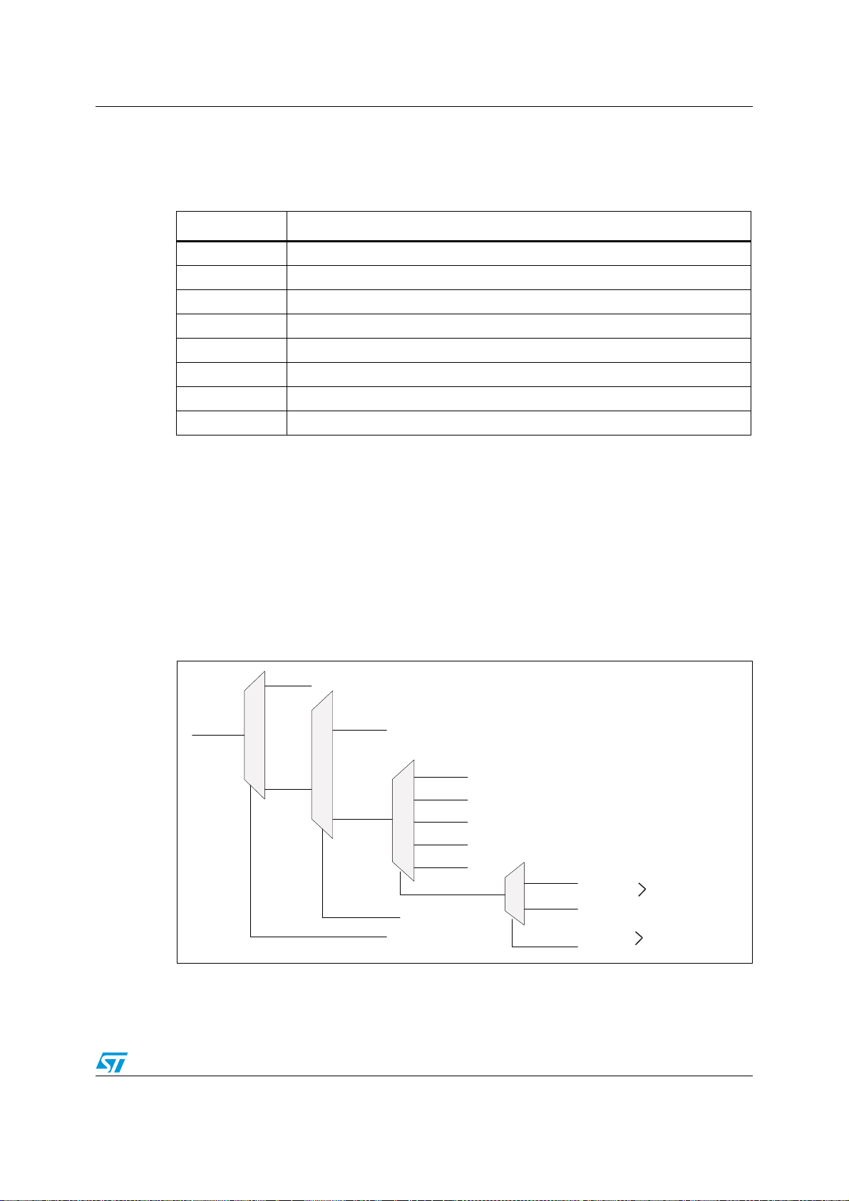
SPEAr320S Pin description
Extended mode
Mode 1: HMI automation
Mode 2: MII automation networking
Mode 3: Expanded automation
Mode 4: Printer
Mode 1/2/3/4 selector
Extended mode selector
Extended mode enable
RAS_Select_Reg
Alternate functions
GPIO_SELECT(0...3) registers
Control_Reg[2:0]
ExtControl_Reg[0]
3.4.4 Boot pins
The status of the boot pins is read at startup by the BootROM.
Table 14. Boot pins description
B3-B0 Boot device
0000 USB Device
0011 Serial NOR Flash (SMI interface)
0100 Parallel 8-bit NOR Flash (EMI interface)
0101 Parallel 16-bit NOR Flash (EMI interface)
0110 Parallel 8-bit NAND Flash (FSMC interface)
0111 Parallel 16-bit NAND Flash (FSMC interface)
1010 UART 0
Other Reserved
3.4.5 GPIOs
The PL_GPIO pins can be used as software-controlled general purpose I/Os if they are not
used by the interfaces of embedded IPs mapped on same pins.
3.4.6 Multiplexing scheme
To provide the best I/O multiplexing flexibility and the higher number of GPIOs for ARM
controlled input-output function, the following hierarchical multiplexing scheme has been
implemented.
Figure 3. Hierarchical multiplexing scheme
PL_GPIO
GPIOs
Note: Extended mode selector [2:0] registers are dedicated to each pin.
Doc ID 022508 Rev 1 39/97
Page 40
40/97 Doc ID 022508 Rev 1
Pin description SPEAr320S
Table 15. PL_GPIO multiplexing scheme
Configuration mode (SW defined) Alternate
PL_GPIO_# /
ball number
PL_GPIO_97/H16 CLD0 MII1_TXCLK EMI_A0 I2C2_SDA SSP1_MOSI GPIO_97
PL_GPIO_96/H15 CLD1 MII1_TXD0 EMI_A1 I2C2_SCL SSP1_CLK GPIO_96
PL_GPIO_95/H14 CLD2 MII1_TXD1 EMI_A2 UART3_TX SSP1_SS0 GPIO_95
PL_GPIO_94/H13 CLD3 MII1_TXD2 EMI_A3 UART3_RX SSP1_MISO GPIO_94
PL_GPIO_93/G17 CLD4 MII1_TXD3 EMI_A4 UART4_TX SSP2_MOSI GPIO_93
PL_GPIO_92/G16 CLD5 MII1_TXEN EMI_A5 UART4_ RX SSP2_CLK GPIO_92
PL_GPIO_91/G15 CLD6 MII1_TXER EMI_A6 UART5_T X SSP2_SS0 GPIO_91
PL_GPIO_90/G14 CLD7 MII1_RXCLK EMI_A7 UART5_R X SSP2_MISO GPIO_90
PL_GPIO_89/F17 CLD8 MII1_RXDV EMI_A8 UART 6_TX PWM0 GPIO_89
PL_GPIO_88/F16 CLD9 MII1_RXER EMI_A9 UART6_RX PWM1 GPIO_88
PL_GPIO_87/G13 CLD10 MII1_RXD0 EMI_A10 0 PWM2 GPIO_87
PL_GPIO_86/E17 CLD11 MII1_RXD1 EMI_A11 0 PWM3 GPIO_86
PL_GPIO_85/F15 CLD12 MII1_RXD2 EMI_A12 SPP_DATA0 UA RT1_CTS GPIO_85
PL_GPIO_84/D17 CLD13 MII1_RXD3 EMI_A13 SPP_DATA1 UART 1_DTR GPIO_84
PL_GPIO_83/E16 CLD14 MII1_COL EMI_A14 SPP_DATA2 UART1_RI GPIO_83
PL_GPIO_82/E15 CLD15 MII1_CRS EMI_A15 SPP_DATA3 UART1_DCD GPIO_82
PL_GPIO_81/C17 CLD16 MII1_MDIO EMI_A16 SPP_DATA4 UART 1_DS R GPIO_81
PL_GPIO_80/D16 CLD17 MII1_MDC EMI_A17 SPP_DATA5 UA RT1_RTS GPIO_80
PL_GPIO_79/F14 CLD18 0 EMI_A18 SPP_DATA6 UART_RS485_TX GPIO_79
PL_GPIO_78/D15 CLD19 0 EMI_A19 SPP_DATA7 UART_RS485_RX GPIO_78
PL_GPIO_77/B17 CLD20 0 EMI_A20 SPP_STRBn UART_RS485_OE GPIO_77
PL_GPIO_76/F13 CLD21 0 EMI_A21 SPP_ACKn I2C2_SDA GPIO_76
PL_GPIO_75/E14 CLD22 0 EMI_A22 SPP_BUSY I2C2_SCL GPIO_75
PL_GPIO_74/C16 CLD23 0 EMI_A23 SPP_PERROR UART3_T X GPIO_74
12 3 4Extended
function
(SW
defined)
Function in
Boot pins
GPIO
alternative
mode
Page 41
Table 15. PL_GPIO multiplexing scheme (continued)
SPEAr320S Pin description
Doc ID 022508 Rev 1 41/97
Configuration mode (SW defined) Alternate
PL_GPIO_# /
ball number
PL_GPIO_73/A17 CLAC 0 EMI_D8/ FSMC_D8 SPP_SELECT UART3_RX GPIO_73
PL_GPIO_72/B16 CLFP 0 EMI_D9/ FSMC_D9 SPP_AUTOFDn UA RT4_TX GPIO_72
PL_GPIO_71/D14 CLLP 0 EMI_D10/ FSMC_D10 SPP_FAULTn UART4_RX GPIO_71
PL_GPIO_70/C15 CLLE 0 EMI_D11/ FSMC_D11 SPP_INITn UART5 _TX GPIO_70
PL_GPIO_69/A16 CLPOWER 0 EMI_WAIT SPP_SELINn UART5_RX GPIO_69
PL_GPIO_68/B15 FSMC_D0 FSMC_D0 EMI_D0/ FSMC_D0 FSMC_D0 SSP1_MOSI GPIO_68
PL_GPIO_67/C14 FSMC_D1 FSMC_D1 EMI_D1/ FSMC_D1 FSMC_D1 SSP1_CLK GPIO_67
PL_GPIO_66/E13 FSMC_D2 FSMC_D2 EMI_D2/ FSMC_D2 FSMC_D2 SSP1_SS0 GPIO_66
PL_GPIO_65/B14 FSMC_D3 FSMC_D3 EMI_D3/ FSMC_D3 FSMC_D3 SSP1_MISO GPIO_65
PL_GPIO_64/D13 FSMC_D4 FSMC_D4 EMI_D4/ FSMC_D4 FSMC_D4 SSP2_MOSI GPIO_64
PL_GPIO_63/C13 FSMC_D5 FSMC_D5 EMI_D5/ FSMC_D5 FSMC_D5 SSP2_CLK GPIO_63
PL_GPIO_62/A15 FSMC_D6 FSMC_D6 EMI_D6/ FSMC_D6 FSMC_D6 SSP2_SS0 H7 GPIO_62
PL_GPIO_61/E12 FSMC_D7 FSMC_D7 EMI_D7/ FSMC_D7 FSMC_D7 SSP2_MISO H6 GPIO_61
PL_GPIO_60/A14 FSMC_ADDR_LE FSMC_ADDR_LE FSMC_ADDR_LE FSMC_ADDR_LE PWM0 H5 GPIO_60
PL_GPIO_59/B13 FSMC_WE FSMC_WE EMI_WE/ FSMC_WE FSMC_WE PWM1 H4 GPIO_59
PL_GPIO_58/D12 FSMC_RE FSMC_RE EMI_OE/ FSMC_RE FSMC_RE PWM2 H3 GPIO_58
PL_GPIO_57/E11 FSMC_CMD_ LE FSMC_CMD_ LE FSMC_CMD_LE FSMC_CMD_LE PWM3 H2 GPIO_57
PL_GPIO_56/C12 FSMC_RDY /BSY FSMC_RDY/ BSY FSMC_RDY/BSY FSMC_RDY/ BSY H1 GPIO_56
PL_GPIO_55/A13 FSMC_CS0 FSMC_CS0 EMI_CE0/ FSMC_CS0 FSMC_CS0 H0 GPIO_55
PL_GPIO_54/E10 FSMC_CS1 FSMC_CS1 EMI_CE1/ FSMC_CS1 FSMC_CS1 B3 GPIO_54
PL_GPIO_53/D11 FSMC_CS2 FSMC_CS2 EMI_CE2/ FSMC_CS2 FSMC_CS2 UART3_TX B2 GPIO_53
PL_GPIO_52/B12 FSMC_CS3 FSMC_CS3 EMI_CE_3/ FSMC_CS3 FSMC_CS3 UART3_R X B1 GPIO_52
PL_GPIO_51/D10 SD_CD SD_CD EMI_BYTEN0 SD_CD SSP1_MOSI B0 GPIO_51
PL_GPIO_50/A12 SD_DAT7 SD_DAT7 EMI_BYTEN1 SD_DAT7 SSP1_CLK TMR_CPTR4 GPIO_50
PL_GPIO_49/C11 SD_DAT6 SD_DAT6 EMI_D12/ FSMC_D12 SD_DAT6 SSP1_SS0 TMR_CPTR3 GPIO_49
PL_GPIO_48/B11 SD_DAT5 SD_DAT5 EMI_D13/ FSMC_D13 SD_DAT5 SSP1_MISO TMR_CPTR2 GPIO_48
12 3 4Extended
function
(SW
defined)
Function in
Boot pins
GPIO
alternative
mode
Page 42
42/97 Doc ID 022508 Rev 1
Table 15. PL_GPIO multiplexing scheme (continued)
Pin description SPEAr320S
Configuration mode (SW defined) Alternate
PL_GPIO_# /
ball number
PL_GPIO_47/C10 SD_DAT4 SD_DAT4 EMI_D14/ FSMC_D14 SD_DAT4 SSP2_MOSI TMR_CPTR1 GPIO_47
PL_GPIO_46/A11 SD_DAT3 SD_DAT3 EMI_D15/ FSMC_D15 SD_DAT3 SSP2_CLK TMR_CLK4 GPIO_46
PL_GPIO_45/B10 SD_DAT2 SD_DAT2 UART1_DCD SD_DAT2 SSP2_SS0 TMR_CLK3 GPIO_45
PL_GPIO_44/A10 SD_DAT1 SD_DAT1 UART 1_DSR SD_DAT1 SSP2_MISO TMR_CLK2 GPIO_44
PL_GPIO_43/E9 SD_DAT0 SD_DAT0 UART1_RTS SD_DAT0 PWM0 TMR_CLK1 GPIO_43
PL_GPIO_42/D9 I2S_RX I2S_RX UART3_TX 0 PWM1 UART0_DTR GPIO_42
PL_GPIO_41/C9 I2S_TX I2S_TX UART3_RX 0 PWM2 UART 0_R I GPIO_41
PL_GPIO_40/B9 I2S_LR I2S_LR UART4_TX 0 PWM3 UART0 _DS R GPIO_40
PL_GPIO_39/A9 I2S_CLK I2S_CLK UART4_ RX 0 SSP1_MOSI UART0_DCD GPIO_39
PL_GPIO_38/A8 PWM0 PWM0 UART5_TX 0 SSP1_CLK UART0_CTS GPIO_38
PL_GPIO_37/B8 PWM1 PWM1 UART5_RX 0 SSP1_SS0 UART0_RTS GPIO_37
PL_GPIO_36/C8 TOUCHSCREEN X 0 UART1_CTS UART1_CTS SSP1_MISO SSP0_CS4 GPIO_36
PL_GPIO_35/D8
PL_GPIO_34/E8 SD_LED / PWM2 SD_LED / PWM2 UART1_RI UART1_R I SSP2_CLK SSP0_CS2 GPIO_34
PL_GPIO_33/E7 CAN0_TX CAN0_TX CAN0_TX UART1_DCD SSP2_SS0 basGPIO5 GPIO_33
PL_GPIO_32/D7 CAN0_RX CAN0_RX CAN0_RX UART1_DSR SSP2_MISO basGPIO4 GPIO_32
PL_GPIO_31/C7 CAN1_TX CAN1_TX CAN1_TX UART1_RTS PWM0 basGPIO3 GPIO_31
PL_GPIO_30/B7 CAN1_RX CAN1_RX CAN1_RX 0 PWM1 basGPIO2 GPIO_30
PL_GPIO_29/A7 UART1_TX UART1_TX UART1_TX UART1_T X PWM2 basGPIO1 GPIO_29
PL_GPIO_28/A6 UART1_RX UART 1_R X UART1_RX UART1_RX PWM3 basGPIO0 GPIO_28
PL_GPIO_27/B6 Reserved 0 Reserved Reserved RMII0_TXD0 MII0_TXCLK GPIO_27
PL_GPIO_26/A5 Reserved 0 Reserved Reserved RMII0_RXD0 MII0_TXD0 GPIO_26
PL_GPIO_25/C6 Reserved 00ReservedRMII1_TXD0 MII0_TXD1 GPIO_25
PL_GPIO_24/B5 Reserved 00ReservedRMII1_RXD0 MII0_TXD2 GPIO_24
PL_GPIO_23/A4 Reserved 0 Reserved Reserved RMII1_TX_EN MII0_TXD3 GPIO_23
12 3 4Extended
audio_over_sam
p_clk
audio_over_sam
p_clk
UART1_DTR UART1_DTR SSP2_MOSI SSP0_CS3 GPIO_35
function
(SW
defined)
Function in
Boot pins
GPIO
alternative
mode
Page 43
Table 15. PL_GPIO multiplexing scheme (continued)
SPEAr320S Pin description
Doc ID 022508 Rev 1 43/97
Configuration mode (SW defined) Alternate
PL_GPIO_# /
ball number
PL_GPIO_22/D6 Reserved 0 Reserved Reserved RMII_REF_CLK MII0_TXEN GPIO_22
PL_GPIO_21/C5 Reserved 0 Reserved Reserved RMII1_TXD1 MII0_TXER GPIO_21
PL_GPIO_20/B4 SSP1_MOSI I2C2_SDA 0 SSP1_MOSI RMII1_RXD1 MII0_RXCLK GPIO_20
PL_GPIO_19/A3 SSP1_CLK I2C2_SCL 0 SSP1_CLK RMII1_CRS_DV MII0_RXDV GPIO_19
PL_GPIO_18/D5 SSP1_SS0 0 0 SSP1_SS0 RMII1_RX_ER MII0_RXER GPIO_18
PL_GPIO_17/C4 SSP1_MISO 0 0 SSP1_MISO RMII0_TXD1 MII0_RXD0 GPIO_17
PL_GPIO_16/E6 SSP2_MOSI UART3_TX 0 0 RMII0_TX_EN MII0_RXD1 GPIO_16
PL_GPIO_15/B3 SSP2_CLK UART3_RX PWM0 PWM0 RMII0_RXD1 MII0_RXD2 GPIO_15
PL_GPIO_14/A2 SSP2_SS0 UART4_TX PWM1 PWM1 RMII0_CRS_DV MII0_RXD3 GPIO_14
PL_GPIO_13/A1 SSP2_MISO UART4_RX PWM2 PWM2 RMII0_RX_ER MII0_COL GPIO_13
PL_GPIO_12/D4 PWM3 0 PWM3 PWM3 SD_CD MII0_CRS GPIO_12
PL_GPIO_11/E5 Reserved 0 Reserved Reserved RMII_MDC MII0_MDC GPIO_11
PL_GPIO_10/C3 Reserved 0 Reserved Reserved RMII_MDIO MII0_MDIO GPIO_10
PL_GPIO_9/B2 0 UART3_TX PWM0 0 I2C1_SDA SSP0_MOSI GPIO_9
PL_GPIO_8/C2 0 UA RT3_ RX PWM1 0 I2C1_SCL SSP0_CLK GPIO_8
PL_GPIO_7/D3 0 UART4_TX PWM2 0 UART1 _CT S SSP0_SS0 GPIO_7
PL_GPIO_6/B1 0 UART4_RX PWM3 0 UART1_DTR SSP0_MISO GPIO_6
PL_GPIO_5/D2 0 UART5_TX 0 0 UART1_RI I2C0_SDA GPIO_5
PL_GPIO_4/C1 0 UA RT5_ RX 0 0 UART1_DCD I2C0_SCL GPIO_4
PL_GPIO_3/D1 I2C2_SDA UART6_TX 0 0 UART1_DSR UART0_RX GPIO_3
PL_GPIO_2/E4 I2C2_SCL UA RT6_ RX 0 0 UART1_RTS UART0_TX GPIO_2
PL_GPIO_1/E3 UART2_TX UART2_TX UART2_TX UART2_TX I2C2_SDA IrDA_RX GPIO_1
PL_GPIO_0/F3 UART2 _RX UART 2_RX UA RT2_RX UART2_RX I2C2_SCL IrDA_TX GPIO_0
PL_CLK1/K17 CLCP 0 I2C1_SDA SD_LED UA RT3_ TX PL_CLK1 GPIO_98
PL_CLK2/J17 SD_CLK SD_CLK I2C1_SCL SD_CLK UART3 _RX PL_CLK2 GPIO_99
12 3 4Extended
function
(SW
defined)
Function in
Boot pins
GPIO
alternative
mode
Page 44
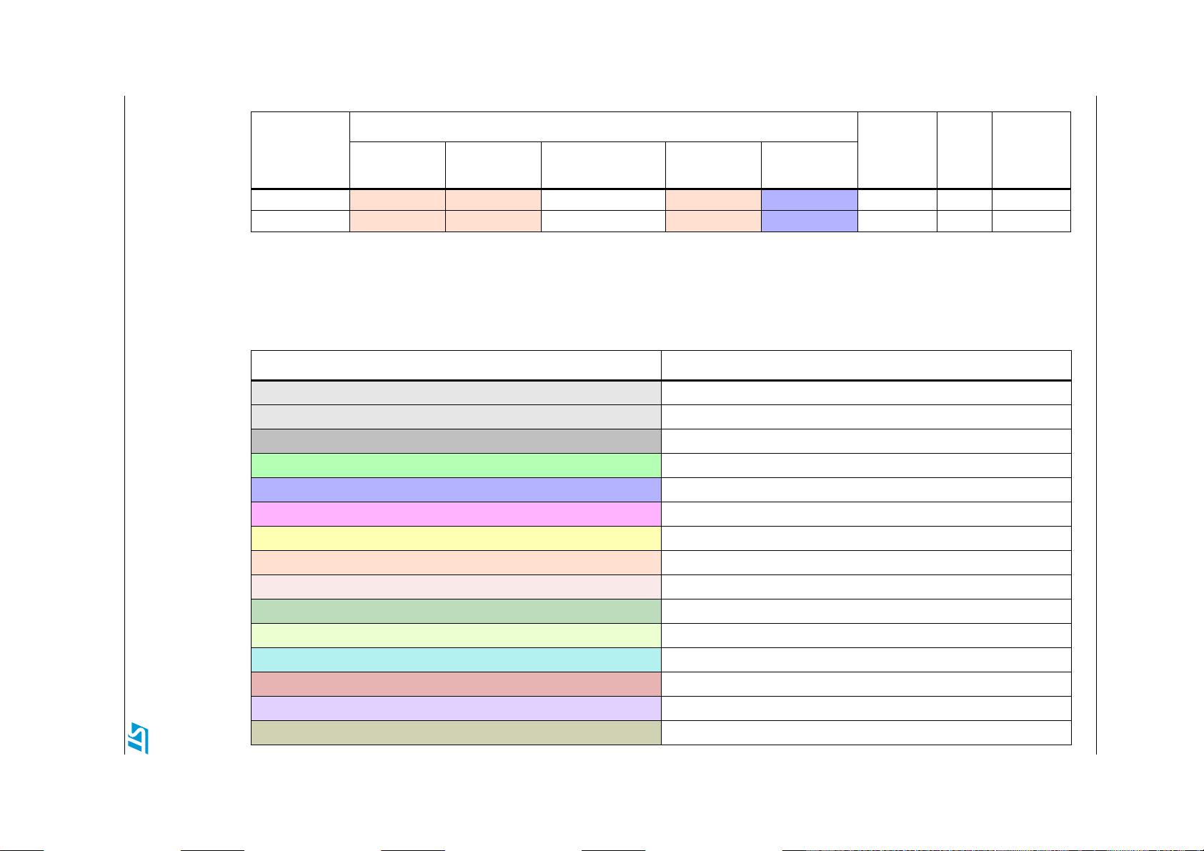
44/97 Doc ID 022508 Rev 1
Table 15. PL_GPIO multiplexing scheme (continued)
Pin description SPEAr320S
Configuration mode (SW defined) Alternate
PL_GPIO_# /
ball number
PL_CLK3/J16 SD_WP SD_WP 0 SD_WP UART4_T X PL_CLK3 GPIO_100
PL_CLK4/H17 SD_CMD SD_CMD 0 SD_CMD UART4_RX PL_CLK4 GPIO_101
12 3 4Extended
function
(SW
defined)
Function in
Boot pins
GPIO
alternative
mode
Note: 1 Ta b l e 1 5 cells filled with ‘0’ or ‘1’ are unused and unless otherwise configured as Alternate function or GPIO, the corresponding pin
is held at low or high level respectively by the internal logic.
2Pins shared by EMI and FSMC: Depending on the AHB address to be accessed the pins are used for EMI or FSMC transfers.
Table 16. Table shading
Shading Pin group
FSMC FSMC pins: NAND Flash
EMI EMI pins
CLCD Color LCD controller pins
Touchscreen Touchscreen pins
UART UART pins
CAN CAN pins
Ethernet MAC MII/RMII Ethernet MAC pins
SD/SDIO/MMC SD card controller pins
PWM generators Pulse-width modulator timer module pins
GPT Timer pins
IrDa IrDa pins
SSP SSP pins
I2C I2C pins
Standard Parallel port Standard parallel port pins
I2S I2S pins
Page 45
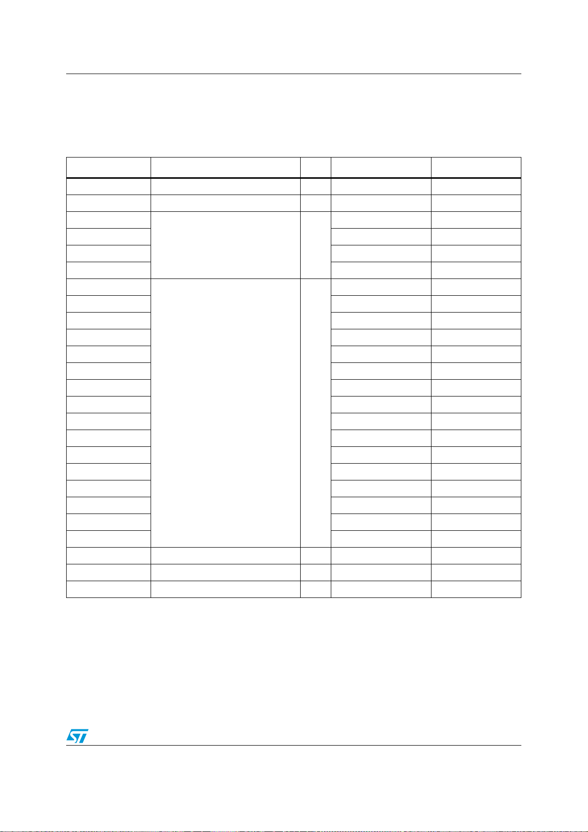
SPEAr320S Pin description
3.4.7 Multiplexed signals description
This section provides a description of the multiplexed signals present in SPEAr320S device,
grouped by IP.
Table 17. FSMC signals description
Signal name Description Dir. PL_GPIO_# /Ball Configuration mode
FSMC_ADDR_LE Address latch enable (active high) O PL_GPIO_60/A14 1, 2, 3, 4
FSMC_CMD_ LE Command latch enable (active high) O PL_GPIO_57/E11 1, 2, 3, 4
FSMC_CS0
FSMC_CS1 PL_GPIO_54/E10 1, 2, 3, 4
FSMC_CS2 PL_GPIO_53/D11 1, 2, 3, 4
FSMC_CS3 PL_GPIO_52/B12 1, 2, 3, 4
FSMC_D0
FSMC_D1 PL_GPIO_67/C14 1, 2, 3, 4
FSMC_D2 PL_GPIO_66/E13 1, 2, 3, 4
FSMC_D3 PL_GPIO_65/B14 1, 2, 3, 4
PL_GPIO_55/A13 1, 2, 3, 4
Chip enable (active low) O
PL_GPIO_68/B15 1, 2, 3, 4
FSMC_D4 PL_GPIO_64/D13 1, 2, 3, 4
FSMC_D5 PL_GPIO_63/C13 1, 2, 3, 4
FSMC_D6 PL_GPIO_62/A15 1, 2, 3, 4
FSMC_D7 PL_GPIO_61/E12 1, 2, 3, 4
Data lines IO
FSMC_D8 PL_GPIO_73/A17 3
FSMC_D9 PL_GPIO_72/B16 3
FSMC_D10 PL_GPIO_71/D14 3
FSMC_D11 PL_GPIO_70/C15 3
FSMC_D12 PL_GPIO_49/C11 3
FSMC_D13 PL_GPIO_48/B11 3
FSMC_D14 PL_GPIO_47/C10 3
FSMC_D15 PL_GPIO_46/A11 4
FSMC_RDY/BSY Wait signal (active low) I PL_GPIO_56/C12 1, 2, 3, 4
FSMC_RE Read enable (active low) O PL_GPIO_58/D12 1, 2, 3, 4
FSMC_WE Write enable (active low) O PL_GPIO_59/B13 1, 2, 3, 4
Doc ID 022508 Rev 1 45/97
Page 46
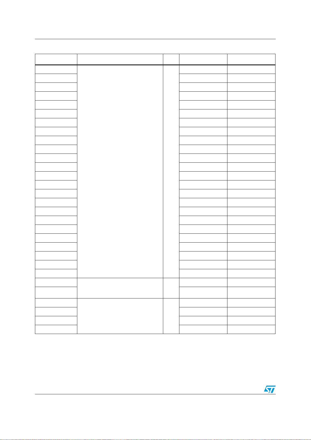
Pin description SPEAr320S
Table 18. EMI signals description
Signal name Description Dir. PL_GPIO_# /Ball Configuration mode
EMI_A0
EMI_A1 PL_GPIO_96/H15 3
EMI_A2 PL_GPIO_95/H14 3
EMI_A3 PL_GPIO_94/H13 3
EMI_A4 PL_GPIO_93/G17 3
EMI_A5 PL_GPIO_92/G16 3
EMI_A6 PL_GPIO_91/G15 3
EMI_A7 PL_GPIO_90/G14 3
EMI_A8 PL_GPIO_89/F17 3
EMI_A9 PL_GPIO_88/F16 3
EMI_A10 PL_GPIO_87/G13 3
EMI_A11 PL_GPIO_86/E17 3
Address bus O
EMI_A12 PL_GPIO_85/F15 3
EMI_A13 PL_GPIO_84/D17 3
EMI_A14 PL_GPIO_83/E16 3
EMI_A15 PL_GPIO_82/E15 3
EMI_A16 PL_GPIO_81/C17 3
EMI_A17 PL_GPIO_80/D16 3
PL_GPIO_97/H16 3
EMI_A18 PL_GPIO_79/F14 3
EMI_A19 PL_GPIO_78/D15 3
EMI_A20 PL_GPIO_77/B17 3
EMI_A21 PL_GPIO_76/F13 3
EMI_A22 PL_GPIO_75/E14 3
EMI_A23 PL_GPIO_74/C16 3
EMI_BYTEN0 Byte_enables are provided to validate
EMI_BYTEN1 PL_GPIO_50/A12 3
EMI_CE0
EMI_CE1 PL_GPIO_54/E10 3
EMI_CE2 PL_GPIO_53/D11 3
EMI_CE3 PL_GPIO_52/B12 3
the data present on the bus when high
data is valid.
EMI Chip selects, derived from internal
address decoding
(kept disabled during NAND_Flash
cycles)
IO
O
PL_GPIO_51/D10 3
PL_GPIO_55/A13 3
46/97 Doc ID 022508 Rev 1
Page 47
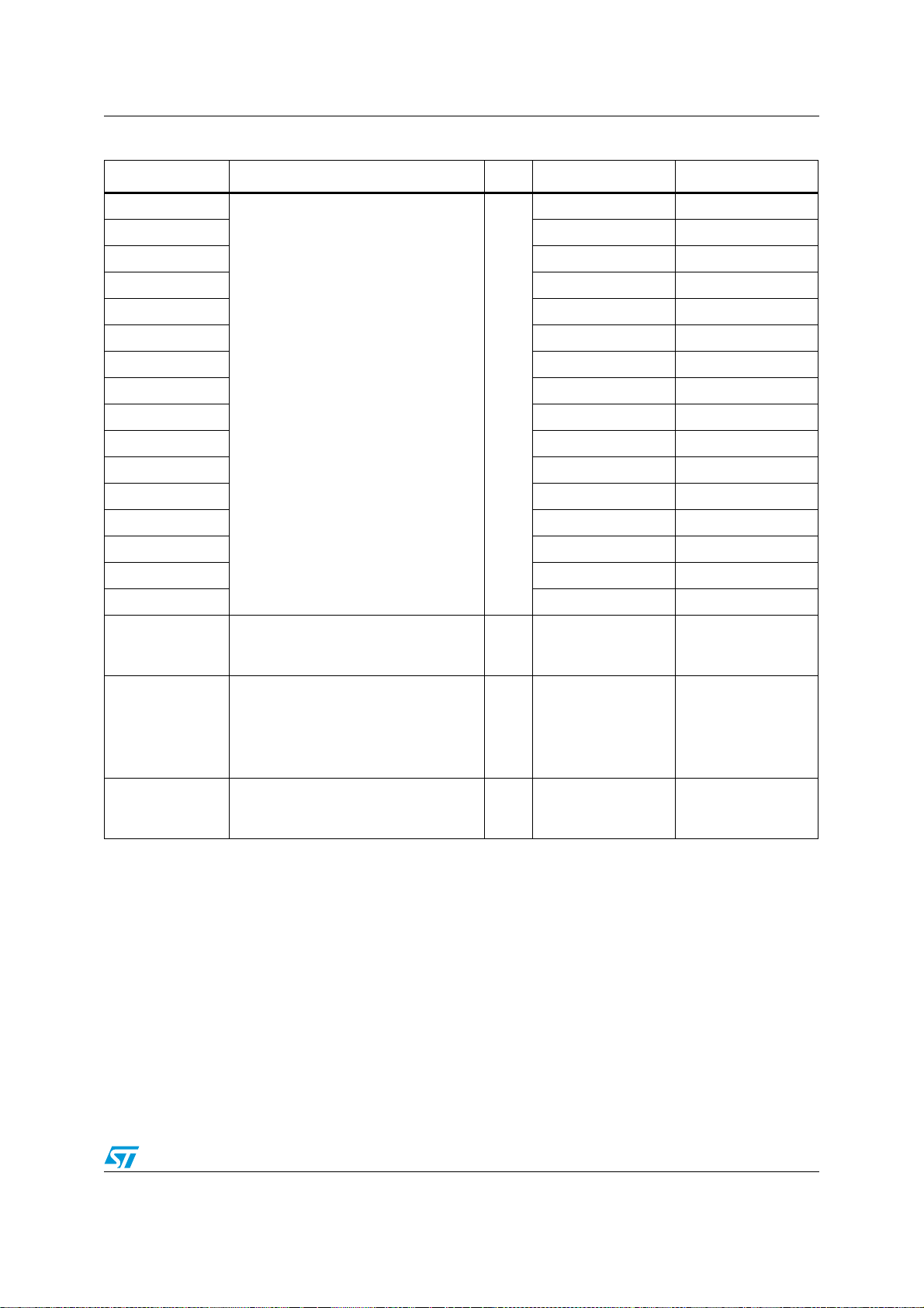
SPEAr320S Pin description
Table 18. EMI signals description (continued)
Signal name Description Dir. PL_GPIO_# /Ball Configuration mode
EMI_D0
EMI_D1 PL_GPIO_67/C14 3
EMI_D2 PL_GPIO_66/E13 3
EMI_D3 PL_GPIO_65/B14 3
EMI_D4 PL_GPIO_64/D13 3
EMI_D5 PL_GPIO_63/C13 3
EMI_D6 PL_GPIO_62/A15 3
EMI_D7 PL_GPIO_61/E12 3
EMI_D8 PL_GPIO_73/A17 3
EMI_D9 PL_GPIO_72/B16 3
EMI_D10 PL_GPIO_71/D14 3
EMI_D11 PL_GPIO_70/C15 3
EMI_D12 PL_GPIO_49/C11 3
EMI_D13 PL_GPIO_48/B11 3
EMI_D14 PL_GPIO_47/C10 3
EMI_D15 PL_GPIO_46/A11 3
EMI_OE
EMI_WAIT
EMI_WE
Data bus O
Data output enable for read cycles,
target device must open its data bus
with this signal.
Transfer acknowledge signal, used by
the cycle target to slow down the cycle
(must be pulled up on the bus for
targets that do not need it).
Note: This is an optional signal.
Write strobe, data are ready on
EMI_ADB before its falling edge and
after the rising edge.
O PL_GPIO_58/D12 3
I PL_GPIO_69/A16 3
O PL_GPIO_59/B13 3
PL_GPIO_68/B15 3
Doc ID 022508 Rev 1 47/97
Page 48
Pin description SPEAr320S
Table 19. CLCD signals description
Signal name Description Dir. PL_GPIO_# /Ball Configuration mode
CLAC
STN AC bias drive or TFT data enable
output
O PL_GPIO_73/A17 1
CLCP LCD panel clock O PL_CLK1/K17 1
CLD0
PL_GPIO_97/H16
CLD1 PL_GPIO_96/H15
CLD2 PL_GPIO_95/H14
CLD3 PL_GPIO_94/H13
CLD4 PL_GPIO_93/G17
CLD5 PL_GPIO_92/G16
CLD6 PL_GPIO_91/G15
CLD7 PL_GPIO_90/G14
CLD8 PL_GPIO_89/F17
CLD9 PL_GPIO_88/F16
CLD10 PL_GPIO_87/G13
CLD11 PL_GPIO_86/E17
LCD panel data O
1
CLD12 PL_GPIO_85/F15
CLD13 PL_GPIO_84/D17
CLD14 PL_GPIO_83/E16
CLD15 PL_GPIO_82/E15
CLD16 PL_GPIO_81/C17
CLD17 PL_GPIO_80/D16
CLD18 PL_GPIO_79/F14
CLD19 PL_GPIO_78/D15
CLD20 PL_GPIO_77/B17
CLD21 PL_GPIO_76/F13
CLD22 PL_GPIO_75/E14
CLD23 PL_GPIO_74/C16
CLFP
Frame pulse (STN)/ vertical
synchronization pulse (TFT)
O PL_GPIO_72/B16 1
CLLE Line end signal O PL_GPIO_70/C15 1
CLLP
Line synchronization pulse (STN)/
horizontal synchronization pulse (TFT)
O PL_GPIO_71/D14 1
CLPOWER LCD panel power enable O PL_GPIO_69/A16 1
48/97 Doc ID 022508 Rev 1
Page 49
SPEAr320S Pin description
Table 20. Touchscreen signal description
Signal name Description Dir. PL_GPIO_# /Ball
Configuration
mode
TOUCHSCREEN X Touchscreen select signal O PL_GPIO_36/C8 1
Table 21. UART signals description
Signal name Description Dir. PL_GPIO_# /Ball
Configuration
mode
UART0
UART0_CTS UART0 clear to send modem status input I PL_GPIO_38/A8 Alternate function
UART0_DCD
UART0 data carrier detect modem status
input
I PL_GPIO_39/A9 Alternate function
UART0_DSR UART0 data set ready modem status input I PL_GPIO_40/B9 Alternate function
UART0_DTR
UART0 data terminal ready modem status
output
O PL_GPIO_42/D9 Alternate function
UART0_RI UART0 ring indicator modem status input I PL_GPIO_41/C9 Alternate function
UART0_RTS
UART0 request to send modem status
output
O PL_GPIO_37/B8 Alternate function
UART0_RX UART0 received serial data input I PL_GPIO_3/D1 Alternate function
UART0_TX UART0 transmitted serial data output O PL_GPIO_2/E4 Alternate function
UART1
PL_GPIO_36/C8 3, 4
UART1_CTS UART1 clear to send modem status input I
PL_GPIO_85/F15
Extended mode
PL_GPIO_7/D3
PL_GPIO_45/B10 3
UART1_DCD
UART1 data carrier detect modem status
input
PL_GPIO_33/E7 4
I
PL_GPIO_4/C1
Extended mode
PL_GPIO_82/E15
PL_GPIO_44/A10 3
PL_GPIO_32/D7 4
UART1_DSR UART1 data set ready modem status input I
PL_GPIO_3/D1
Extended mode
PL_GPIO_81/C17
PL_GPIO_35/D8 3, 4
UART1_DTR
UART1 data terminal ready modem status
output
O
PL_GPIO_84/D17
Extended mode
PL_GPIO_6/B1
PL_GPIO_34/E8 3, 4
UART1_RI UART1 ring indicator modem status input I
PL_GPIO_83/E16
Extended mode
PL_GPIO_5/D2
Doc ID 022508 Rev 1 49/97
Page 50
Pin description SPEAr320S
Table 21. UART signals description (continued)
Signal name Description Dir. PL_GPIO_# /Ball
PL_GPIO_43/E9 3
UART1_RTS
UART1_RX UART1 received serial data input I PL_GPIO_28/A6 1, 2, 3, 4
UART1_TX UART1 transmitted serial data output O PL_GPIO_29/A7 1, 2, 3, 4
UART2
UART2_RX UART2 received serial data input I PL_GPIO_0/F3 1, 2, 3, 4
UART2_TX UART2 transmitted serial data output O PL_GPIO_1/E3 1, 2, 3, 4
UART3
UART3_RX UART3 received serial data input I
UART1 request to send modem status
output
PL_GPIO_31/C7 4
O
PL_GPIO_80/D16
PL_GPIO_2/E4
PL_GPIO_15/B3
PL_GPIO_8/C2
PL_GPIO_41/C9 3
PL_GPIO_94/H13 4
PL_GPIO_73/A17
PL_CLK2/J17
Configuration
Extended mode
2
Extended modePL_GPIO_52/B12
mode
UART3_TX UART3 transmitted serial data output O
UART4
UART4_RX UART4 received serial data input
PL_GPIO_16/E6
PL_GPIO_9/B2
PL_GPIO_42/D9 3
PL_GPIO_95/H14 4
PL_GPIO_74/C16
PL_CLK1/K17
PL_GPIO_13/A1
PL_GPIO_6/B1
I
PL_GPIO_39/A9 3
PL_GPIO_92/G16 4
PL_GPIO_71/D14
I
PL_CLK4/H17
2
Extended modePL_GPIO_53/D11
2
Extended mode
50/97 Doc ID 022508 Rev 1
Page 51
SPEAr320S Pin description
Table 21. UART signals description (continued)
Signal name Description Dir. PL_GPIO_# /Ball
PL_GPIO_14/A2
PL_GPIO_7/D3
PL_GPIO_40/B9 3
UART4_TX UART4 transmitted serial data output O
PL_GPIO_93/G17 4
PL_GPIO_72/B16
PL_CLK3/J16
UART5
PL_GPIO_4/C1 2
PL_GPIO_37/B8 3
UART5_RX UART5 received serial data input I
PL_GPIO_90/G14 4
PL_GPIO_69/A16 Extended mode
PL_GPIO_5/D2 2
PL_GPIO_38/A8 3
UART5_TX UART5 transmitted serial data output O
PL_GPIO_91/G15 4
PL_GPIO_70/C15 Extended mode
UART6
PL_GPIO_2/E4 2
UART6_RX UART6 received serial data input I
PL_GPIO_88/F16 4
PL_GPIO_3/D1 2
UART6_TX UART6 transmitted serial data output O
PL_GPIO_89/F17 4
Configuration
mode
2
Extended mode
UART/RS485
UART_RS485_TX UART/RS485 transmitted serial data output O PL_GPIO_79/F14 Extended mode
UART_RS485_RX UART/RS485 received serial data output I
UART_RS485_OE UART/RS485 data output enable O
Table 22. CAN signals description
Signal name Description Dir. PL_GPIO_# /Ball
PL_GPIO_78/D15 Extended mode
PL_GPIO_77/B17 Extended mode
Configuration
mode
CAN0
CAN0_RX CAN0 receiver data input I PL_GPIO_32/D7 1, 2, 3
CAN0_TX CAN0 transmitter data output O PL_GPIO_33/E7 1, 2, 3
CAN1
CAN1_RX CAN1 receiver data input I PL_GPIO_30/B7 1, 2, 3
CAN1_TX CAN1 transmitter data output O PL_GPIO_31/C7 1, 2, 3
Doc ID 022508 Rev 1 51/97
Page 52
Pin description SPEAr320S
Table 23. MMC-SD/SDIO controller signals description
Signal name Description Dir. PL_GPIO_# /Ball Configuration mode
SD_CD
Card detection for single slot
(active low)
I
PL_GPIO_51/D10 1, 2, 4
PL_GPIO_12/D4 Extended mode
SD_CLK Clock to external card O PL_CLK2/J17 1, 2, 4
SD_CMD Command line IO PL_CLK4/H17 1, 2, 4
SD_DAT0
PL_GPIO_43/E9 1, 2, 4
SD_DAT1 PL_GPIO_44/A10 1, 2, 4
SD_DAT2 PL_GPIO_45/B10 1, 2, 4
SD_DAT3 PL_GPIO_46/A11 1, 2, 4
Data line IO
SD_DAT4 PL_GPIO_47/C10 1, 2, 4
SD_DAT5 PL_GPIO_48/B11 1, 2, 4
SD_DAT6 PL_GPIO_49/C11 1, 2, 4
SD_DAT7 PL_GPIO_50/A12 1, 2, 4
SD_LED
Cautions the user not to remove the
card while the SD card is being
accessed.
O
PL_GPIO_34/E8 1, 2
PL_CLK1/K17 4
SD_WP SD card write protect (active low) I PL_CLK3/J16 1, 2, 4
Table 24. PWM signals description
Signal name Description Dir. PL_GPIO_# /Ball Configuration mode
PL_GPIO_38/A8 1, 2
PL_GPIO_15/B3 3, 4
PL_GPIO_9/B2 3
PWM0 PWM0 output channel O
PL_GPIO_89/F17
PL_GPIO_60/A14
Extended mode
PL_GPIO_43/E9
PL_GPIO_31/C7
PL_GPIO_37/B8 1, 2
PL_GPIO_14/A2 3, 4
PL_GPIO_8/C2 3
PWM1 PWM1 output channel O
PL_GPIO_88/F16
PL_GPIO_59/B13
Extended mode
PL_GPIO_42/D9
PL_GPIO_30/B7
52/97 Doc ID 022508 Rev 1
Page 53
SPEAr320S Pin description
Table 24. PWM signals description (continued)
Signal name Description Dir. PL_GPIO_# /Ball Configuration mode
PL_GPIO_34/E8 1, 2
PL_GPIO_13/A1 3, 4
PL_GPIO_7/D3 3
PWM2 PWM2 output channel O
PL_GPIO_87/G13
PL_GPIO_58/D12
Extended mode
PL_GPIO_41/C9
PL_GPIO_29/A7
PL_GPIO_12/D4 1, 3, 4
PL_GPIO_6/B1 3
PL_GPIO_86/E17
PWM3 PWM3 output channel O
PL_GPIO_57/E11
Extended mode
PL_GPIO_40/B9
PL_GPIO_28/A6
Table 25. GPT signals description
Signal name Description Dir. PL_GPIO_# /Ball Configuration mode
TMR_CLK1
TMR_CLK2 PL_GPIO_44/A10 Alternate function
TMR_CLK3 PL_GPIO_45/B10 Alternate function
This clock toggles each time the
timer interrupt goes active.
O
PL_GPIO_43/E9 Alternate function
TMR_CLK4 PL_GPIO_46/A11 Alternate function
TMR_CPTR1
PL_GPIO_47/C10 Alternate function
TMR_CPTR2 PL_GPIO_48/B11 Alternate function
TMR_CPTR3 PL_GPIO_49/C11 Alternate function
Asynchronous signal provided for
the measurement of timing signals
I
TMR_CPTR4 PL_GPIO_50/A12 Alternate function
Table 26. IrDA signals description
Signal name Description Dir. PL_GPIO_# /Ball Configuration mode
IrDA_RX IrDA receiver data input I PL_GPIO_1/E3 Alternate function
IrDA_TX IrDA transmitter data output O PL_GPIO_0/F3 Alternate function
Doc ID 022508 Rev 1 53/97
Page 54
Pin description SPEAr320S
Table 27. SSP signals description
Signal name Description Dir. PL_GPIO_# /Ball Configuration mode
SSP0
SSP0_CS2
SSP0_CS3
SSP0_CS4
SSP0_CLK
Slave select (used only in master
mode)
Slave select (used only in master
mode)
Slave select (used only in master
mode)
SSP clock. It is used as output in
master mode as input in slave mode.
O PL_GPIO_34/E8 Alternate function
O PL_GPIO_35/D8 Alternate function
O PL_GPIO_36/C8 Alternate function
IO PL_GPIO_8/C2 Alternate function
SSP0_MISO Master input slave output IO PL_GPIO_6/B1 Alternate function
SSP0_MOSI Master output slave input IO PL_GPIO_9/B2 Alternate function
SSP0_SS0
SSP frame output (master mode),
input (slave mode)
IO PL_GPIO_7/D3 Alternate function
SSP1
PL_GPIO_19/A3 1, 4
PL_GPIO_96/H15
SSP1_CLK
SSP clock. It is used as output in
master mode as input in slave mode.
IO
PL_GPIO_67/C14
Extended mode
PL_GPIO_50/A12
PL_GPIO_38/A8
PL_GPIO_17/C4 1, 4
SSP1_MISO Master input slave output IO
SSP1_MOSI Master output slave input IO
SSP1_SS0
SSP frame output (master mode),
input (slave mode)
IO
SSP2
PL_GPIO_94/H13
PL_GPIO_65/B14
Extended mode
PL_GPIO_48/B11
PL_GPIO_36/C8
PL_GPIO_20/B4 1, 4
PL_GPIO_97/H16
PL_GPIO_68/B15
Extended mode
PL_GPIO_51/D10
PL_GPIO_39/A9
PL_GPIO_18/D5 1, 4
PL_GPIO_95/H14
PL_GPIO_66/E13
Extended mode
PL_GPIO_49/C11
PL_GPIO_37/B8
54/97 Doc ID 022508 Rev 1
Page 55
SPEAr320S Pin description
Table 27. SSP signals description (continued)
Signal name Description Dir. PL_GPIO_# /Ball Configuration mode
PL_GPIO_15/B3 1
PL_GPIO_92/G16
SSP2_CLK
SSP clock. It is used as output in
master mode as input in slave mode.
IO
PL_GPIO_63/C13
Extended mode
PL_GPIO_46/A11
PL_GPIO_34/E8
PL_GPIO_13/A1 1
PL_GPIO_90/G14
SSP2_MISO Master input slave output IO
SSP2_MOSI Master output slave input IO
SSP2_SS0
SSP frame output (master mode),
input (slave mode)
IO
PL_GPIO_61/E12
PL_GPIO_44/A10
PL_GPIO_32/D7
PL_GPIO_16/E6 1
PL_GPIO_47/C10
PL_GPIO_35/D8
PL_GPIO_16/E6
PL_GPIO_93/G17
PL_GPIO_64/D13
PL_GPIO_14/A2 1
PL_GPIO_91/G15
PL_GPIO_62/A15
PL_GPIO_45/B10
PL_GPIO_33/E7
Extended mode
Extended mode
Extended mode
Doc ID 022508 Rev 1 55/97
Page 56
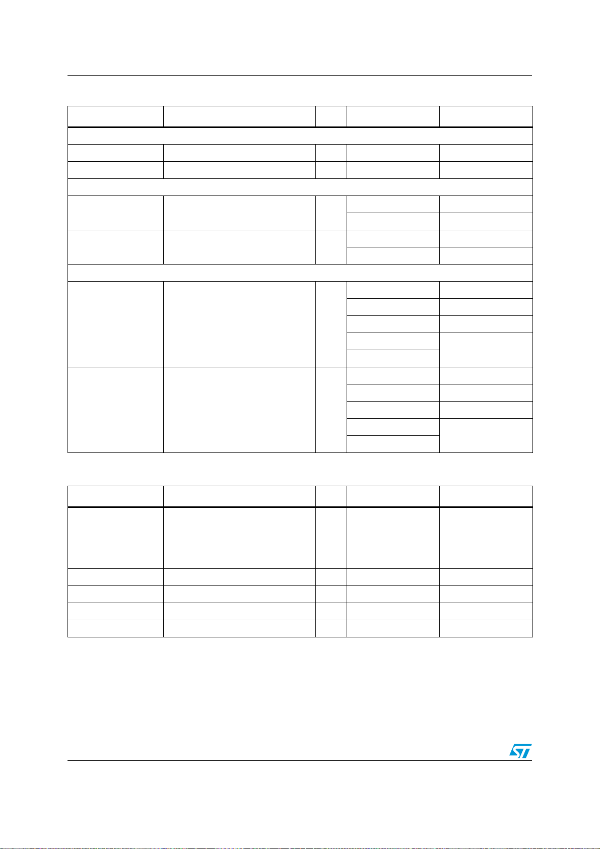
Pin description SPEAr320S
Table 28. I2C signals description
Signal name Description Dir. PL_GPIO_# /Ball Configuration mode
I2C0
I2C0_SCL I2C0 input/output clock IO PL_GPIO_4/C1 Alternate function
I2C0_SDA I2C0 input/output data IO PL_GPIO_5/D2 Alternate function
I2C1
PL_CLK2/J17 3
I2C1_SCL I2C1 input/output clock IO
PL_GPIO_8/C2 Extended mode
PL_CLK1/K17 3
I2C1_SDA I2C1 input/output data IO
PL_GPIO_9/B2 Extended mode
I2C2
PL_GPIO_2/E4 1
PL_GPIO_19/A3 2
I2C2_SCL I2C2 input/output clock IO
PL_GPIO_96/H15 4
PL_GPIO_75/E14
Extended mode
PL_GPIO_0/F3
PL_GPIO_3/D1 1
PL_GPIO_20/B4 2
I2C2_SDA I2C2 input/output data IO
PL_GPIO_97/H16 4
PL_GPIO_76/F13
Extended mode
PL_GPIO_1/E3
Table 29. I2S signals description
Signal name Description Dir. PL_GPIO_# /Ball Configuration mode
Audio oversampling clock. This is
the clock that I2S_CLK derives from.
audio_over_samp_clk
The interfacing digital-to-analog
O PL_GPIO_35/D8 1, 2
converter (DAC) can use this clock
to (over)sample the I2S data.
I2S_CLK I2S clock O PL_GPIO_39/A9 1, 2
I2S_LR I2S word select O PL_GPIO_40/B9 1, 2
I2S_RX I2S receive data I PL_GPIO_42/D9 1, 2
I2S_TX I2S transmit data O PL_GPIO_41/C9 1, 2
56/97 Doc ID 022508 Rev 1
Page 57
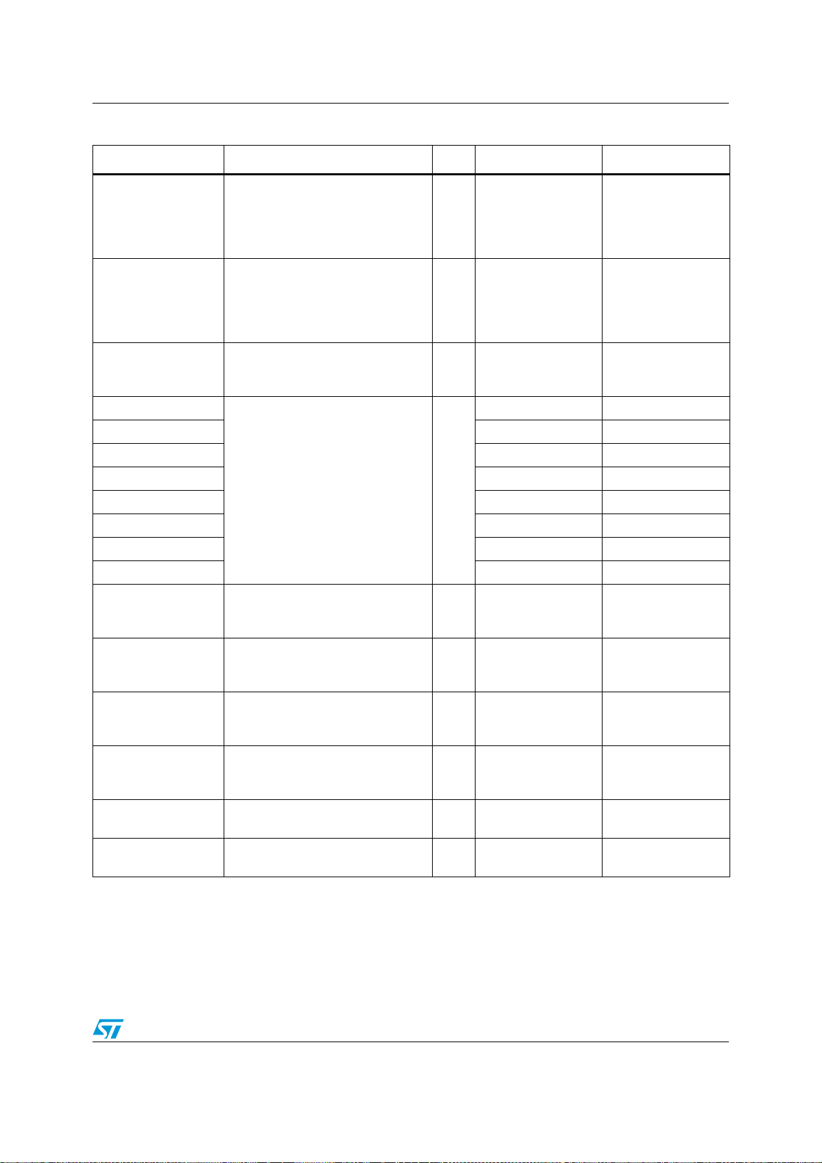
SPEAr320S Pin description
Table 30. SPP signals description
Signal name Description Dir. PL_GPIO_# /Ball Configuration mode
The peripheral pulses this line low
when it has received the previous
SPP_ACKn
data and is ready to receive more
O PL_GPIO_76/F13 4
data. The rising edge of SPP_ACKn
can be enabled to interrupt the host.
Usage of this line varies. Most
printers will perform a line feed after
SPP_AUTOFDn
each carriage return when this line
I PL_GPIO_72/B16 4
is low, and carriage returns only
when this line is high.
The peripheral drives this signal high
SPP_BUSY
to indicate that it is not ready to
O PL_GPIO_75/E14 4
receive data.
SPP_DATA0
PL_GPIO_85/F15 4
SPP_DATA1 PL_GPIO_84/D17 4
SPP_DATA2 PL_GPIO_83/E16 4
SPP_DATA3 PL_GPIO_82/E15 4
SPP unidirectional data lines O
SPP_DATA4 PL_GPIO_81/C17 4
SPP_DATA5 PL_GPIO_80/D16 4
SPP_DATA6 PL_GPIO_79/F14 4
SPP_DATA7 PL_GPIO_78/D15 4
Usage of this line varies. Peripherals
SPP_FAULTn
usually drive this line low when an
O PL_GPIO_71/D14 4
error condition exists.
This line is held low for a minimum of
SPP_INITn
50 µs to reset the printer and clear
I PL_GPIO_70/C15 4
the print buffer.
Usage of this line varies. Printers
SPP_PERROR
typically drive this signal high during
O PL_GPIO_74/C16 4
a paper empty condition.
The peripheral drives this signal high
SPP_SELECT
when it is selected and ready for
O PL_GPIO_73/A17 4
data transfer.
SPP_SELINn
SPP_STRBn
The host drives this line low to select
the peripheral.
Data is valid during an active low
pulse on this line.
I PL_GPIO_69/A16 4
I PL_GPIO_77/B17 4
Doc ID 022508 Rev 1 57/97
Page 58
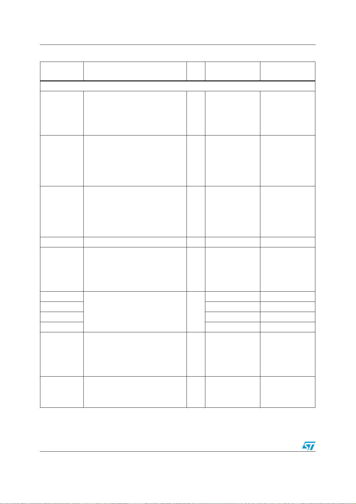
Pin description SPEAr320S
Table 31. Ethernet signals description
Signal name Description Dir.
MII0
PHY collision
This signal is asserted by the PHY when
MII0_COL
MII0_CRS
MII0_MDC
MII0_MDIO Management data input/output IO PL_GPIO_10/C3 Alternate function
MII0_RXCLK
a collision is detected on the medium.
This signal is not synchronous to any
clock.
(Active high)
PHY CRS
This signal is asserted by the PHY when
either the transmit or receive medium is
not idle. The PHY deasserts this signal
when both transmit and receive medium
are idle. This signal is not synchronous to
any clock. (Active high)
Management data clock
The MAC provides timing reference for
the MAC_MDIO signal through this
aperiodic clock. The maximum frequency
of this clock is 2.5 MHz.This clock is
generated from the application clock
(HCLK) via a clock divider.
Reception clock
This is the reception clock (25/2.5 MHz in
100M/10Mbps) provided by the external
PHY for MII interfaces. The MII0_RXDn
signals that the Ethernet controller
receives are synchronous to this clock.
I PL_GPIO_13/A1 Alternate function
I PL_GPIO_12/D4 Alternate function
O PL_GPIO_11/E5 Alternate function
I PL_GPIO_20/B4 Alternate function
PL_GPIO_# /
ball number
Configuration mode
(see Section 3.4.2)
MII0_RXD0
MII0_RXD1 PL_GPIO_16/E6 Alternate function
MII0_RXD2 PL_GPIO_15/B3 Alternate function
MII0_RXD3 PL_GPIO_14/A2 Alternate function
MII0_RXDV
MII0_RXER
58/97 Doc ID 022508 Rev 1
PHY receive data
These bits provide the MII receive data
nibble. The validity of the data is qualified
with MII0_RXDV and MII0_RXER.
PHY receive data valid
When high, indicates that the data on the
MII0_RXDn bus is valid. It remains
asserted continuously from the first
recovered byte/nibble of the frame
through the final recovered byte/nibble.
PHY receive error
When high, indicates an error or carrier
extension in the received frame on the
MII0_RXDn bus.
I
I PL_GPIO_19/A3 Alternate function
I PL_GPIO_18/D5 Alternate function
PL_GPIO_17/C4 Alternate function
Page 59
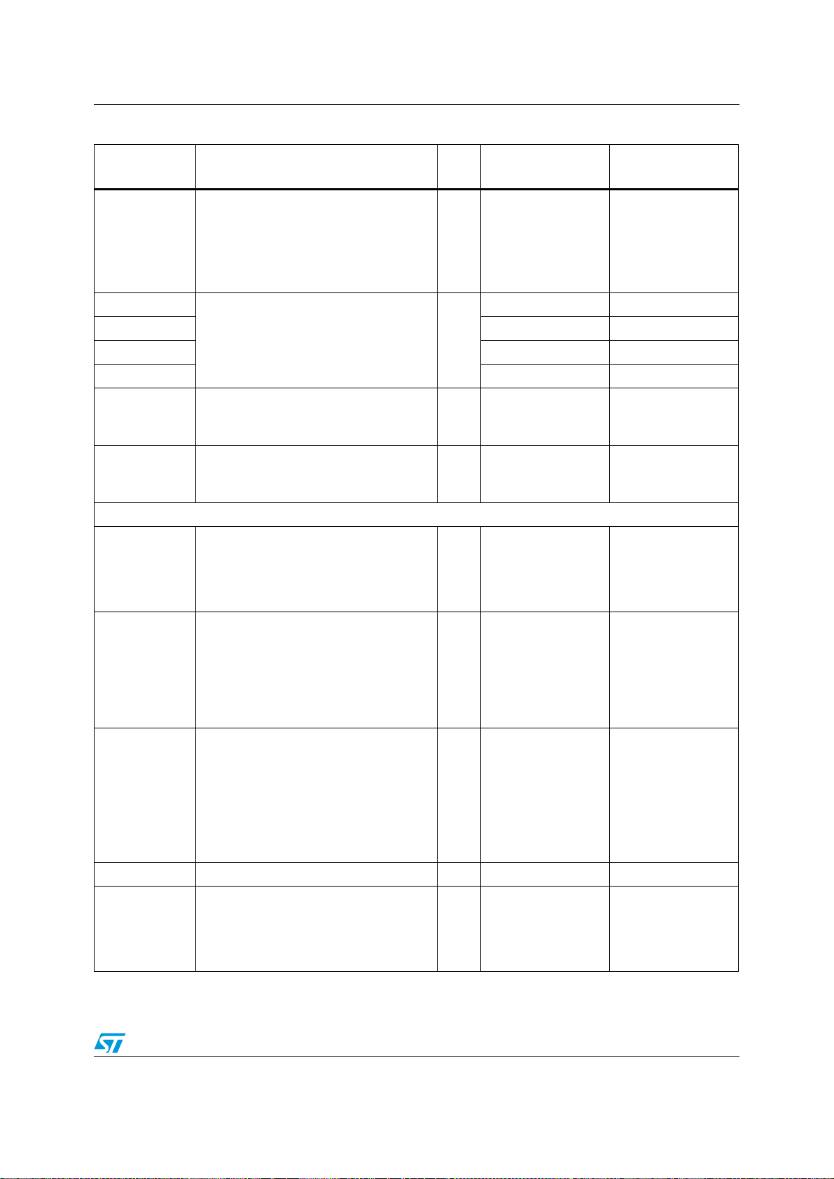
SPEAr320S Pin description
Table 31. Ethernet signals description (continued)
Signal name Description Dir.
Transmission clock
This is the transmission clock (25/2.5
MII0_TXCLK
MII0_TXD0 PHY transmit data.
MII0_TXD1 PL_GPIO_25/C6 Alternate function
MII0_TXD2 PL_GPIO_24/B5 Alternate function
MII0_TXD3 PL_GPIO_23/A4 Alternate function
MII0_TXEN
MII0_TXER
MII1
MII1_COL
MII1_CRS
MHz in 100 M/10 Mbps) provided by the
external PHY for the MII interface. All the
MII0_TXDn signals generated by the
MAC are synchronous to this clock.
These bits provide the MII transmit data
nibble. The validity of the data is qualified
with MII0_TXEN and MII0_TXER.
PHY transmit data enable
When high, it indicates that valid data is
being transmitted on the MII0_TXDn bus.
PHY transmit error
When high, indicates a transmit error or
carrier extension on the MII0_RXDn bus.
PHY collision
This signal is asserted by the PHY when
a collision is detected on the medium.
This signal is not synchronous to any
clock. (Active high)
PHY CRS
This signal is asserted by the PHY when
either the transmit or receive medium is
not idle. The PHY deasserts this signal
when both transmit and receive medium
are idle. This signal is not synchronous to
any clock. (Active high)
I PL_GPIO_27/B6 Alternate function
O
O PL_GPIO_22/D6 Alternate function
O PL_GPIO_21/C5 Alternate function
I PL_GPIO_83/E16 2
I PL_GPIO_82/E15 2
PL_GPIO_# /
ball number
PL_GPIO_26/A5 Alternate function
Configuration mode
(see Section 3.4.2)
Management data clock
The MAC provides timing reference for
the MII1_MDIO signal through this
MII1_MDC
MII1_MDIO Management data input/output IO PL_GPIO_81/C17 2
MII1_RXCLK
aperiodic clock. The maximum frequency
of this clock is 2.5 MHz.This clock is
generated inside the Ethernet controller
from the application clock (HCLK) via a
clock divider.
This is the reception clock (25/2.5 MHz in
100M/10Mbps) provided by the external
PHY for MII interfaces. All MII1_RXDn
signals that the Ethernet controller
receives are synchronous to this clock.
Doc ID 022508 Rev 1 59/97
O PL_GPIO_80/D16 2
I PL_GPIO_90/G14 2
Page 60
Pin description SPEAr320S
Table 31. Ethernet signals description (continued)
Signal name Description Dir.
MII1_RXD0
MII1_RXD1 PL_GPIO_86/E17 2
MII1_RXD2 PL_GPIO_85/F15 2
MII1_RXD3 PL_GPIO_84/D17 2
MII1_RXDV
MII1_RXER
MII1_TXCLK
PHY receive data
These bits provide the MII receive data
nibble. The validity of the data is qualified
with MII1_RXDV and MII1_RXER.
PHY receive data valid
When high, indicates that the data on the
MII1_RXDn bus is valid. It remains
asserted continuously from the first
recovered byte/nibble of the frame
through the final recovered byte/nibble.
PHY receive error
When high, indicates an error or carrier
extension in the received frame on the
MII1_RXDn bus.
Transmission clock
This is the transmission clock (25/2.5
MHz in 100M/10Mbps) provided by the
external PHY for the MII. All the MII
transmission signals generated by the
MAC are synchronous to this clock.
I
I PL_GPIO_89/F17 2
I PL_GPIO_88/F16 2
I PL_GPIO_97/H16 2
PL_GPIO_# /
ball number
PL_GPIO_87/G13 2
Configuration mode
(see Section 3.4.2)
MII1_TXD0 PHY transmit data.
MII1_TXD1 PL_GPIO_95/H14 2
MII1_TXD2 PL_GPIO_94/H13 2
MII1_TXD3 PL_GPIO_93/G17 2
MII1_TXEN
MII1_TXER
RMII0/RMII1
RMII_MDC
RMII_MDIO Management data input/output IO PL_GPIO_10/C3 Extended mode
RMII_REF_CLK
These bits provide the MII transmit data
nibble. The validity of the data is qualified
with MII1_TXEN and MII1_TXER.
PHY transmit data enable
When high, indicates that valid data is
being transmitted on the MII1_TXDn bus.
PHY transmit error
When high, indicates a transmit error or
carrier extension on the MII1_RXDn bus.
Management data clock
The MAC provides timing reference for
the RMII_MDIO signal through this
aperiodic clock. The maximum frequency
of this clock is 2.5 MHz.This clock is
generated from the application clock
(HCLK) via a clock divider.
50 MHz reference clock input for RMII
interface
O
O PL_GPIO_92/G16 2
O PL_GPIO_91/G15 2
O PL_GPIO_11/E5 Extended mode
I PL_GPIO_22/D6 Extended mode
PL_GPIO_96/H15 2
60/97 Doc ID 022508 Rev 1
Page 61
SPEAr320S Pin description
Table 31. Ethernet signals description (continued)
Signal name Description Dir.
PHY receive data valid
RMII0_CRS_DV
RMII0_RX_ER PHY receive error I PL_GPIO_13/A1 Extended mode
RMII0_RXD0 PHY receive data
RMII0_RXD1 PL_GPIO_15/B3 Extended mode
RMII0_TX_EN
RMII0_TXD0 PHY transmit data
RMII0_TXD1 PL_GPIO_17/C4 Extended mode
RMII1_CRS_DV
RMII1_RX_ER PHY receive error I PL_GPIO_18/D5 Extended mode
RMII1_RXD0 PHY receive data
RMII1_RXD1 PL_GPIO_20/B4 Extended mode
RMII1_TX_EN
RMII1_TXD0 PHY transmit data
RMII1_TXD1 PL_GPIO_21/C5 Extended mode
Contains the CRS (carrier sense) and
data valid information of the receive
interface.
These bits provide the RMII receive data.
The validity of the data is qualified with
RMII0_CRS_DV.
PHY transmit data enable
When high, indicates that valid data is
being transmitted on the RMII_TXDn bus
These bits provide the RMII transmit data.
The validity of the data is qualified with
RMII0_TX_EN.
PHY receive data valid
Contains the crs and data valid
information of the receive interface.
These bits provide the RMII receive data.
The validity of the data is qualified with
RMII1_CRS_DV.
PHY transmit data enable
When high, it indicates that valid data is
being transmitted on the RMII_TXDn bus.
These bits provide the RMII transmit data.
The validity of the data is qualified with
RMII1_TX_EN.
I PL_GPIO_14/A2 Extended mode
I
O PL_GPIO_16/E6 Extended mode
O
I PL_GPIO_19/A3 Extended mode
I
O PL_GPIO_23/A4 Extended mode
O
PL_GPIO_# /
ball number
PL_GPIO_26/A5 Extended mode
PL_GPIO_27/B6 Extended mode
PL_GPIO_24/B5 Extended mode
PL_GPIO_25/C6 Extended mode
Configuration mode
(see Section 3.4.2)
Doc ID 022508 Rev 1 61/97
Page 62
Pin description SPEAr320S
3.5 PL_GPIO pin sharing for debug modes
In some cases the PL_GPIO pins may be used in different ways for debugging purposes.
There are three different cases (see also
1. Case 1 - All the PL_GPIO get values from Boundary scan registers during Ex-test
instruction of JTAG . Typically, this configuration is used to verify the correctness of the
soldering process during the production flow.
2. Case 2 - All the PL_GPIO maintain their original meaning but the JTAG Interface is
connected to the processor. This configuration is useful during the development phase,
but offers only “static” debug.
3. Case 3 - Some PL_GPIOs, as shown in Table 32 below, are used to connect the ETM9
lines to an external box. This configuration is typically used only during the
development phase. It offers a very powerful debug capability. When the processor
reaches a breakpoint it is possible, by analyzing the trace buffer, to understand the
reason why the processor has reached the break.
Table 32. Ball sharing during debug
Signals Case 1 - no debug Case 2 - static debug Case 3 - full debug
TEST_0 0 1 0
TEST_1 0 0 1
Ta bl e 32):
TEST_2 0 0/1 0/1
TEST_3 0 0/1 0/1
TEST_4 1 0/1 0/1
nTRST nTRST_bscan nTRST_ARM nTRST_ARM
TCK TCK_bscan TCK_ARM TCK_ARM
TMS TSM_bscan TMS_ARM TSM_ARM
TDI TDI_bscan TDI_ARM TDI_ARM
TDO TDO_bscan TDO_ARM TDO_ARM
PL_GPIO_97 BSR Value Original meaning ARM_TRACE_CLK
PL_GPIO_96 BSR Value Original meaning ARM_TRACE_PKTA[0]
PL_GPIO_95 BSR Value Original meaning ARM_TRACE_PKTA[1]
PL_GPIO_94 BSR Value Original meaning ARM_TRACE_PKTA[2]
PL_GPIO_93 BSR Value Original meaning ARM_TRACE_PKTA[3]
PL_GPIO_92 BSR Value Original meaning ARM_TRACE_PKTB[0]
PL_GPIO_91 BSR Value Original meaning ARM_TRACE_PKTB[1]
PL_GPIO_90 BSR Value Original meaning ARM_TRACE_PKTB[2]
PL_GPIO_89 BSR Value Original meaning ARM_TRACE_PKTB[3]
PL_GPIO_88 BSR Value Original meaning ARM_TRACE_SYNCA
PL_GPIO_87 BSR Value Original meaning ARM_TRACE_SYNCB
PL_GPIO_86 BSR Value Original meaning ARM_PIPESTATA[0]
PL_GPIO_85 BSR Value Original meaning ARM_PIPESTATA[1]
62/97 Doc ID 022508 Rev 1
Page 63
SPEAr320S Pin description
Table 32. Ball sharing during debug (continued)
Signals Case 1 - no debug Case 2 - static debug Case 3 - full debug
PL_GPIO_84 BSR Value Original meaning ARM_PIPESTATA[2]
PL_GPIO_83 BSR Value Original meaning ARM_PIPESTATB[0]
PL_GPIO_82 BSR Value Original meaning ARM_PIPESTATB[1]
PL_GPIO_81 BSR Value Original meaning ARM_PIPESTATB[2]
PL_GPIO_80 BSR Value Original meaning ARM_TRACE_PKTA[4]
PL_GPIO_79 BSR Value Original meaning ARM_TRACE_PKTA[5]
PL_GPIO_78 BSR Value Original meaning ARM_TRACE_PKTA[6]
PL_GPIO_77 BSR Value Original meaning ARM_TRACE_PKTA[7]
PL_GPIO_76 BSR Value Original meaning ARM_TRACE_PKTB[4]
PL_GPIO_75 BSR Value Original meaning ARM_TRACE_PKTB[5]
PL_GPIO_74 BSR Value Original meaning ARM_TRACE_PKTB[6]
PL_GPIO_73 BSR Value Original meaning ARM_TRACE_PKTB[7]
PL_GPIO_[72:0]
Doc ID 022508 Rev 1 63/97
Page 64
Electrical characteristics SPEAr320S
4 Electrical characteristics
4.1 Absolute maximum ratings
This product contains devices to protect the inputs against damage due to high/low static
voltages. However, it is advisable to take normal precaution to avoid application of any
voltage higher/lower than the specified maximum/minimum rated voltages.
Caution: Stresses above those listed in Ta b l e 3 3 may cause permanent damage to the device.
Exposure to maximum rating conditions for extended periods may affect device reliability.
Table 33. Absolute maximum ratings
Symbol Parameter Min Max Unit
1.2 Supply voltage for the core - 0.3 1.44 V
V
DD
V
3.3 Supply voltage for the I/Os - 0.3 3.9 V
DD
2.5 Supply voltage for the analog blocks - 0.3 3 V
V
DD
V
1.8 Supply voltage for the DRAM interface - 0.3 2.16 V
DD
RTC RTC supply voltage -0.3 2.16 V
V
DD
T
STG
Storage temperature -55 150 °C
4.2 Maximum power consumption
Note: These values take into consideration the worst cases of process variation and voltage range
and must be used to design the power supply section of the board.
Table 34. Maximum power consumption
Symbol Description Max Unit
I
DD(1.2Vsupply)
I
DD(1.8Vsupply)
I
DD(RTC)
I
DD(2.5Vsupply)
I
DD(3.3Vsupply)
P
D
1. Peak current with Linux memory test (50% write and 50% read) plus DMA reading memory.
2. With 30 logic channels connected to the device and simultaneously switching at 10 MHz.
3. Based on bench measurements for worst case silicon under worst case operating conditions. Devices
tested with operating system running, CPU and DDR2 running at 333 MHz, DDR2 driven by PLL2,
SDRAM and all on-chip peripherals and internal modules enabled.
1.2 V current and power are primarily dependent on the applications running and the use of internal chip
functions (DMA, USB, Ethernet, and so on).
3.3 V current and power are primarily dependent on the capacitive loading, frequency, and utilization of the
external buses.
Current consumption of VDD 1.2 supply voltage for the core 400 mA
Current consumption of VDD 1.8 supply voltage for the
DRAM interface
(1)
150 mA
Current consumption of RTC supply voltage 8 µA
Current consumption of 2.5V supply voltage for the analog
blocks
Current consumption of 3.3V supply voltage for the I/Os
Maximum power consumption
(3)
(2)
30 mA
12 mA
870 mW
64/97 Doc ID 022508 Rev 1
Page 65
SPEAr320S Electrical characteristics
4.3 Recommended operating conditions
To ensure proper operation of the device, it is highly recommended to follow the conditions
shown in the following table.
Table 35. Recommended operating conditions
Symbol Parameter Min Typ Max Unit
V
1.2 Supply voltage for the core 1.14 1.2 1.3 V
DD
3.3 Supply voltage for the I/Os 3 3.3 3.6 V
V
DD
2.5 PLL supply voltage
V
DD
V
2.5 Oscillator supply voltage 2.25 2.5 2.75 V
DD
1.8 Supply voltage for DRAM interface 1.70 1.8 1.9 V
V
DD
RTC RTC supply voltage 1.3 1.5 1.8 V
V
DD
T
A
T
J
1. For power supply filtering it is required to add an external ferrite inductor.
2. TA to be considered under JESD51 conditions or equivalent ones.
Ambient temperature
Junction temperature -40 – 125 °C
(1)
(2)
2.25 2.5 2.75 V
-40 – 85 °C
4.4 Overshoot and undershoot
This product can support the following values of overshoot and undershoot.
Table 36. Overshoot and undershoot specifications
Parameter 3V3 I/Os 2V5 I/Os 1V8 I/Os
Amplitude 500 mV 500 mV 500 mV
Ratio of overshoot (or undershoot) duration with respect to
pulse width
1/3 1/3 1/3
If the amplitude of the overshoot/undershoot increases (decreases), the ratio of
overshoot/undershoot width to the pulse width decreases (increases). The formula relating
the two is:
Amplitude of OS/US = 0.75*(1- ratio of OS (or US) duration with respect to pulse width)
Note: The value of overshoot/undershoot should not exceed the value of 0.5 V. However, the
duration of the overshoot/undershoot can be increased by decreasing its amplitude.
4.5 3.3V I/O characteristics
The 3.3 V I/Os are compliant with JEDEC standard JESD8b.
Doc ID 022508 Rev 1 65/97
Page 66
Electrical characteristics SPEAr320S
Table 37. Low voltage TTL DC input specification (3 V< VDD <3.6 V)
Symbol Parameter Min Max Unit
V
V
V
hyst
Table 38. Low voltage TTL DC output specification (3 V< VDD <3.6 V)
Low level input voltage 0.8 V
IL
High level input voltage 2 V
IH
Schmitt trigger hysteresis 300 800 mV
Symbol Parameter Test condition Min Max Unit
V
V
OH
1. Maximum current load (IOL) = 10 mA for PL_GPIO and PL_CLK pins. For the IOL max value of dedicated
pins, refer to Chapter 3: Pin description.
Table 39. Pull-up and pull-down characteristics
Low level output voltage IOL= X mA
OL
High level output voltage IOH= -X mA
(1)
(1)
0.3 V
V
- 0.3 V
DD
Symbol Parameter Test condition Min Max Unit
R
R
Equivalent pull-up resistance VI = 0 V 29 67 kΩ
PU
Equivalent pull-down resistance VI = V
PD
3V3 29 103 kΩ
DDE
66/97 Doc ID 022508 Rev 1
Page 67
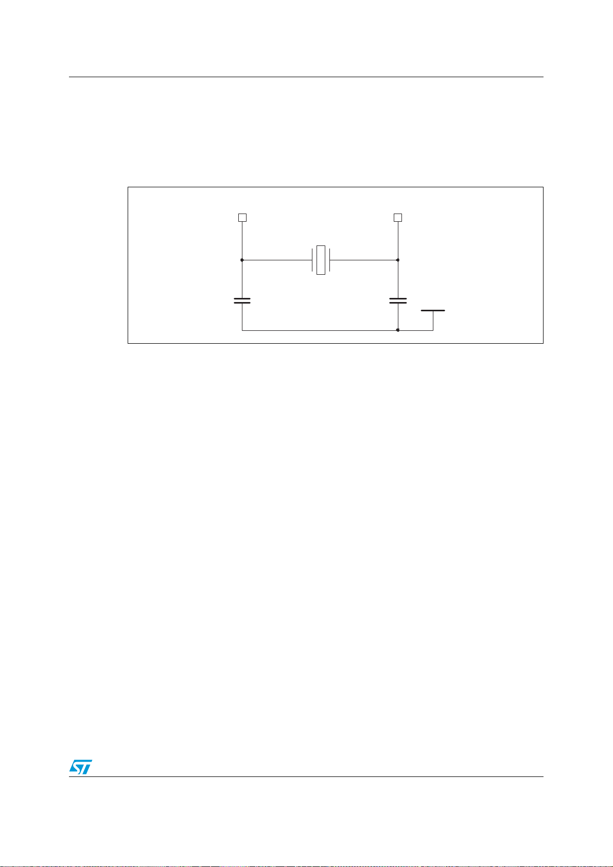
SPEAr320S Electrical characteristics
VDD2V5
24 MHz
CL1 CL2
(1)
(1)
MCLK_XI
MCLK_XO
4.6 Clocking parameters
4.6.1 Master clock (MCLK)
External clock generated from a crystal oscillator
Figure 4. MCLK crystal connection
1. CL1 and CL2 are the load capacitors.
The value of the capacitors depends on the type of the selected crystal. To calculate the
value of the load capacitance, use the formula given below.
For this example, Aker C2E-24.000-12-3030-X 24 MHz oscillator has been used.
Formula
CL = (CL1*CL2 / CL1+CL2) + CS
Where CL1 and CL2 are the load capacitors and CS is the circuit stray capacitance.
In our application:
CL1 = CL2 = Cext
This implies:
Cext = (CL-CS)*2
Example:
For the Aker C2E-24.000-12-3030-X crystal, CL = 12 PF
With CS = 3 PF, we have: Cext = CL1 = CL2 = 18 PF
Note: The ESR of the used quarz must be < 50 Ohm.
Doc ID 022508 Rev 1 67/97
Page 68
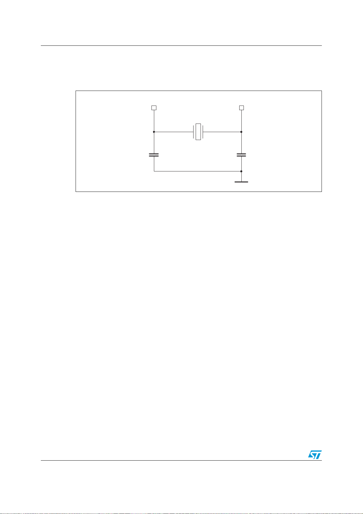
Electrical characteristics SPEAr320S
32.768 kHz
CL1 CL2
(1)
(1)
RTC_XI RTC_XO
4.6.2 Real-time clock (RTC)
External clock generated from a crystal oscillator
Figure 5. RTC crystal connection
GN D
1. CL1 and CL2 are the load capacitors.
The value of the capacitors depends on the type of the selected crystal. For example, using
Fox Electronics, P/N NC26LF-327 32.768 KHz oscillator, the value of the capacitors is
15
pF. The oscillator may not start if we use the crystal Fox fx325bs.
If the shunt capacitance (Co) of the crystal is ~7.0 pF, then the maximum ESR of the crystal
must be less than 50 Ohms.
68/97 Doc ID 022508 Rev 1
Page 69
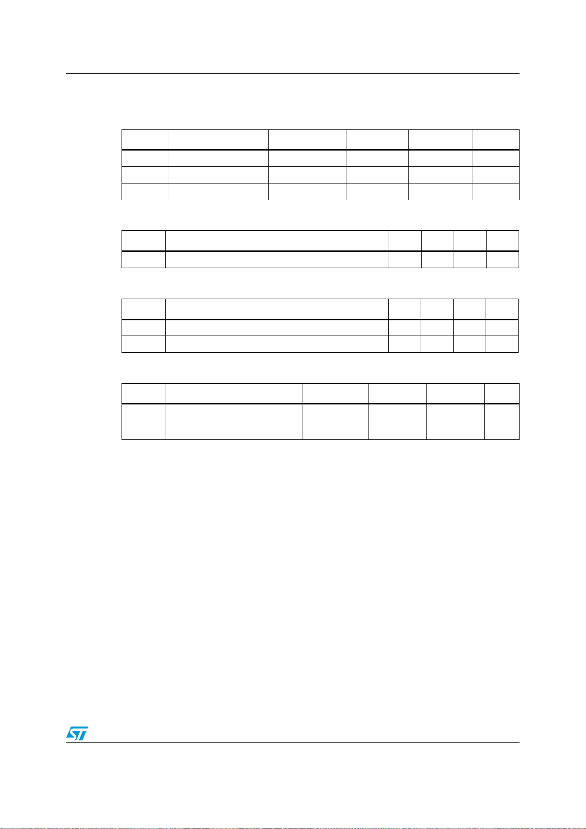
SPEAr320S Electrical characteristics
4.7 LPDDR and DDR2 pin characteristics
Table 40. DC characteristics
Symbol Parameter Test condition Min Max Unit
V
V
V
hyst
Table 41. Driver characteristics
Low level input voltage SSTL18 -0.3 V
IL
High level input voltage SSTL18 V
IH
+0.125 V
REF
-0.125 V
REF
1V8+0.3 V
DDE
Input voltage hysteresis 200 mV
Symbol Parameter Min Typ Max Unit
R
O
Table 42. On-die termination
Output impedance 45 Ω
Symbol Parameter Min Typ Max Unit
RT1 Termination value of resistance for on die termination 75 Ω
RT2 Termination value of resistance for on die termination 150 Ω
Table 43. Reference voltage
Symbol Parameter Min Typ Max Unit
V
REFIN
Voltage applied to core/pad 0.49 * V
DDE
0.500 * V
0.51 * V
DDE
DDE
V
Doc ID 022508 Rev 1 69/97
Page 70
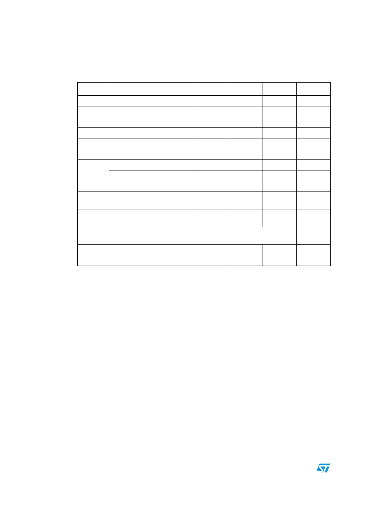
Electrical characteristics SPEAr320S
4.8 ADC pin characteristics
Table 44. ADC pin characteristics
Symbol Parameters Min Typ Max Unit
f
ADC_CLK
AV
DD
V
REFP
V
REFN
V
IREF
t
STARTUP
ADC_CLK frequency 3 14 MHz
ADC supply voltage 2.5 V
Positive reference voltage 2.5 V
Negative reference voltage 0 V
Internal reference voltage 1.95 2 2.05 V
Startup time 50 µs
Input range (absolute) AGND - 0.3 AVDD - 0.3 V
V
AIN
C
AIN
R
AIN
t
CONV
Conversion range V
REFN
Input capacitance 5 6.4 8 pF
Input mux resistance (total
equivalent sampling resistance)
1.5 2 2.5 KΩ
Conversion time
(f
ADC_CLK
=14 MHz)
V
REFP
1µs
Conversion time 13
INL Integral linearity error ±1 LSB
DNL Differential linearity error
±1 LSB
V
ADC_CLK
cycles
70/97 Doc ID 022508 Rev 1
Page 71
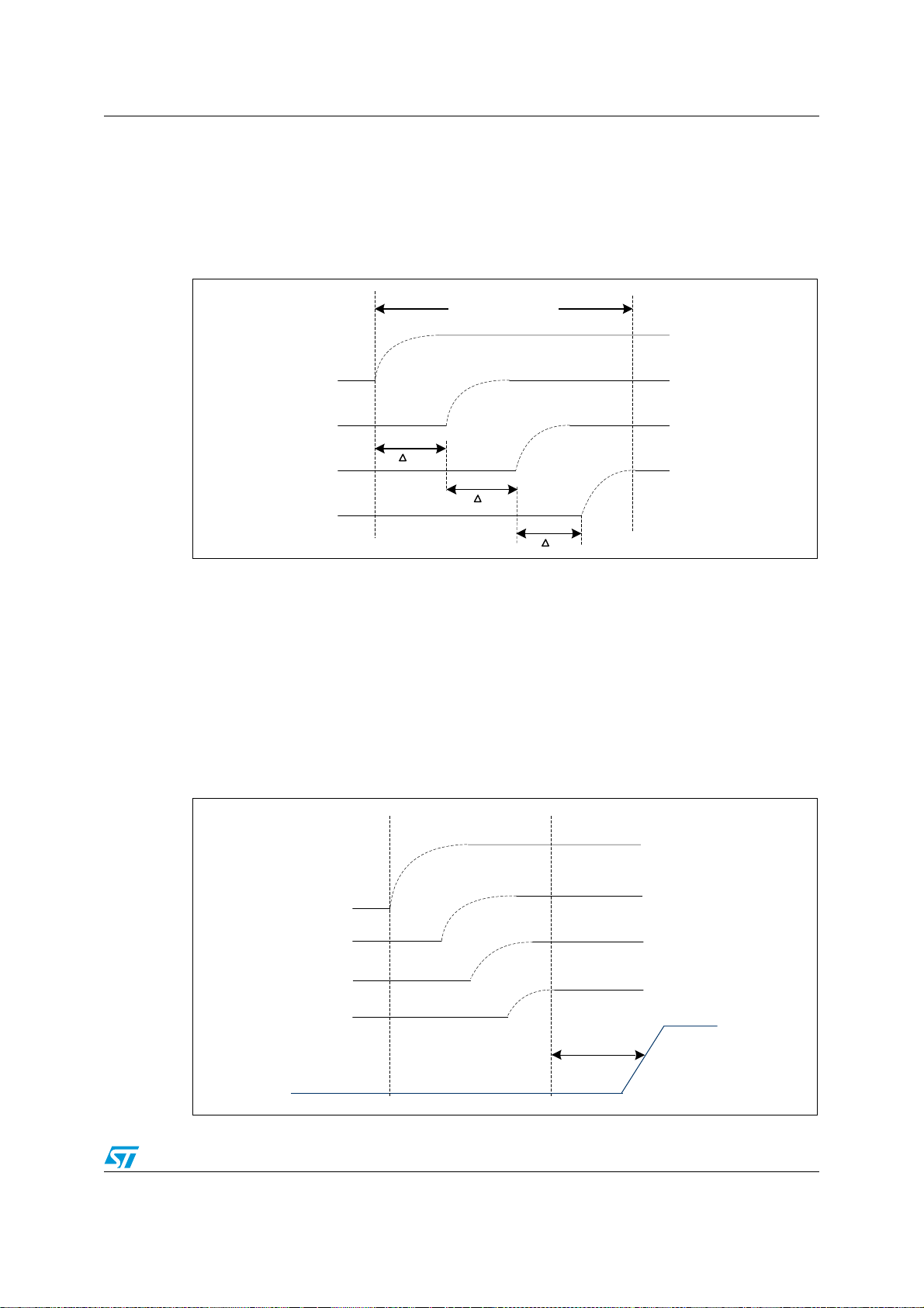
SPEAr320S Electrical characteristics
V
DD
1.2
V
DD
1.8
V
DD
2.5
V
DD
3.3
Power-up sequence
t
t
t
1V2
V3
1V8
MRESET
Start-up time= 2 ms
V5
4.9 Power-up sequence
It is recommended to power up the power supplies in the order shown in Figure 6.
VDD 1.2 is brought up first, followed by VDD 1.8, then VDD 2.5 and finally VDD 3.3. The minimum
time (
Δt) between each power up is >0 µs.
Figure 6. Power-up sequence
4.10 Power-down sequence
All power supplies can be shut down at the same time.
4.11 Reset release
The master reset (MRESET) must be released after all the power supplies are stable and for
a time interval of 2
Figure 7. Reset release
ms, which is the start-up time of the main oscillator.
V
DD
V
DD
V
2
DD
V
3
DD
Doc ID 022508 Rev 1 71/97
Page 72
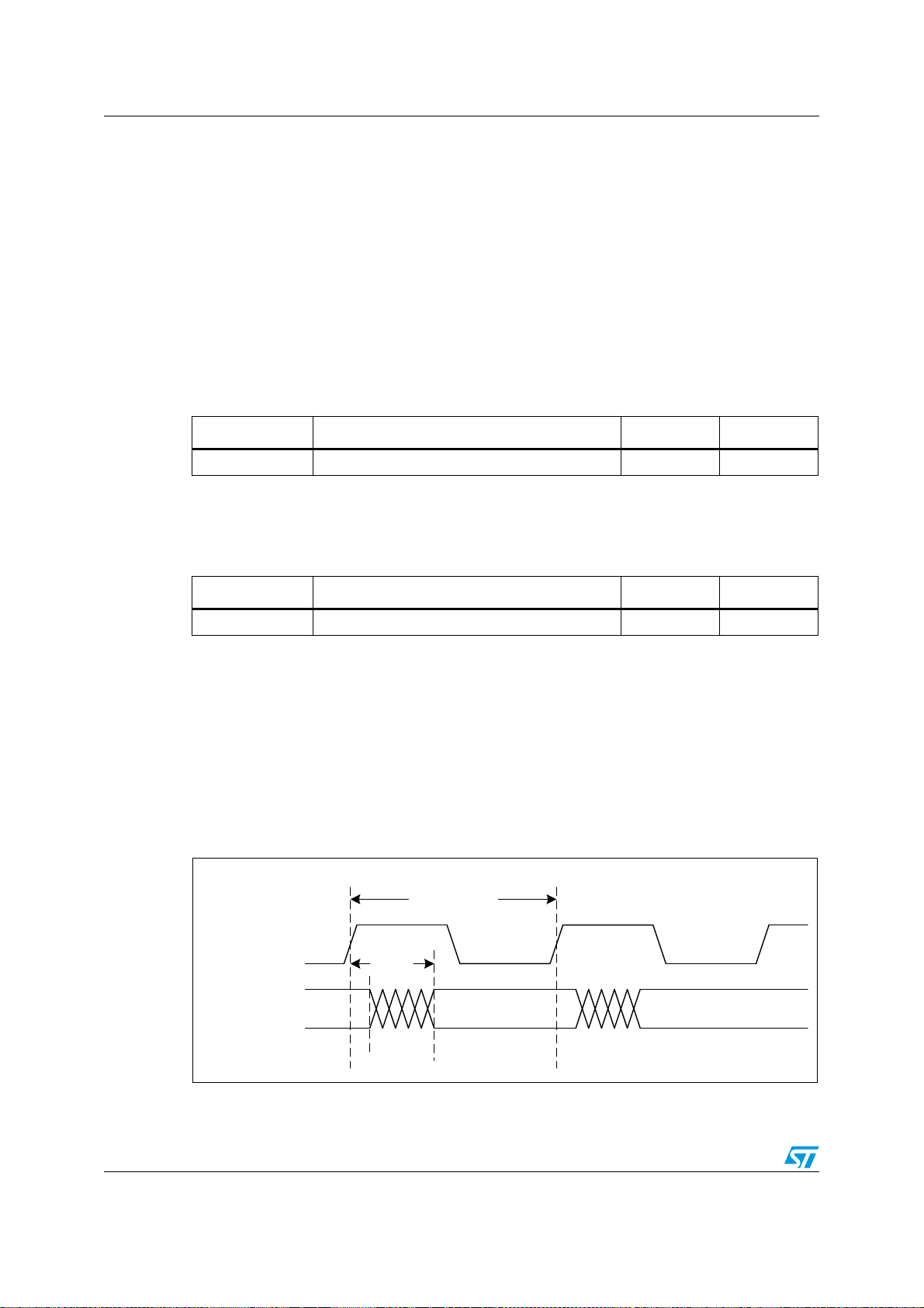
Timing requirements SPEAr320S
t
CK
t
D
CLD[23:0], CLAC,
CLLE, CLLP, CLFP,
CLPOWER
CLCP
5 Timing requirements
This chapter provides the timing requirements for the synchronous and asynchronous IPs
present in SPEAr320S.
The signal transition levels used for timing measurements are: 0.2*VDD and 0.8*VDD.
5.1 External interrupt timing characteristics
In legacy modes, all the interrupts are high-level triggered. In extended mode, interrupt
trigger polarity is programmable as rising or falling edge.
Table 45. PL_GPIO external interrupt input timing
Symbol Description Min Unit
tINT Minimum width for rising edge interrupt pulse 24 ns
5.2 Reset timing characteristics
Table 46. Cold reset (at power-on)
Symbol Description Min Unit
tRP MRESET pin active low state duration 10 ms
Note: Warm reset is generated by writing any value to the system controller SYSSTAT register.
5.3 CLCD timing characteristics
The CLCD has a wide variety of configurations, and the parameters change accordingly.
The timing characterization is performed assuming an output load capacitance of 10 pF on
all outputs.
Figure 8. CLCD waveform
72/97 Doc ID 022508 Rev 1
Page 73
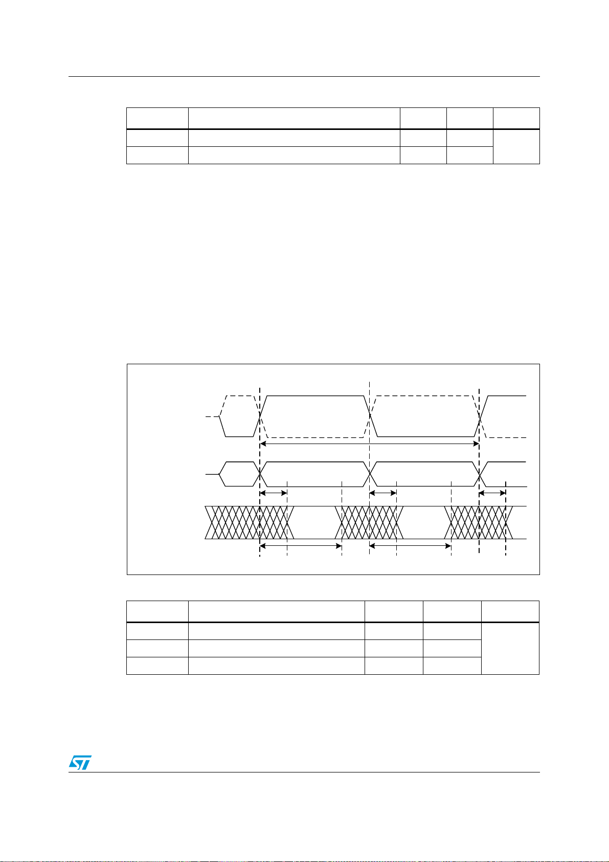
SPEAr320S Timing requirements
t
DQSQ
t
QH
t
QH
t
DQSQ
t
DQSQ
DDR_MEM_DQS_#
DDR_MEM_DQ_#
DDR_MEM_CLKP/
DDR_MEM_CLKN
t
CK
Table 47. CLCD timing requirements
Symbol Description Min Max Unit
t
CK
t
D
CLCP clock period 20.83 41.66
CLCP to CLCD output data delay 1 9.5
5.4 DDR2 timing characteristics
The timing parameters listed below are defined by the JEDEC Standard for DDR memories.
DDR memories whose parameters are within the ranges defined in
Ta bl e 50 can be interfaced with SPEAr320S.
Read cycle timing apply to DQS and DQ input to SPEAr. Write cycle timings refer to DQS
and DQ output to SPEAr.
The timing characterization is performed assuming an output load capacitance of 10 pF on
all the DDR pads.
5.4.1 DDR2 read cycle timing characteristics
Figure 9. DDR2 read cycle waveform
ns
Ta bl e 48, Ta bl e 49 and
Table 48. DDR2 read cycle timing requirements
Symbol Description Min Max Unit
t
CK
DQSQ
t
QH
DDR_MEM_CLKP/CLKN cycle time 3
DQS to DQ input setup time 0 0.25tCK+0.4
DQS to DQ input hold time 0.25tCK+0.7 0.5t
CK
Doc ID 022508 Rev 1 73/97
nst
Page 74
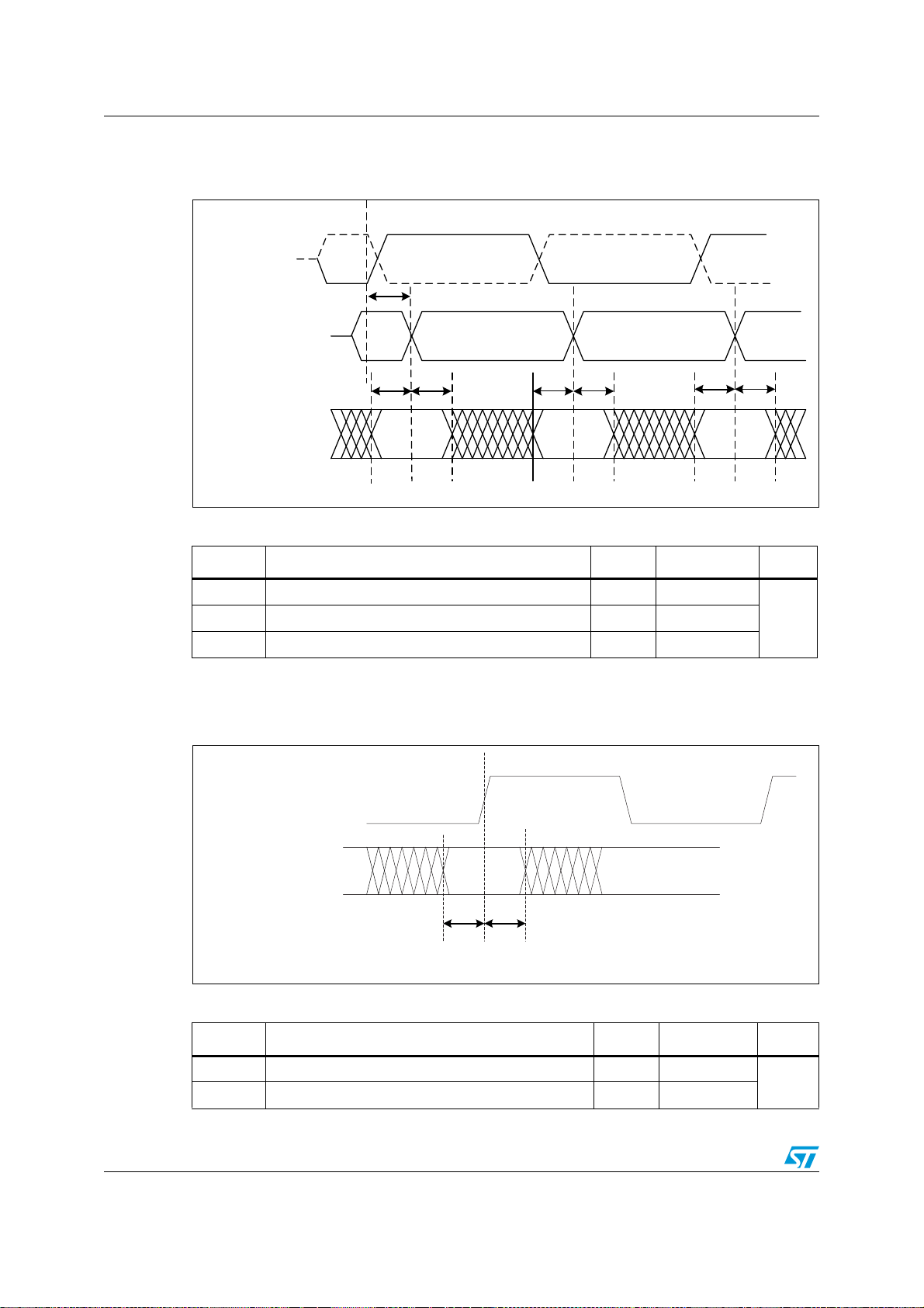
Timing requirements SPEAr320S
DDR_MEM_DQS_#
DDR_MEM_DQ_#
DDR_MEM_CLKP/
DDR_MEM_CLKN
t
DS
t
DH
t
DH
t
DS
t
DS
t
DH
t
DQSS
t
IStIH
CLK
Address and
commands
5.4.2 DDR2 write cycle timing characteristics
Figure 10. DDR2 write cycle waveform
Table 49. DDR2 write cycle timing requirements
Symbol Description Min Max Unit
t
DQSS
DS
t
DH
Positive DQS latching edge to associated CK edge -0.5 0.5
DQ & DQM output setup time relative to DQS 0 0.25tCK – 0.76
DQ & DQM output hold time relative to DQS 0 0.25tCK – 0.84
5.4.3 DDR2 command timing characteristics
Figure 11. DDR2 command waveform
Table 50. DDR2 command timing requirements
nst
Symbol Description Min Max Unit
t
t
Address and control output setup time 0 0.5tCK – 0.5
IS
Address and control output hold time 0 0.5tCK – 0.59
IH
74/97 Doc ID 022508 Rev 1
ns
Page 75
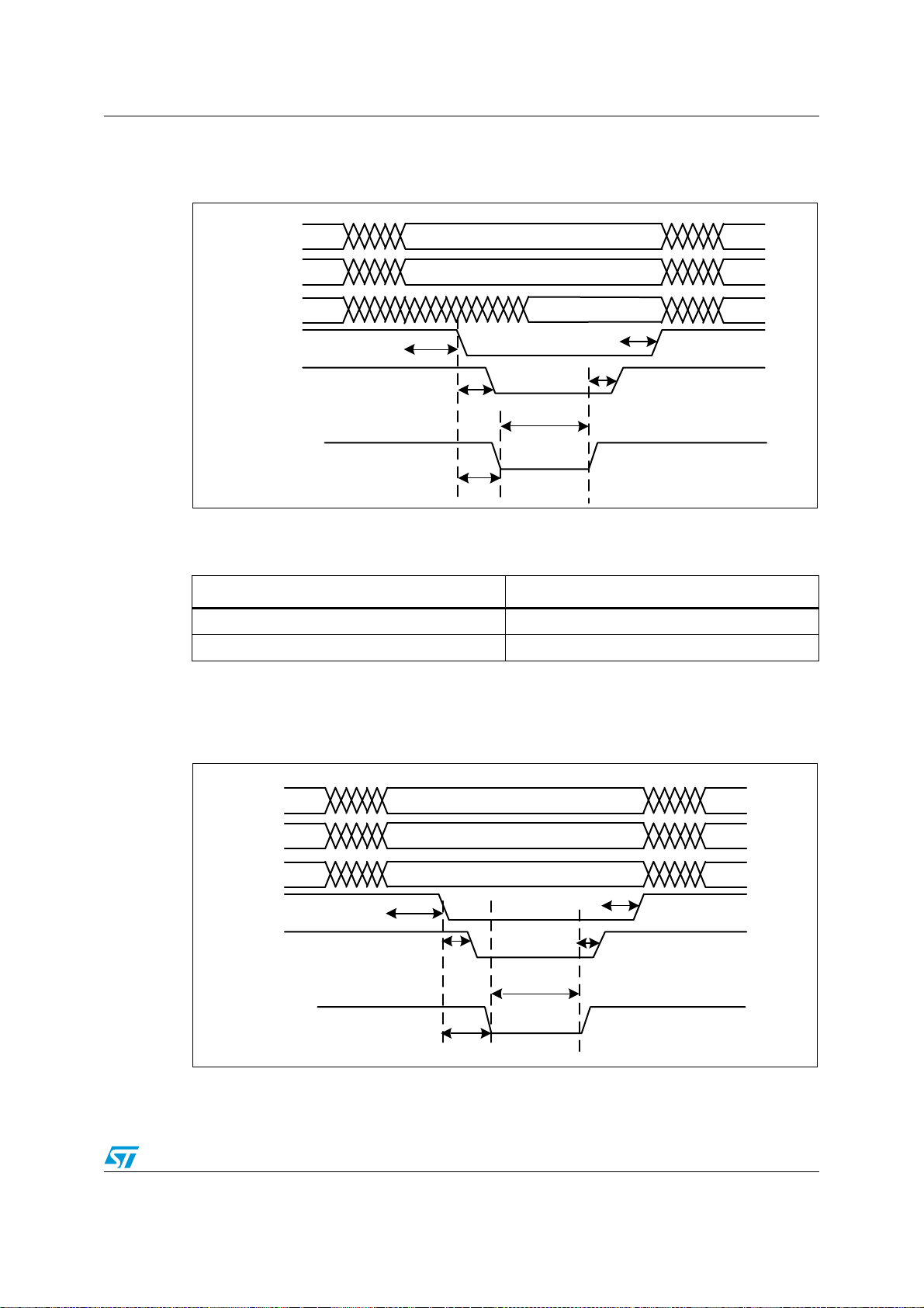
SPEAr320S Timing requirements
EMI_A#
EMI_BYTEN#
EMI_D#
EMI_CEn#
EMI_OE
Address
Byte Enable
Data
t
SE
t
SCS
t
ENr
t
DCS
EMI_WAIT
t
CS->Wait
t
WAIT
EMI_A#
EMI_BYTEN#
EMI_D#
EMI_CEn#
EMI_WE
Write Data
Byte Enable
Data
t
SE
t
SCS
t
ENw
t
DCS
EMI_WAIT
t
CS
->t
WAIT
t
WAIT
5.5 EMI timing characteristics
Figure 12. EMI read cycle waveform with acknowledgement on EMI_WAIT
Note: The values of tSE, t
Table 51. EMI timing requirements for read cycle with acknowledgement on WAIT
ENr
, t
DCS
, t
are programmable via the EMI registers.
SCS
Symbol Min
t
CS->Wait
t
WAIT
t
4*t
HCLK
HCLK
Note: Values in Ta bl e 51 refer to the common internal source clock which has a period of
t
= 6 ns.
HCLK
Figure 13. EMI write cycle waveform with acknowledgement on EMI_WAIT
Note: The values of tSE, t
ENw
, t
, t
DCS
are programmable via the EMI registers.
SCS
Doc ID 022508 Rev 1 75/97
Page 76
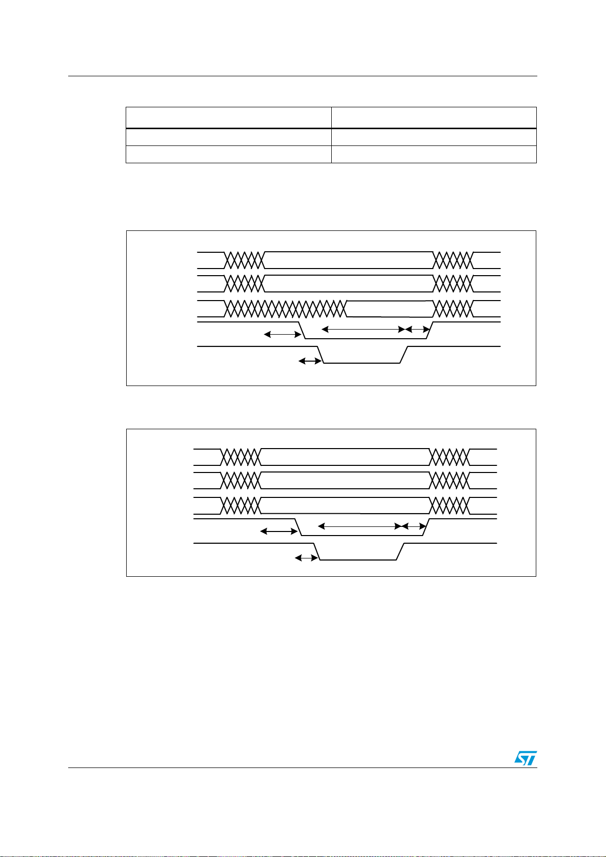
Timing requirements SPEAr320S
EMI_A#
EMI_BYTEN#
EMI_D#
EMI_CEn#
EMI_OE
Address
Byte Enable
Data
t
SE
t
SCS
t
ENr
t
DCS
EMI_A#
EMI_BYTEN#
EMI_D#
EMI_CEn#
EMI_WE
Write Data
Byte Enable
Data
t
SE
t
SCS
t
ENw
t
DCS
Table 52. EMI timing requirements for write cycle with acknowledgement on WAIT
Symbol Min
t
CS->Wait
t
WAIT
t
4*t
HCLK
HCLK
Note: Values in Ta bl e 52 refer to the common internal source clock which has a period of
t
= 6 ns.
HCLK
Figure 14. EMI read cycle waveform without acknowledgement on EMI_WAIT
Note: The values of tSE, t
ENr
, t
DCS
, t
are programmable via the EMI registers.
SCS
Figure 15. EMI write cycle waveform without acknowledgement on EMI_WAIT
Note: The values of tSE, t
76/97 Doc ID 022508 Rev 1
ENw
, t
, t
DCS
are programmable via the EMI registers.
SCS
Page 77
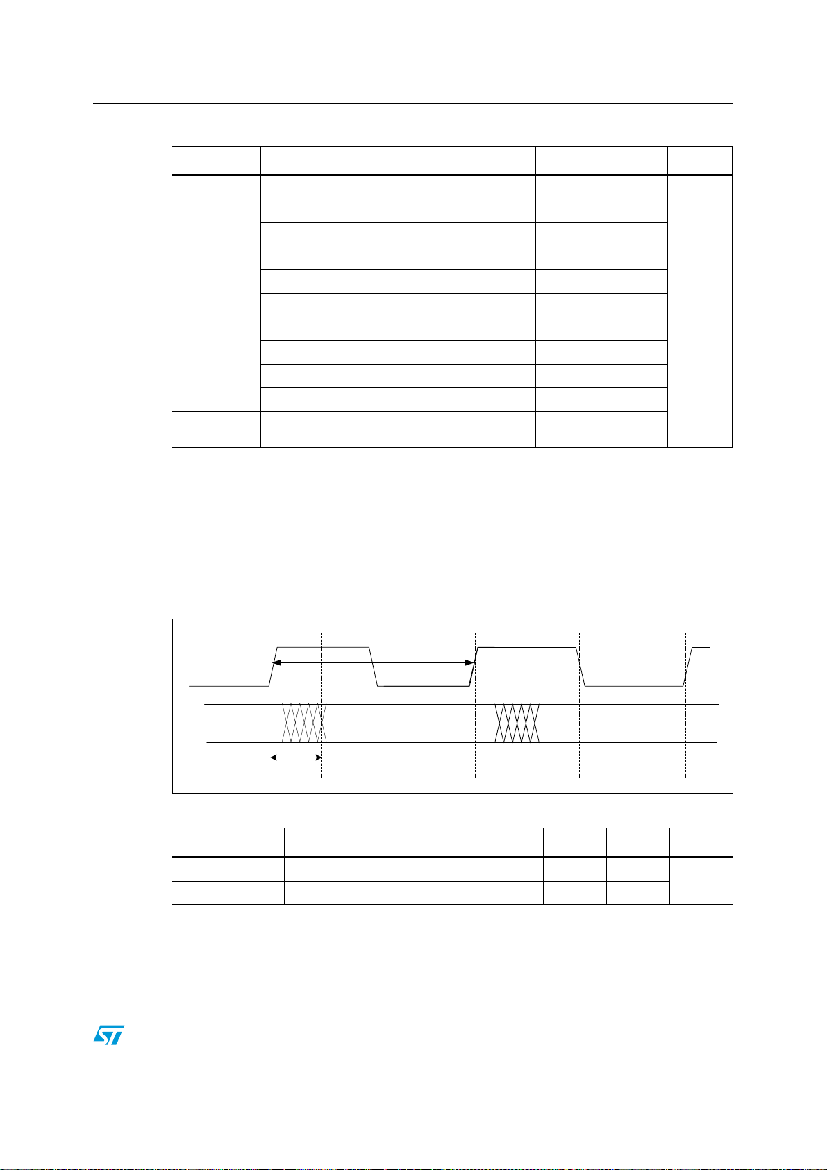
SPEAr320S Timing requirements
t
D
MII#_TXCLK
MII#_TXD0-MII#_TXD3,
MII#_TXEN, MII#_TXER
t
ck
Table 53. EMI timing requirements
Direction Signal name Max Min Unit
EMI_A0-EMI_A23 8.612293 1.93584
EMD0-EMID15 9.471291 2.260195
EMI_CE0 8.764648 2.90581
EMI_CE1 7.977348 2.636304
EMI_CE2 9.027624 2.930175
Output
EMI_CE3 9.29631 3.006315
EMI_BYTEN0 9.554388 3.092855
EMI_BYTEN1 9.233592 3.038856
EMI_RE 8.193018 2.680564
EMI_WE 8.172619 2.80189
ns
Input
EMI_D0-EMI_D15 10.8188 1.30245
5.6 Ethernet MII timing characteristics
The timing characterization is performed assuming an output load capacitance of 5 pF on
the MII TX clock (MII#_TXCLK) and 10 pF on the other pads.
5.6.1 MII transmit timing characteristics
Figure 16. MII TX waveform
Table 54. MII TX timing requirements
Symbol Description Min Max Unit
t
CK
t
D
Note: To calculate the t
you have to apply the following formula: t
MII#_TXCLK clock period 40 40
MII#_TXCLK to MII output data delay 3.34 11.86
value for the PHY, you have to consider the next tCK rising edge, so
SETUP
SETUP
= tCK - t
max
Doc ID 022508 Rev 1 77/97
ns
Page 78
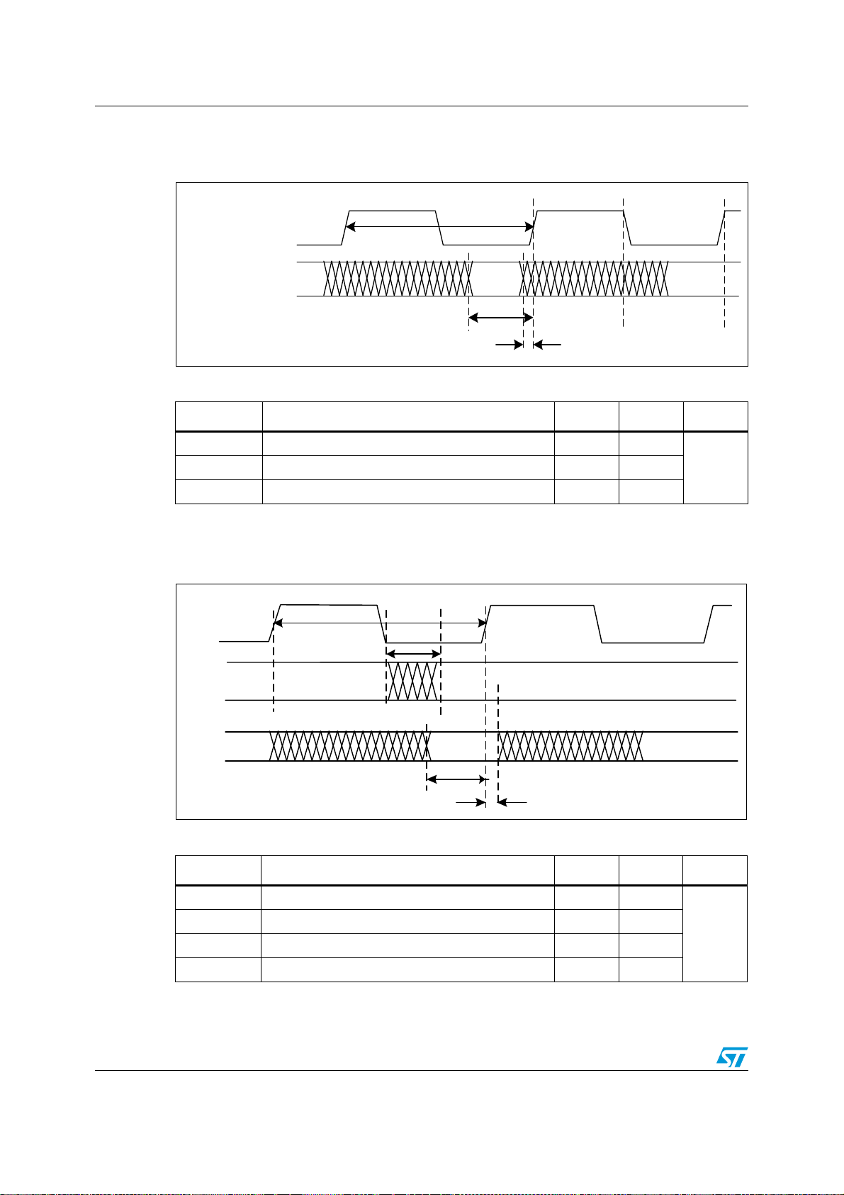
Timing requirements SPEAr320S
MII#_RXCLK
t
S
t
H
t
CK
MII#_RXD0-MII#_RXD3
MII#_RXER, MII#_RXDV
T
D
MDC
t
CK
t
H
t
S
MDIO(INPUT)
MDIO (OUTPUT)
5.6.2 MII receive timing characteristics
Figure 17. MII RX waveform
Table 55. MII RX timing requirements
Symbol Description Min Max Unit
t
CK
S
t
H
MII#_TXCLK clock period 40 40
Setup time requirement for MII receive data 12.5
Hold time requirement for MII receive data -2
5.6.3 MDIO timing characteristics
Figure 18. MDC waveform
Table 56. MDC timing requirements
nst
78/97 Doc ID 022508 Rev 1
Symbol Description Min Max Unit
t
CK
t
D
t
S
t
H
MDC clock period 614.4 614.4
Falling edge of MDC to MDIO output delay 204 0.64
Setup time requirement for MDIO input 9.6
Hold time requirement for MDIO input -6.6
ns
Page 79
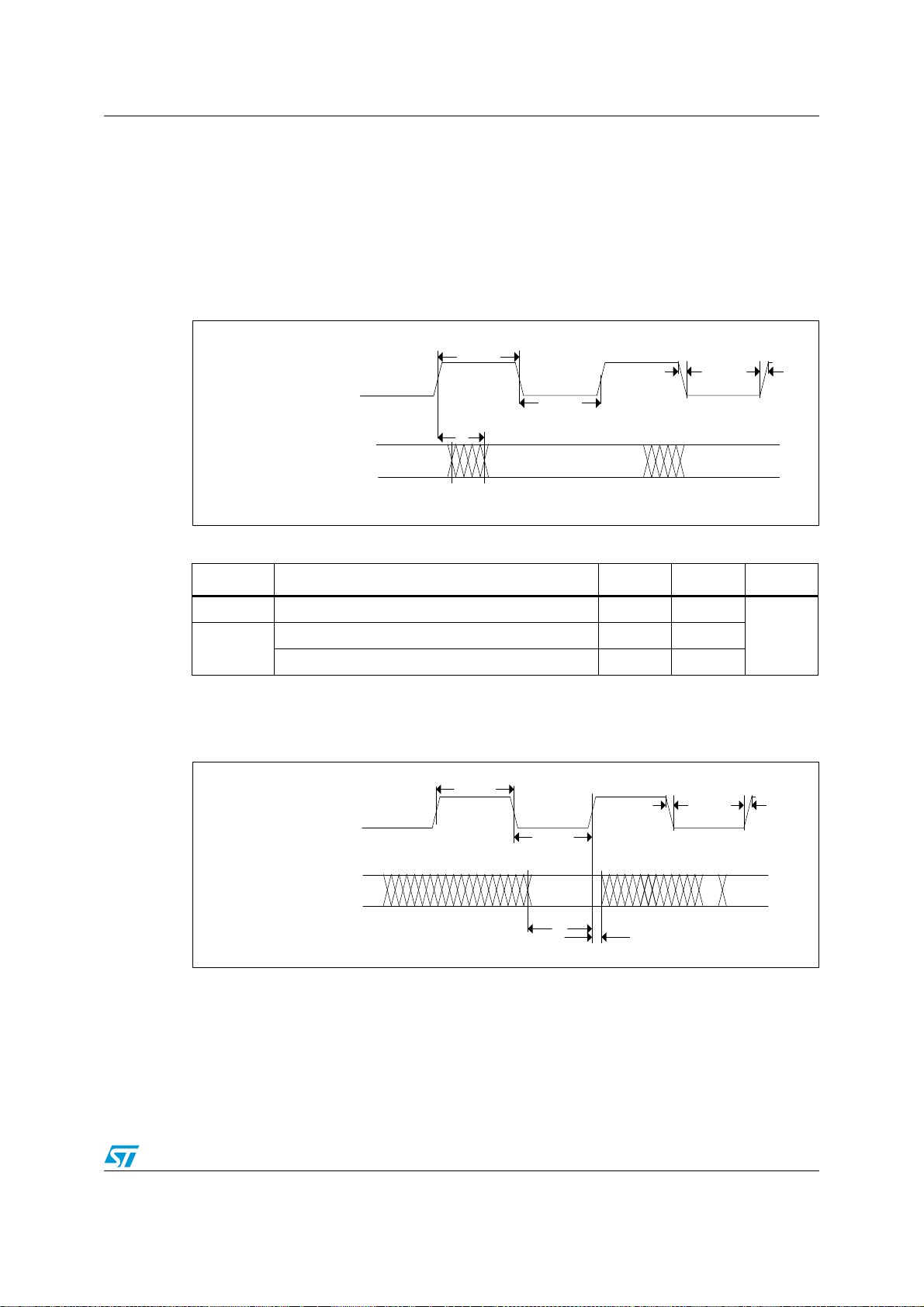
SPEAr320S Timing requirements
RMII_REF_CLK
RMIIn_TXD0, RMIIn_TXD1
RMIIn_TX_EN
Tf Tr
TCKhigh
TCKlow
TD
RMII_REF_CLK
Th
TCKhigh
TCKlow
Tf Tr
Ts
RMIIn_RXD0, RMIIn_RXD1
RMIIn_CRS_DV
Note: When MDIO is used as output the data are launched on the falling edge of the clock as
shown in
Figure 18.
5.7 Ethernet RMII timing characteristics
5.7.1 RMII transmit timing characteristics
Figure 19. RMII TX waveform
Table 57. RMII TX timing requirements
Symbol Description Min Max Unit
t
CK
RMII_REF_CLK period 20
Clock to RMII0_TXD output delay 2.95 9.5
t
D
Clock to RMII1_TXD output delay 2.95 9.3
5.7.2 RMII receive timing characteristics
Figure 20. RMII RX waveform
ns
Doc ID 022508 Rev 1 79/97
Page 80
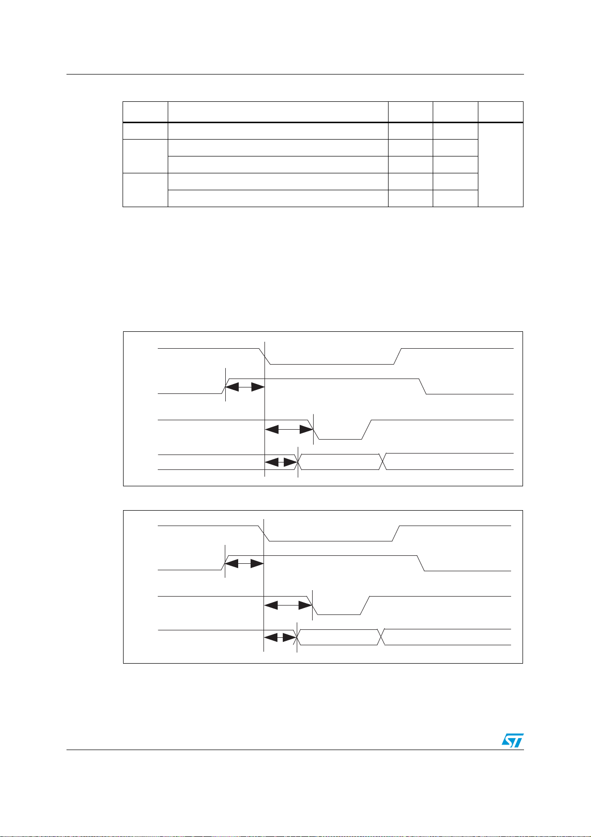
Timing requirements SPEAr320S
FSMC_CS#
FSMC_WE
FSMC_D#
Command
t
CLE
t
WE
t
IO
FSMC_CMD_LE
FSMC_ADDR_LE
FSMC_CS#
FSMC_WE
FSMC_D#
Address
t
ALE
t
WE
t
IO
Table 58. RMII RX timing requirements
Symbol Description Min Max Unit
t
RMII_REF_CLK period 20
CK
Setup time requirement for RMII0 receive data 4.9
t
S
Setup time requirement for RMII1 receive data 5
Hold time requirement for RMII0 receive data 0.1
t
H
Hold time requirement for RMII1 receive data -0.09
5.8 FSMC timing characteristics
The FSMC present in SPEAr320S can interface external parallel NAND Flash memories.
The timing characterization is performed using primetime assuming an output load
capacitance of 3
10
pF on FSMC_ADDR_LE and FSMC_CMD_LE.
Figure 21. Output command signal waveform
pF on the data, 15 pF on FSMC_CSx, FSMC_RE and FSMC_WE and
ns
Figure 22. Output address signal waveform
80/97 Doc ID 022508 Rev 1
Page 81
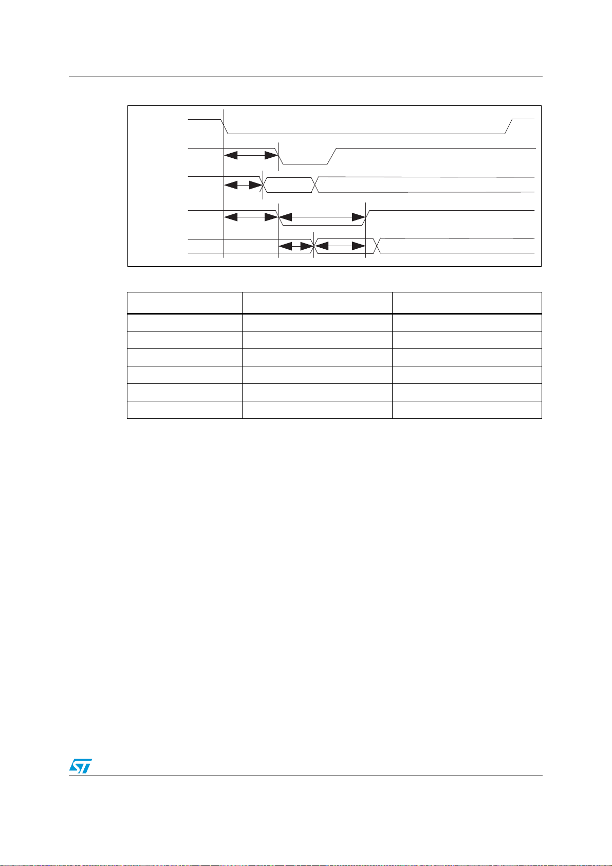
SPEAr320S Timing requirements
FSMC_CS#
FSMC_WE
FSMC_D# (out)
Data Out
t
IO
FSMC_D# (in)
FSMC_RE
t
RE -> IO
t
WE
t
RE
t
READ
t
NFIO -> FFs
Figure 23. In/out data address signal waveform
Table 59. FSMC timing requirements
Symbol Min Max
t
CLE
t
ALE
(1)
t
WE
(1)
t
RE
(2)
t
IO
(3)
t
READ
1. Programmable by the Tset bits in the FSMC registers.
2. Programmable by the Thiz bits in the FSMC registers.
3. Programmable by the Twait bits in the FSMC registers.
(((Tset+1) * t
(((Tset+1) * t
(((Thiz +1) * t
-3.9 2.8
-4.2 2.6
) - 3 ns) (((Tset+1) * t
HCLK
) - 3 ns) (((Tset+1) * t
HCLK
) - 3 ns) (((Thiz +1) * t
HCLK
((Twait+1)* t
HCLK
HCLK
HCLK
HCLK
) + 3 ns)
) + 3 ns)
)+ 3 ns)
Note: Values in Ta bl e 59 refer to the common internal source clock which has a period of t
ns.
HCLK
= 6
Doc ID 022508 Rev 1 81/97
Page 82
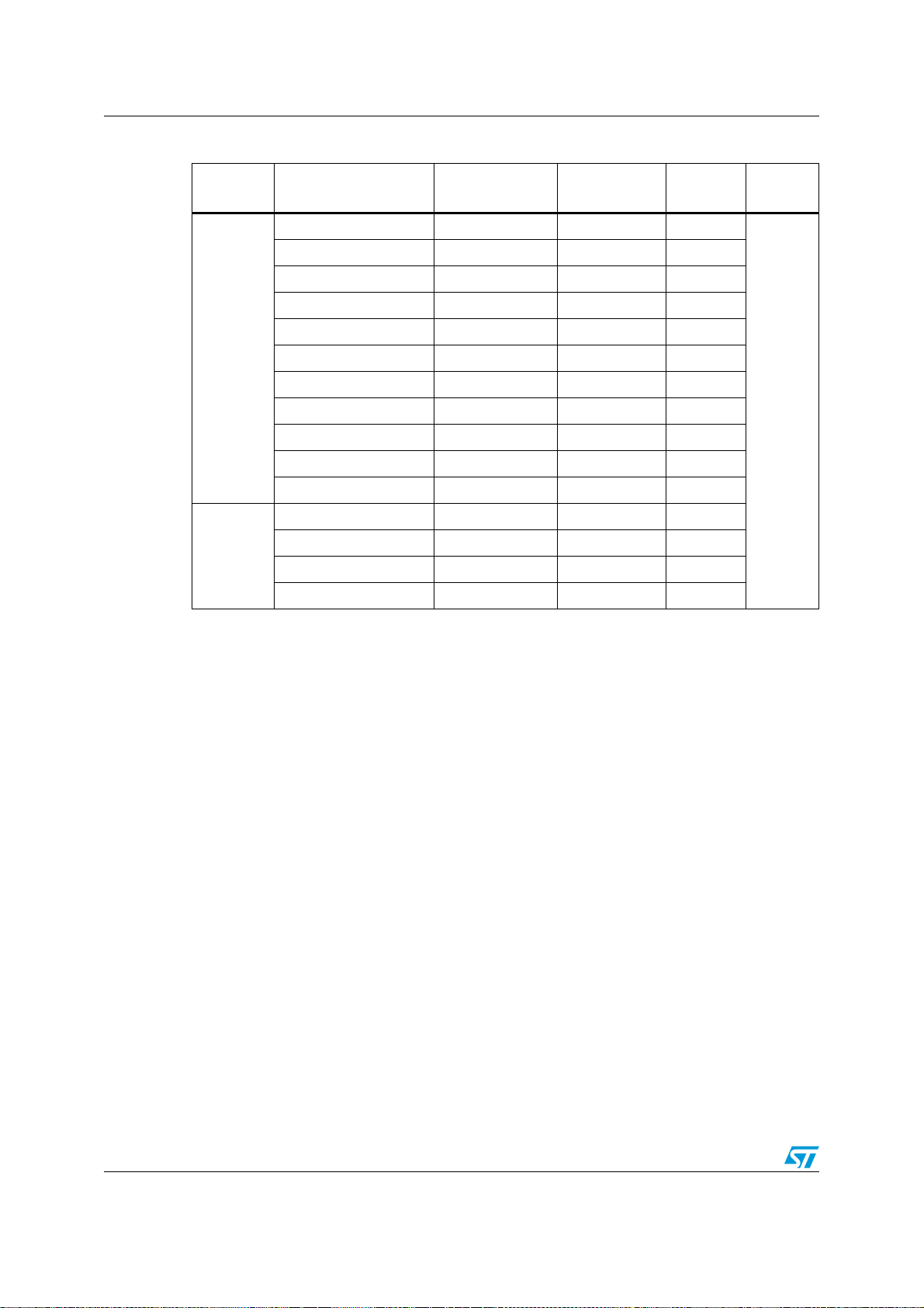
Timing requirements SPEAr320S
Table 60. FSMC signals timing requirements
Direction Signal name Max Min
FSMC_CMD_LE 10.57 3.1
FSMC_ADDR_LE 9.5 2.8
FSMC_WE 8.5 2.9
FSMC_RE 8.4 2.75
FSMC_CS0 9.165836 3.07661
FSMC_CS1 8.473722 2.81431
Output
FSMC_CS2 9.172739 3.02958
FSMC_CS3 9.808426 3.21934
FSMC_D7-FSMC_D0 7.710164 2.298715 8-bit
FSMC_D15-FSMC_D8 9.301547 2.420165 8-bit
FSMC_D15-FSMC_D0 9.301547 2.298715 16-bit
FSMC_RDY/BUSY 6.88 1.7
FSMC_D7-FSMC_D0 8.8809 1.18356 8-bit
Input
FSMC_D15-FSMC_D8 10.875302 1.37802 8-bit
FSMC_D15-FSMC_D0 10.875302 1.18356 16-bit
Data path
width
Unit
ns
82/97 Doc ID 022508 Rev 1
Page 83
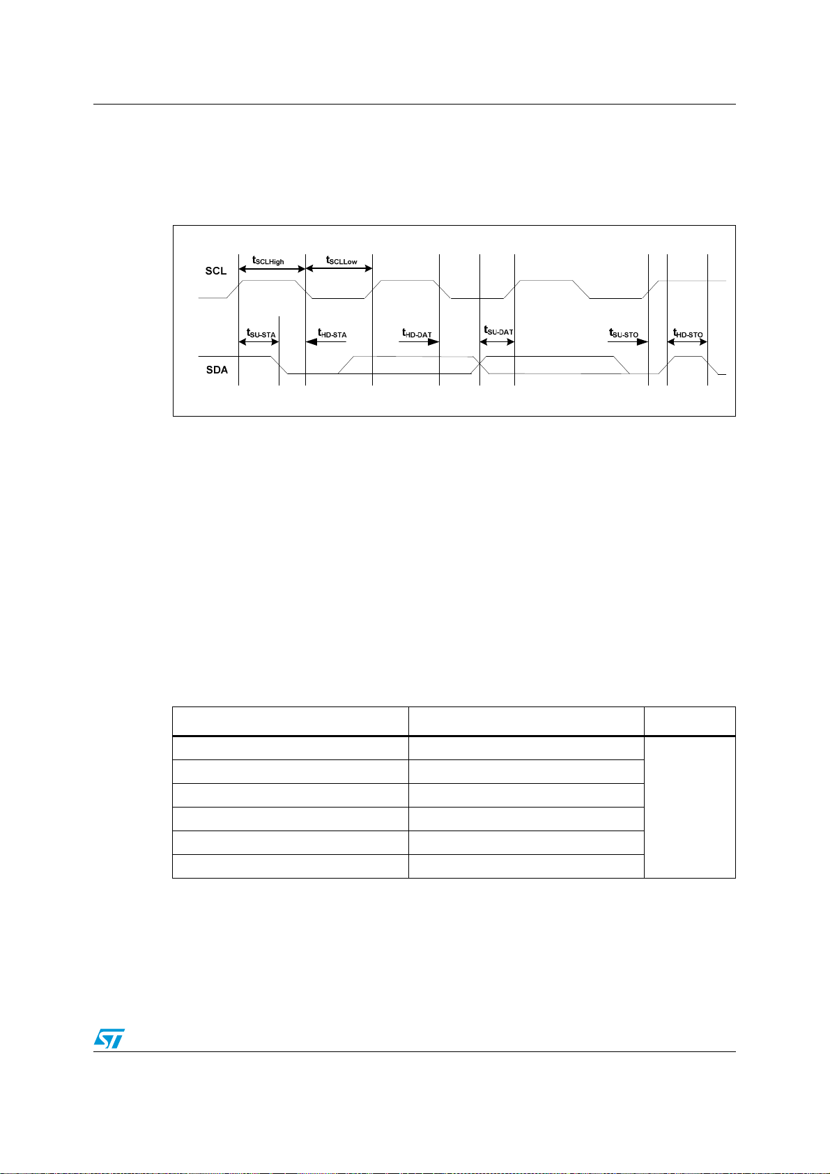
SPEAr320S Timing requirements
5.9 I2C timing characteristics
The timing characterization is performed using primetime assuming an output load
capacitance of 10 pF on SCL and SDA.
Figure 24. Output signal waveform for I2C signals
The timings of the high and low level of SCL (t
SCLHigh
and t
SCLLow
) are programmable.
The clock-to-output data delay is:
● MIN (T(clk+data)min) = 5.9
● MAX (T(clk+data)max) = 15
The timings shown in Figure 24 depend on the programmed value of t
SCLHigh
and t
SCLLow.
The values listed in Ta bl e 61 to Ta bl e 63 have been calculated using the minimum
programmable values of :
● High-speed mode: IC_HS_SCL_HCNT= 19 and IC_HS_SCL_LCNT= 53 registers
● Fast-speed mode: IC_FS_SCL_HCNT= 99 and IC_FS_SCL_LCNT= 215 registers
● Standard-speed mode: IC_SS_SCL_HCNT= 664 and IC_SS_SCL_LCNT=
780 registers
These minimum values depend on the AHB clock frequency, which is 166 MHz.
Table 61. I2C timing requirements in high-speed mode
Parameter Min Unit
t
SU-STA
t
HD-STA
t
SU-DAT
t
HD-DAT
t
SU-STO
t
HD-STO
140
325
300
ns
1
620
4745
Doc ID 022508 Rev 1 83/97
Page 84
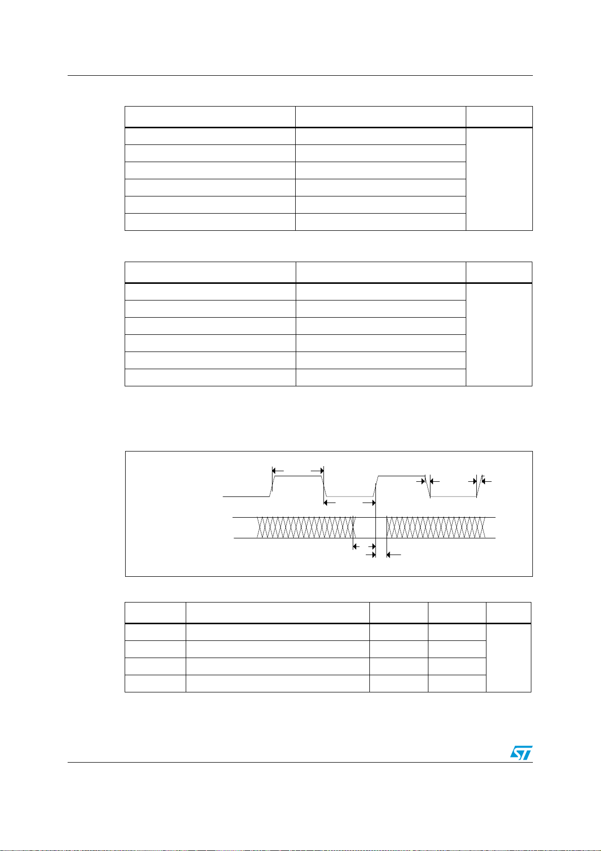
Timing requirements SPEAr320S
T
h
I2S_CLK
I2S_TX, I2S_LR
T
CKhigh
T
CKlow
T
s
T
f
T
r
Table 62. I2C timing requirements in fast-speed mode
Parameter Min Unit
t
SU-STA
t
HD-STA
t
SU-DAT
t
HD-DAT
t
SU-STO
t
HD-STO
Table 63. I2C timing requirements in standard-speed mode
Parameter Min Unit
t
SU-STA
t
HD-STA
t
SU-DAT
t
HD-DAT
t
SU-STO
t
HD-STO
5.10 I2S timing characteristics
620
602
1270
ns
1
620
4745
4718
3992
4660
ns
1
4010
4745
Figure 25. I2S waveform
Table 64. I2S timing requirements
Symbol Description Min Max Unit
t
CK
t
t
t
D
S
H
I2S_CLK clock period 40
I2S_CLK to I2S_TX output delay 3.8 9
Setup time requirement for I2S_CLK 6
Hold time requirement for I2S_CLK 1
ns
84/97 Doc ID 022508 Rev 1
Page 85
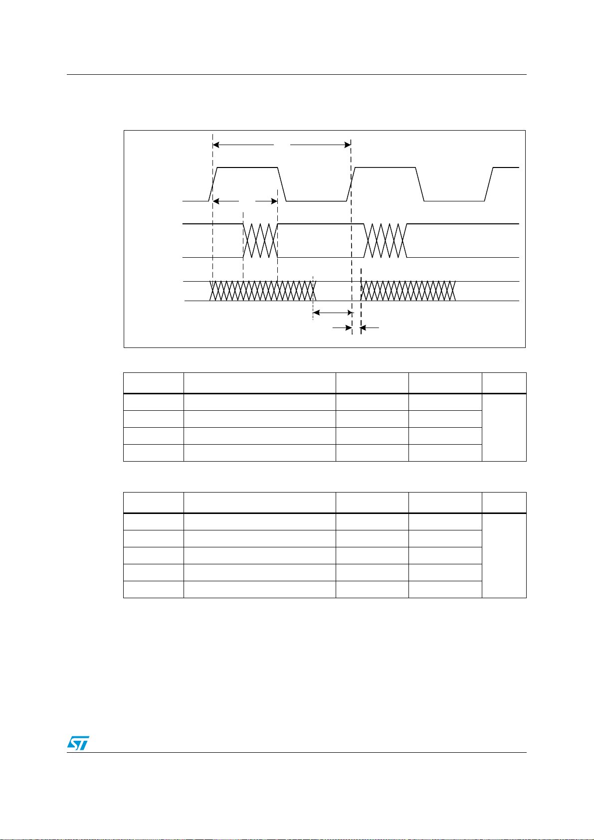
SPEAr320S Timing requirements
t
CK
SD_CLK
SD_DAT#
SD_WP
SD_CMD
SD_LED
SD_CD
SD_DAT#
(input)
t
S
t
H
D
t
5.11 SD timing characteristics
Figure 26. SD timing waveform
Table 65. SD timing requirements (high-speed mode, 48 MHz)
Symbol Description Min Max Unit
t
CK
t
D
t
S
t
H
Table 66. SD timing requirements (full-speed mode, 24 MHz)
SD_CLK clock period 20.8 –
SD_CLK to SD output delay -1.60 10
ns
Setup time requirement for SD inputs 7.35
Hold time requirement for SD inputs 0.19
Symbol Description Min Max Unit
t
CK
t
ck-half
t
t
t
D
S
H
SD_CLK clock period 41.6 –
SD_CLK half period 20.8
SD_CLK to SD output delay -0.40 10
Setup time requirement for SD inputs 7.35
Hold time requirement for SD inputs 0.19
ns
Note: In full-speed mode, the frequency is 24 MHZ (41.6 ns). The data is launched at the falling
edge of the 24
time is always 20.8
MHZ clock and captured on the clock’s rising edge (the effective available
ns)
Doc ID 022508 Rev 1 85/97
Page 86
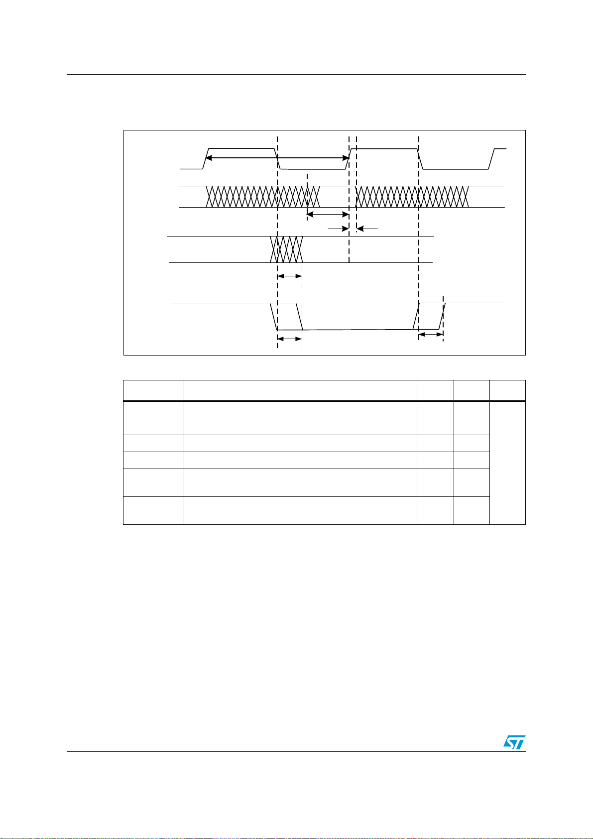
Timing requirements SPEAr320S
SMI_CLK
SMI_DATAIN
t
S
t
H
t
CK
t
D
t
CSf
t
CSr
SMI_DATAOUT
SMI_CS_0,1
5.12 SMI timing characteristics
Figure 27. SMI input/output waveform
Table 67. SMI timing requirements
Symbol Description Min Max Unit
t
CK
t
D
t
S
t
H
t
CSf
t
CSr
SMI clock period 20 50
SMI_CLK to SMI_DATAOUT output delay -2.96 3.05
Setup requirement for SMI_DATAIN 8.05
Hold requirement for SMI_DATAIN -2.53
Minimum and maximum delay of falling edge of
SMI_CS_0 , 1 with regard to SMI_CLK
Minimum and maximum delay of rising edge of
SMI_CS_0 , 1 with regard to SMI_CLK
-3.0 2.9
-2.8 2.8
ns
86/97 Doc ID 022508 Rev 1
Page 87
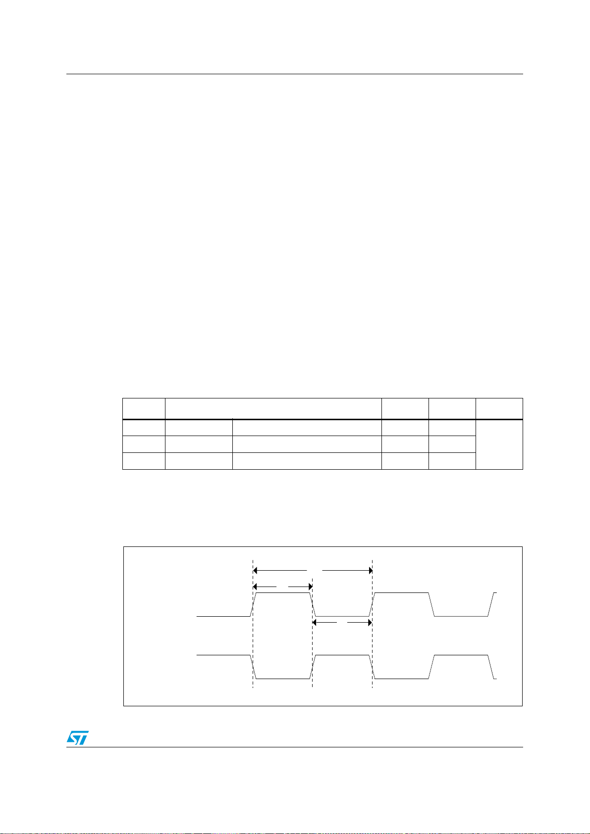
SPEAr320S Timing requirements
1
SSP#_CLK
(CPOL=0)
SSP#_CLK
(CPOL=1)
2
3
5.13 SSP timing characteristics
This module provides a programmable length shift register which allows serial
communication with other SSP devices through a 3- or 4-wire interface (SSP#_CLK,
SSP#_MISO, SSP#_MOSI and SSP#_CSn), where x= 0 to 2 and n= 1 to 4.
The SSP supports the following features related to timings:
● Master/Slave mode operation
● Chip-selects for interfacing multiple slave SPI devices.
● 3 or 4 wire interface (SSP_SCK, SSP_MISO, SSP_MOSI and SSP_CSn)
● Single interrupt
● Separate DMA events for SPI receive and transmit
● 16-bit shift register
● Receive buffer register
● Programmable character length (2 to 16 bits)
● Programmable SSP clock frequency range
● 8-bit clock pre-scaler
● Programmable clock phase (delay or no delay)
● Programmable clock polarity (CPOL)
Note: The following tables and figures show the characterization of the SSP using the SPI
protocol.
Table 68. SSP timing requirements (all modes)
(1)
No.
1T
3T
1. The number used in the graphics to represent the corresponding parameter.
c(CLK)
w(CLKH)
w(CLKL)
Parameters Min Max Unit
Cycle time, SSP#_CLK 24 –
Pulse duration, SSP#_CLK high 0.49*To 0.51*To
Pulse duration, SSP#_CLK low 0.49*To 0.51*To
T = Tc(CLK) = SSP#_CLK period is equal to the SSP module master clock divided by a
configurable divider.
Figure 28. SSP_CLK waveform
ns2T
Doc ID 022508 Rev 1 87/97
Page 88
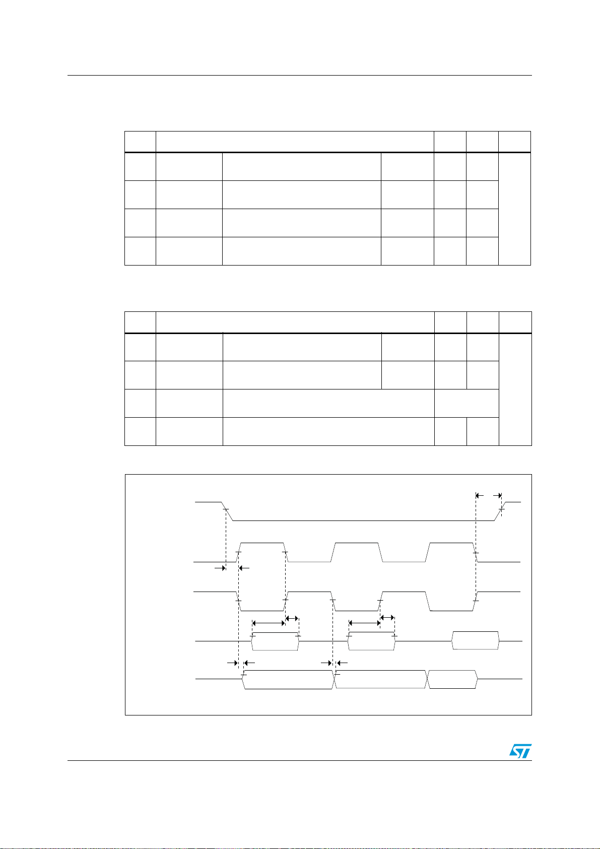
Timing requirements SPEAr320S
DATAMSB IN LSB IN
LSB OUTDATAMSB OUT
4
5
6
7
8
9
10
11
SSP#_CSn
SSP#_CLK
(CPOL=0)
SSP#_CLK
(CPOL=1)
SSP#_MISO
(input)
SSP#_MOSI
(output)
5.13.1 SPI master mode timing characteristics (clock phase = 0)
Table 69. SPI master mode timing requirements (clock phase = 0)
No. Parameters Min Max Unit
4t
su(DIV-CLKL)
5t
su(DIV-CLKH)
Setup time, MISO (input) valid before
SSP#_CLK (output) falling edge
Setup time, MISO (input) valid before
SSP#_CLK (output) rising edge
CPOL = 0 – 7.8
CPOL = 1 – 7.8
ns
6t
7t
Table 70. Switching characteristics over recommended operating conditions for
h(CLKL-DIV)
h(CLKH-DIV)
Hold time, MISO (input) valid after
SSP#_CLK (output) falling edge
Hold time, MISO (input) valid after
SSP#_CLK (output) rising edge
CPOL = 0 -2.7 –
CPOL = 1 -2.7 –
SPI master mode (clock phase =0 )
No. Parameters Min Max Unit
8t
d(CLKH-DOV)
9t
d(CLKL-DOV)
10 t
11 t
d(ENL-CLKH/L)
d(CLKH/L-ENH)
Delay time, SSP#_CLK (output) rising
edge to MOSI (output) transition
Delay time, SSP#_CLK (output) falling
edge to MOSI (output) transition
Delay time, SSP#_CSn (output) falling edge to first
SSP#_CLK (output) rising or falling edge
Delay time, SSP#_CLK (output) rising or falling
edge to SSP#_CSn (output) rising edge
CPOL = 0 2.7 9.4
CPOL = 1 2.7 9.4
ns
T
310
Figure 29. SPI master mode external timing waveform (clock phase = 0)
88/97 Doc ID 022508 Rev 1
Page 89
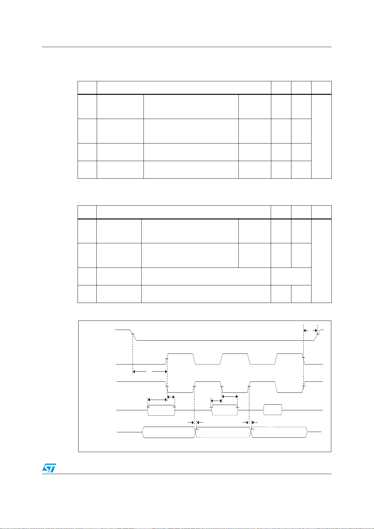
SPEAr320S Timing requirements
DATAMSB IN LSB IN
LSB OUTDATAMSB OUT
SSP#_CSn
SSP#_CLK
(CPOL=0)
SSP#_CLK
(CPOL=1)
SSP#_MISO
(input)
SSP#_MOSI
(output)
13
14
15 16
17
18
19
20
5.13.2 SPI master mode timing characteristics (clock phase = 1)
Table 71. SPI master mode timing requirements (clock phase = 1)
No. Parameters Min Max Unit
Setup time, MISO (input) valid
13 t
14 t
su(DIV-CLKL)
su(DIV-CLKH)
before SSP#_CLK (output) rising
edge
Setup time, MISO (input) valid
before SSP#_CLK (output) falling
edge
CPOL = 0 – 7.8
CPOL = 1 – 7.8
ns
15 t
16 t
Table 72. Switching characteristics over recommended operating conditions for
h(CLKL-DIV)
h(CLKH-DIV)
Hold time, MISO (input) valid after
SSP#_CLK (output) rising edge
Hold time, MISO (input) valid after
SSP#_CLK (output) falling edge
CPOL = 0 -2.7 –
CPOL = 1 -2.7 –
SPI master mode (clock phase = 1)
No. Parameters Min Max Unit
Delay time, SSP#_CLK (output)
17 t
d(CLKH-DOV)
falling edge to MOSI (output)
CPOL = 0 2.7 9.5
transition
Delay time, SSP#_CLK (output)
18 t
19 t
20 t
d(CLKL-DOV)
d(ENL-CLKH/L)
d(CLKH/L-ENH)
rising edge to MOSI (output)
CPOL = 1 2.7 9.5
transition
Delay time, SSP#_CSn (output) falling edge to first
SSP#_CLK (output) rising or falling edge
Delay time, SSP#_CLK (output) rising or falling
edge to SSP#_CSn (output) rising edge
ns
T/2
310
Figure 30. SPI master mode external timing waveform (clock phase = 1)
Doc ID 022508 Rev 1 89/97
Page 90

Timing requirements SPEAr320S
5.14 UART timing characteristics
No timing characterization has been performed for the UART. For information related to
baud rate generation, refer to:
● Section 2.12: Asynchronous serial ports (UART)
● RM0321, Reference manual, SPEAr320S address map and registers
90/97 Doc ID 022508 Rev 1
Page 91
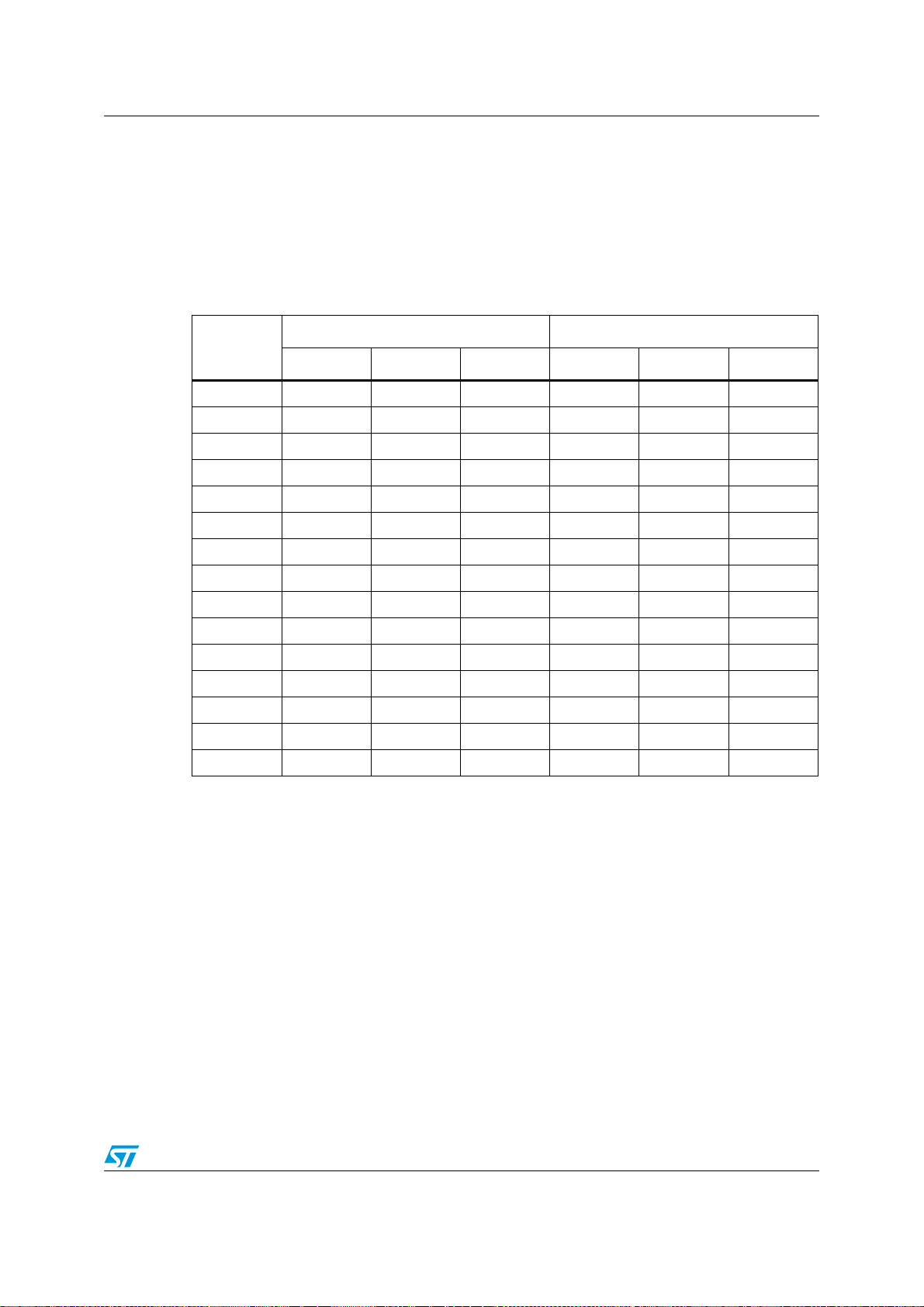
SPEAr320S Package information
6 Package information
In order to meet environmental requirements, ST offers these devices in different grades of
ECOPACK
specifications, grade definitions and product status are available at:
®
packages, depending on their level of environmental compliance. ECOPACK®
www.st.com.
ECOPACK® is an ST trademark.
Table 73. LFBGA289 (15 x 15 x 1.7 mm) mechanical data
mm inches
Dim.
Min. Type Max. Min. Type Max.
A 1.700 0.0669
A1 0.270 0.0106
A2 0.985 0.0387
A3 0.200 0.0078
A4 0.800 0.0315
b 0.450 0.500 0.550 0.0177 0.0197 0.0217
D 14.850 15.000 15.150 0.5846 0.5906 0.5965
D1 12.800 0.5039
E 14.850 15.000 15.150 0.5846 0.5906 0.5965
E1 12.800 0.5039
e 0.800 0.0315
F 1.100 0.0433
ddd 0.200 0.0078
eee 0.150 0.0059
fff 0.080 0.0031
Doc ID 022508 Rev 1 91/97
Page 92
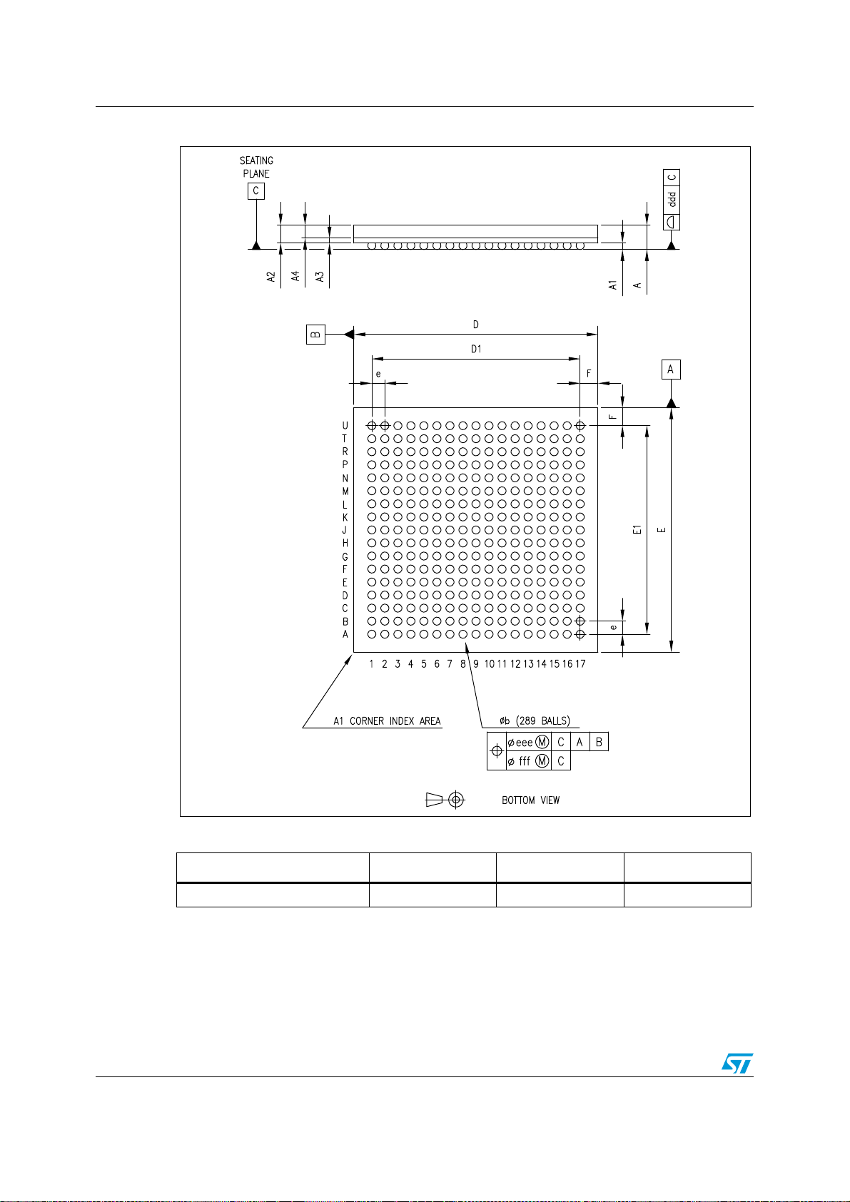
Package information SPEAr320S
Figure 31. LFBGA289 package dimensions
Table 74. Thermal resistance characteristics
Package Θ
JC
(°C/W)
LFBGA289 18.5 24.5 33
1. Measured on JESD51 2s2p test board.
92/97 Doc ID 022508 Rev 1
Θ
(°C/W) ΘJA(°C/W)
JB
(1)
Page 93
SPEAr320S Acronyms
Appendix A Acronyms
Table 75. List of acronyms
Acronym Definition
ADC Analog-to-digital converter
AES Advanced encryption standard
AHB AMBA high speed bus
AMBA Advanced microcontroller bus architecture
APB Advanced peripheral bus
BIST Built-In self test
CAN Controller area network
CBC Cipher block chaining
CMOS Complimentary metal-oxide semiconductor
CPU Central processing unit
CRC Cyclic redundancy check
DDR Double data rate
DES Data encryption standard
DLL Delay locked loop (when applied to DDR memories)
DMA Direct memory access
EMI External memory interface
ETM Embedded trace macrocell
FIFO First-in-first-out
FIQ Fast interrupt request
FPGA Field programmable gate array
FSMC Flexible static memory controller
GB Giga bytes
GPIO General purpose input / output
HLOS High-level operating system
HMI Human machine interface
HW Hardware
IrDA Infrared data association
IRQ Interrupt request
JPEG Joint photographic experts group
JTAG Joint test action group
KB Kilo bytes
LCD Liquid color display
Doc ID 022508 Rev 1 93/97
Page 94
Acronyms SPEAr320S
Table 75. List of acronyms (continued)
Acronym Definition
LSB Least significant bit
MAC Media access control
MB Mega bytes
MCU Microcontroller unit
MD5 Message digest 5
MII Media independent interface
MMU Memory management unit
MSB Most significant bit
PHY Physical (device, transceiver, layer)
PLL Phase locked loop
PWM Pulse width modulation
RAM Random access memory
RAS Reconfigurable array subsystem
RF Radio frequency
RFU Reserved for future use
RISC Reduced instruction set computing
RMII Reduced media independent interface
ROM Read only memory
RTC Real-time clock
RTOS Real-time operating system
RX Receive
SHA-1 Secure hash algorithm
SMI Serial memory interface
SoC System-on-chip
SPI Serial peripheral interface
SPP Standard parallel port
SRAM Static RAM
SSP Synchronous serial port
SW Software
TCM Tightly coupled memory
TFT Thin film transistor, a display technology
TX Transmit
UART Universal asynchronous receiver transmitter
USB Universal serial bus
94/97 Doc ID 022508 Rev 1
Page 95
SPEAr320S Acronyms
Table 75. List of acronyms (continued)
Acronym Definition
VIC Vectored interrupt controller
WDT Watchdog timer
Doc ID 022508 Rev 1 95/97
Page 96
Revision history SPEAr320S
Revision history
Table 76. Document revision history
Date Revision Changes
5-Apr-2012 1 Initial release.
96/97 Doc ID 022508 Rev 1
Page 97

SPEAr320S
Please Read Carefully:
Information in this document is provided solely in connection with ST products. STMicroelectronics NV and its subsidiaries (“ST”) reserve the
right to make changes, corrections, modifications or improvements, to this document, and the products and services described herein at any
time, without notice.
All ST products are sold pursuant to ST’s terms and conditions of sale.
Purchasers are solely responsible for the choice, selection and use of the ST products and services described herein, and ST assumes no
liability whatsoever relating to the choice, selection or use of the ST products and services described herein.
No license, express or implied, by estoppel or otherwise, to any intellectual property rights is granted under this document. If any part of this
document refers to any third party products or services it shall not be deemed a license grant by ST for the use of such third party products
or services, or any intellectual property contained therein or considered as a warranty covering the use in any manner whatsoever of such
third party products or services or any intellectual property contained therein.
UNLESS OTHERWISE SET FORTH IN ST’S TERMS AND CONDITIONS OF SALE ST DISCLAIMS ANY EXPRESS OR IMPLIED
WARRANTY WITH RESPECT TO THE USE AND/OR SALE OF ST PRODUCTS INCLUDING WITHOUT LIMITATION IMPLIED
WARRANTIES OF MERCHANTABILITY, FITNESS FOR A PARTICULAR PURPOSE (AND THEIR EQUIVALENTS UNDER THE LAWS
OF ANY JURISDICTION), OR INFRINGEMENT OF ANY PATENT, COPYRIGHT OR OTHER INTELLECTUAL PROPERTY RIGHT.
UNLESS EXPRESSLY APPROVED IN WRITING BY TWO AUTHORIZED ST REPRESENTATIVES, ST PRODUCTS ARE NOT
RECOMMENDED, AUTHORIZED OR WARRANTED FOR USE IN MILITARY, AIR CRAFT, SPACE, LIFE SAVING, OR LIFE SUSTAINING
APPLICATIONS, NOR IN PRODUCTS OR SYSTEMS WHERE FAILURE OR MALFUNCTION MAY RESULT IN PERSONAL INJURY,
DEATH, OR SEVERE PROPERTY OR ENVIRONMENTAL DAMAGE. ST PRODUCTS WHICH ARE NOT SPECIFIED AS "AUTOMOTIVE
GRADE" MAY ONLY BE USED IN AUTOMOTIVE APPLICATIONS AT USER’S OWN RISK.
Resale of ST products with provisions different from the statements and/or technical features set forth in this document shall immediately void
any warranty granted by ST for the ST product or service described herein and shall not create or extend in any manner whatsoever, any
liability of ST.
ST and the ST logo are trademarks or registered trademarks of ST in various countries.
Information in this document supersedes and replaces all information previously supplied.
The ST logo is a registered trademark of STMicroelectronics. All other names are the property of their respective owners.
© 2012 STMicroelectronics - All rights reserved
STMicroelectronics group of companies
Australia - Belgium - Brazil - Canada - China - Czech Republic - Finland - France - Germany - Hong Kong - India - Israel - Italy - Japan -
Malaysia - Malta - Morocco - Philippines - Singapore - Spain - Sweden - Switzerland - United Kingdom - United States of America
www.st.com
Doc ID 022508 Rev 1 97/97
 Loading...