

Page 1
Dual-core Cortex A9 HMI embedded MPU
PBGA (23 x 23 mm)
Features
■ CPU subsystem:
– 2x ARM Cortex A9 cores, up to 600 MHz
– 32+32 KB L1 caches per core, with parity
check
– Shared 512 KB L2 cache
– Accelerator coherence port (ACP)
■ Network-on-chip bus matrix, up to 166 MHz
■ 32 KB Boot ROM, 32+4 KB Static RAMs
■ Memory interfaces:
– DDR controller (DDR3-1066, DDR2-1066
@533MHz), 16-/32-bit, up to 2 GB address
space
– Serial NOR Flash controller
– Parallel NAND Flash/NOR Flash/SRAM
controller
■ Connectivity:
– 2 x USB 2.0 Host ports (integrated PHY)
– 1 x USB 2.0 OTG port (integrated PHY)
– 1 x Giga/Fast Ethernet port (external GMII/
RGMII/MII/RMII PHY)
– 1 x PCIe 2.0 RC/EP port (integrated PHY)
– 1 x 3Gb/s Serial ATA Host port (integrated
PHY)
– 1 x memory card interface: SD/SDIO/MMC,
CF/CF+, xD
– 2 x UART ports, with IrDA option
– 2 x I2C bus controllers, master/slave
– 1 x synchronous serial port,
SPI/Microwire/TI protocols, master/slave
– 2 x consumer electronic control (HDMI
CEC) ports
– 10-bit ADC: 8 ch. 1 Msps, with autoscan
– Programmable bidirectional GPIO signals
with interrupt capability
■ HMI support:
– LCD display controller, incl.support for Full
HD, 1920 x 1080, 60 Hz, 24 bpp
SPEAr1340
Datasheet − preliminary data
– High-perf. 2D/3D GPU, up to 1080p
– Hardware video decoder: multistandard up
to 1080p, JPEG
– Hardware video encoder: H.264 up to
1080p, JPEG
– Video input parallel port, with alternate
configuration for 4 x camera interfaces
– Digital audio ports: up to 7.1 multichannel
surround, I2S (8 in, 8 out) and S/PDIF
– 6 x 6 keyboard controller
– Resistive touchscreen interface
■ Security:
– Cryptographic co-processor: DES, 3DES,
AES, HMAC, PKA, RNG
– Secure boot support
– JTAG disable option
■ Miscellaneous functions:
– Energy saving: power islands, clock gating,
dynamic frequency scaling
– 2 x DMA controllers (total 16 channels)
– 11 x general purpose timers, 2 x watchdogs,
1 x real-time clock
– 4 x PWM generators
– Embedded sensor for junction temperature
monitoring
– OTP (one-time programmable) bits
– Debug and trace interfaces: JTAG/PTM
Table 1. Device summary
Order code
SPEAr1340-2 -40 to 85
Temp.
range, °C
Package Packing
PBGA
(23x23mm,
pitch 0.8mm)
Tr ay
August 2012 Doc ID 023063 Rev 2 1/194
www.st.com
1
Page 2

Contents SPEAr1340
Contents
1 Description . . . . . . . . . . . . . . . . . . . . . . . . . . . . . . . . . . . . . . . . . . . . . . . . . 6
2 Device functions . . . . . . . . . . . . . . . . . . . . . . . . . . . . . . . . . . . . . . . . . . . . 7
2.1 CPU subsystem . . . . . . . . . . . . . . . . . . . . . . . . . . . . . . . . . . . . . . . . . . . . . 7
2.2 Multilayer interconnect matrix (BUSMATRIX) . . . . . . . . . . . . . . . . . . . . . . . 8
2.3 Internal memories . . . . . . . . . . . . . . . . . . . . . . . . . . . . . . . . . . . . . . . . . . . 8
2.3.1 BootROM . . . . . . . . . . . . . . . . . . . . . . . . . . . . . . . . . . . . . . . . . . . . . . . . . 8
2.3.2 Static RAMs (SRAM) . . . . . . . . . . . . . . . . . . . . . . . . . . . . . . . . . . . . . . . . 8
2.4 Multiport DDR controller (MPMC) . . . . . . . . . . . . . . . . . . . . . . . . . . . . . . . 9
2.5 Serial NOR Flash controller (SMI) . . . . . . . . . . . . . . . . . . . . . . . . . . . . . . . 9
2.6 Flexible static memory controller (FSMC) . . . . . . . . . . . . . . . . . . . . . . . . 10
2.7 USB 2.0 Host controllers (UHC) . . . . . . . . . . . . . . . . . . . . . . . . . . . . . . . . 11
2.8 USB 2.0 OTG port (UOC) . . . . . . . . . . . . . . . . . . . . . . . . . . . . . . . . . . . . . 11
2.9 Giga/Fast Ethernet port (GMAC) . . . . . . . . . . . . . . . . . . . . . . . . . . . . . . . 12
2.10 PCI Express controller (PCIe) . . . . . . . . . . . . . . . . . . . . . . . . . . . . . . . . . 15
2.11 Serial ATA controller (SATA) . . . . . . . . . . . . . . . . . . . . . . . . . . . . . . . . . . . 16
2.12 SATA/PCIe physical interface (MiPHY) . . . . . . . . . . . . . . . . . . . . . . . . . . . 17
2.13 Memory card interfaces (MCIF) . . . . . . . . . . . . . . . . . . . . . . . . . . . . . . . . 18
2.14 UART ports . . . . . . . . . . . . . . . . . . . . . . . . . . . . . . . . . . . . . . . . . . . . . . . . 19
2.15 I2C bus controllers (I2C) . . . . . . . . . . . . . . . . . . . . . . . . . . . . . . . . . . . . . 21
2.16 Synchronous serial port (SSP) . . . . . . . . . . . . . . . . . . . . . . . . . . . . . . . . . 21
2.17 A/D converter (ADC) . . . . . . . . . . . . . . . . . . . . . . . . . . . . . . . . . . . . . . . . 22
2.18 HDMI CEC interfaces (CEC) . . . . . . . . . . . . . . . . . . . . . . . . . . . . . . . . . . 22
2.19 General purpose I/O (GPIO/XGPIO) . . . . . . . . . . . . . . . . . . . . . . . . . . . . 23
2.20 LCD display controller (CLCD) . . . . . . . . . . . . . . . . . . . . . . . . . . . . . . . . . 24
2.21 Graphics processing unit (GPU) . . . . . . . . . . . . . . . . . . . . . . . . . . . . . . . . 25
2.22 Video decoder (VDEC) . . . . . . . . . . . . . . . . . . . . . . . . . . . . . . . . . . . . . . . 26
2.23 Video encoder (VENC) . . . . . . . . . . . . . . . . . . . . . . . . . . . . . . . . . . . . . . . 28
2.24 Camera input interfaces (CAM) . . . . . . . . . . . . . . . . . . . . . . . . . . . . . . . . 29
2.25 Video input parallel port (VIP) . . . . . . . . . . . . . . . . . . . . . . . . . . . . . . . . . 29
2.26 I2S digital audio ports (I2S) . . . . . . . . . . . . . . . . . . . . . . . . . . . . . . . . . . . 30
2/194 Doc ID 023063 Rev 2
Page 3

SPEAr1340 Contents
2.27 S/PDIF digital audio port . . . . . . . . . . . . . . . . . . . . . . . . . . . . . . . . . . . . . 30
2.28 Keyboard controller (KBD) . . . . . . . . . . . . . . . . . . . . . . . . . . . . . . . . . . . . 30
2.29 Cryptographic co-processor (C3) . . . . . . . . . . . . . . . . . . . . . . . . . . . . . . . 31
2.30 Real-time clock (RTC) . . . . . . . . . . . . . . . . . . . . . . . . . . . . . . . . . . . . . . . 32
2.31 DMA controllers (DMAC) . . . . . . . . . . . . . . . . . . . . . . . . . . . . . . . . . . . . . 33
2.32 General purpose timers (GPT) . . . . . . . . . . . . . . . . . . . . . . . . . . . . . . . . . 35
2.33 PWM generators (PWM) . . . . . . . . . . . . . . . . . . . . . . . . . . . . . . . . . . . . . 35
2.34 Clock and reset system . . . . . . . . . . . . . . . . . . . . . . . . . . . . . . . . . . . . . . 36
2.35 Reset and clock generator (RCG) . . . . . . . . . . . . . . . . . . . . . . . . . . . . . . 36
2.36 Power control module (PCM) . . . . . . . . . . . . . . . . . . . . . . . . . . . . . . . . . . 37
2.37 Temperature sensor (THSENS) . . . . . . . . . . . . . . . . . . . . . . . . . . . . . . . . 37
2.38 One-time programmable antifuse (OTP) . . . . . . . . . . . . . . . . . . . . . . . . . 38
3 Pin description . . . . . . . . . . . . . . . . . . . . . . . . . . . . . . . . . . . . . . . . . . . . 39
3.1 Pin map . . . . . . . . . . . . . . . . . . . . . . . . . . . . . . . . . . . . . . . . . . . . . . . . . . 41
3.2 Ball characteristics . . . . . . . . . . . . . . . . . . . . . . . . . . . . . . . . . . . . . . . . . . 45
3.3 Power supply signals description . . . . . . . . . . . . . . . . . . . . . . . . . . . . . . . 87
3.4 Multiplexed signals description . . . . . . . . . . . . . . . . . . . . . . . . . . . . . . . . . 91
3.4.1 MAC Ethernet port multiplexing scheme . . . . . . . . . . . . . . . . . . . . . . . . 91
3.4.2 KBD multiplexing scheme . . . . . . . . . . . . . . . . . . . . . . . . . . . . . . . . . . . 92
3.4.3 MCIF multiplexing scheme . . . . . . . . . . . . . . . . . . . . . . . . . . . . . . . . . . . 92
3.4.4 FSMC multiplexing scheme . . . . . . . . . . . . . . . . . . . . . . . . . . . . . . . . . . 94
3.5 Signals description . . . . . . . . . . . . . . . . . . . . . . . . . . . . . . . . . . . . . . . . . . 96
3.5.1 CPU subsystem . . . . . . . . . . . . . . . . . . . . . . . . . . . . . . . . . . . . . . . . . . . 96
3.5.2 Memories . . . . . . . . . . . . . . . . . . . . . . . . . . . . . . . . . . . . . . . . . . . . . . . . 97
3.5.3 Clocks and resets . . . . . . . . . . . . . . . . . . . . . . . . . . . . . . . . . . . . . . . . 102
3.5.4 Debug interface . . . . . . . . . . . . . . . . . . . . . . . . . . . . . . . . . . . . . . . . . . 102
3.5.5 Connectivity . . . . . . . . . . . . . . . . . . . . . . . . . . . . . . . . . . . . . . . . . . . . . 103
3.5.6 Audio . . . . . . . . . . . . . . . . . . . . . . . . . . . . . . . . . . . . . . . . . . . . . . . . . . 111
3.5.7 Video . . . . . . . . . . . . . . . . . . . . . . . . . . . . . . . . . . . . . . . . . . . . . . . . . . 112
3.5.8 Timers . . . . . . . . . . . . . . . . . . . . . . . . . . . . . . . . . . . . . . . . . . . . . . . . . 117
3.5.9 Miscellaneous . . . . . . . . . . . . . . . . . . . . . . . . . . . . . . . . . . . . . . . . . . . 117
3.6 Strapping options . . . . . . . . . . . . . . . . . . . . . . . . . . . . . . . . . . . . . . . . . . 127
4 Electrical characteristics . . . . . . . . . . . . . . . . . . . . . . . . . . . . . . . . . . . 129
Doc ID 023063 Rev 2 3/194
Page 4

Contents SPEAr1340
4.1 Absolute maximum ratings . . . . . . . . . . . . . . . . . . . . . . . . . . . . . . . . . . . 129
4.2 Recommended operating conditions . . . . . . . . . . . . . . . . . . . . . . . . . . . 130
4.3 Clocking parameters . . . . . . . . . . . . . . . . . . . . . . . . . . . . . . . . . . . . . . . 131
4.3.1 Master clock (MCLK) . . . . . . . . . . . . . . . . . . . . . . . . . . . . . . . . . . . . . . 131
4.3.2 Real-time clock (RTC) . . . . . . . . . . . . . . . . . . . . . . . . . . . . . . . . . . . . . 133
4.4 I/O AC/DC characteristics . . . . . . . . . . . . . . . . . . . . . . . . . . . . . . . . . . . 135
4.4.1 3V3/2V5/1V8 I/O buffers (IOTYPE1/IOTYPE2/IOTYPE3) . . . . . . . . . . 135
4.4.2 IOTYPE4 I/O buffers . . . . . . . . . . . . . . . . . . . . . . . . . . . . . . . . . . . . . . 139
4.4.3 DDR2 and DDR3 mode I/O buffers . . . . . . . . . . . . . . . . . . . . . . . . . . . 141
4.5 Voltage regulator characteristics . . . . . . . . . . . . . . . . . . . . . . . . . . . . . . 143
4.6 MiPHY characteristics . . . . . . . . . . . . . . . . . . . . . . . . . . . . . . . . . . . . . . 143
4.7 Required external components . . . . . . . . . . . . . . . . . . . . . . . . . . . . . . . 144
4.8 Power-up sequence . . . . . . . . . . . . . . . . . . . . . . . . . . . . . . . . . . . . . . . . 145
4.9 Power-down sequence . . . . . . . . . . . . . . . . . . . . . . . . . . . . . . . . . . . . . . 145
4.10 Reset release . . . . . . . . . . . . . . . . . . . . . . . . . . . . . . . . . . . . . . . . . . . . . 146
5 Timing characteristics . . . . . . . . . . . . . . . . . . . . . . . . . . . . . . . . . . . . . 147
5.1 Reset timing characteristics . . . . . . . . . . . . . . . . . . . . . . . . . . . . . . . . . . 147
5.2 ADC timing characteristics . . . . . . . . . . . . . . . . . . . . . . . . . . . . . . . . . . . 148
5.3 ARM trace/JTAG timing characteristics . . . . . . . . . . . . . . . . . . . . . . . . . 148
5.3.1 JTAG timing characteristics . . . . . . . . . . . . . . . . . . . . . . . . . . . . . . . . . 148
5.3.2 ARM trace timing characteristics . . . . . . . . . . . . . . . . . . . . . . . . . . . . . 149
5.4 CAM timing characteristics . . . . . . . . . . . . . . . . . . . . . . . . . . . . . . . . . . . 150
5.5 CLCD timing characteristics . . . . . . . . . . . . . . . . . . . . . . . . . . . . . . . . . . 152
5.6 FSMC timing characteristics . . . . . . . . . . . . . . . . . . . . . . . . . . . . . . . . . . 153
5.6.1 NAND Flash configuration timing characteristics . . . . . . . . . . . . . . . . . 153
5.6.2 NOR Flash configuration timing characteristics . . . . . . . . . . . . . . . . . . 155
5.6.3 SRAM configuration timing characteristics . . . . . . . . . . . . . . . . . . . . . 158
5.7 GMAC timing characteristics . . . . . . . . . . . . . . . . . . . . . . . . . . . . . . . . . 160
5.7.1 GMII transmit timing characteristics . . . . . . . . . . . . . . . . . . . . . . . . . . . 160
5.7.2 GMII receive timing characteristics . . . . . . . . . . . . . . . . . . . . . . . . . . . 161
5.7.3 MII transmit timing characteristics . . . . . . . . . . . . . . . . . . . . . . . . . . . . 161
5.7.4 MII receive timing characteristics . . . . . . . . . . . . . . . . . . . . . . . . . . . . . 162
5.7.5 MAC Ethernet asynchronous signals timing characteristics (MAC_CRS
and MAC_COL) 163
4/194 Doc ID 023063 Rev 2
Page 5

SPEAr1340 Contents
5.7.6 MAC serial management channel timing characteristics (MDIO/MDC) 163
5.8 GPIO/XGPIO timing characteristics . . . . . . . . . . . . . . . . . . . . . . . . . . . . 164
5.9 I2C timing characteristics . . . . . . . . . . . . . . . . . . . . . . . . . . . . . . . . . . . . 164
5.10 I2S timing characteristics . . . . . . . . . . . . . . . . . . . . . . . . . . . . . . . . . . . . 166
5.11 MCIF timing characteristics . . . . . . . . . . . . . . . . . . . . . . . . . . . . . . . . . . 168
5.11.1 Synchronous mode (SD/SDIO/MMC) . . . . . . . . . . . . . . . . . . . . . . . . . 168
5.11.2 CompactFlash true IDE PIO mode/UDMA mode . . . . . . . . . . . . . . . . . 170
5.12 MPMC timing characteristics . . . . . . . . . . . . . . . . . . . . . . . . . . . . . . . . . 171
5.13 PWM timing characteristics . . . . . . . . . . . . . . . . . . . . . . . . . . . . . . . . . . 176
5.14 SMI timing characteristics . . . . . . . . . . . . . . . . . . . . . . . . . . . . . . . . . . . 176
5.15 SSP timing characteristics . . . . . . . . . . . . . . . . . . . . . . . . . . . . . . . . . . . 177
5.15.1 SPI master mode timings . . . . . . . . . . . . . . . . . . . . . . . . . . . . . . . . . . . 178
5.15.2 SPI slave mode timings . . . . . . . . . . . . . . . . . . . . . . . . . . . . . . . . . . . . 181
5.16 UART timing characteristics . . . . . . . . . . . . . . . . . . . . . . . . . . . . . . . . . . 181
5.17 VIP timing characteristics . . . . . . . . . . . . . . . . . . . . . . . . . . . . . . . . . . . . 182
6 Package information . . . . . . . . . . . . . . . . . . . . . . . . . . . . . . . . . . . . . . . 183
Appendix A Acronyms . . . . . . . . . . . . . . . . . . . . . . . . . . . . . . . . . . . . . . . . . . . . . 186
Appendix B Copyright statement . . . . . . . . . . . . . . . . . . . . . . . . . . . . . . . . . . . . 189
7 Revision history . . . . . . . . . . . . . . . . . . . . . . . . . . . . . . . . . . . . . . . . . . 190
Doc ID 023063 Rev 2 5/194
Page 6
Description SPEAr1340
FPU PTM
CortexA9CPU
32KB
ICache
32KB
DCache
Interrupt
Controller
512KBL2Cache
ACP
Cache
Transfers
Snoop
Filtering
Timer&
Watchdog
CPU0
AXIBus
Master0
AXIBus
Master1
Coresight
Global
Timer
Timer&
Watchdog
CPU1
SCU
MPCore
CPU0
DisplayCtrl
2D/3DGPU
VideoDecoder
VideoEncoder
CameraI/F(4x)
VideoInput
I2SAudioI/F
(8in,8out)
S/PDIFAudioI/F
USB2.0HostCtrl
USB2.0OTGCtrl
USB
PHYs
Giga/Fast
EthernetCtrl
PCIe Ctrl
SATACtrl
PHY
Graphics,video,audio
Highspeedconnectivity
USB2.0HostCtrl
BUSMATRIXInterconnect
GPIO
XGPIO
I2C(2x)
SSP
UART(2x)
KBD
CEC(2x)
ADC
PWM(4x)
RTC
Lowspeedconnectivity
DDR2/3Ctrl
StaticMemoryCtrl
SerialMemoryI/F
MemorycardI/F
Memory
FPU PTM
CortexA9CPU
32KB
ICache
32KB
DCache
CPU1
BootROM
SRAMs
DMACtrl(2x)
Security
Coprocessor
Reset&clockGenerator
PowerControl
Configuration
registers
Timers
JTAG Trace
THSENS OTP
Opt.
Battery
1 Description
The SPEAr1340 device is a system-on-chip belonging to the SPEAr® (Structured Processor
Enhanced Architecture) family of embedded microprocessors. The product is suitable for
consumer and professional applications where an advanced human machine interface
(HMI) combined with high performance are required, such as low-cost tablets, thin clients,
media phones and industrial/printer smart panels.
The device is hardware-compliant to the support of both real-time (RTOS) and high-level
(HLOS) operating systems, such as Android, Linux and Windows Embedded Compact 7.
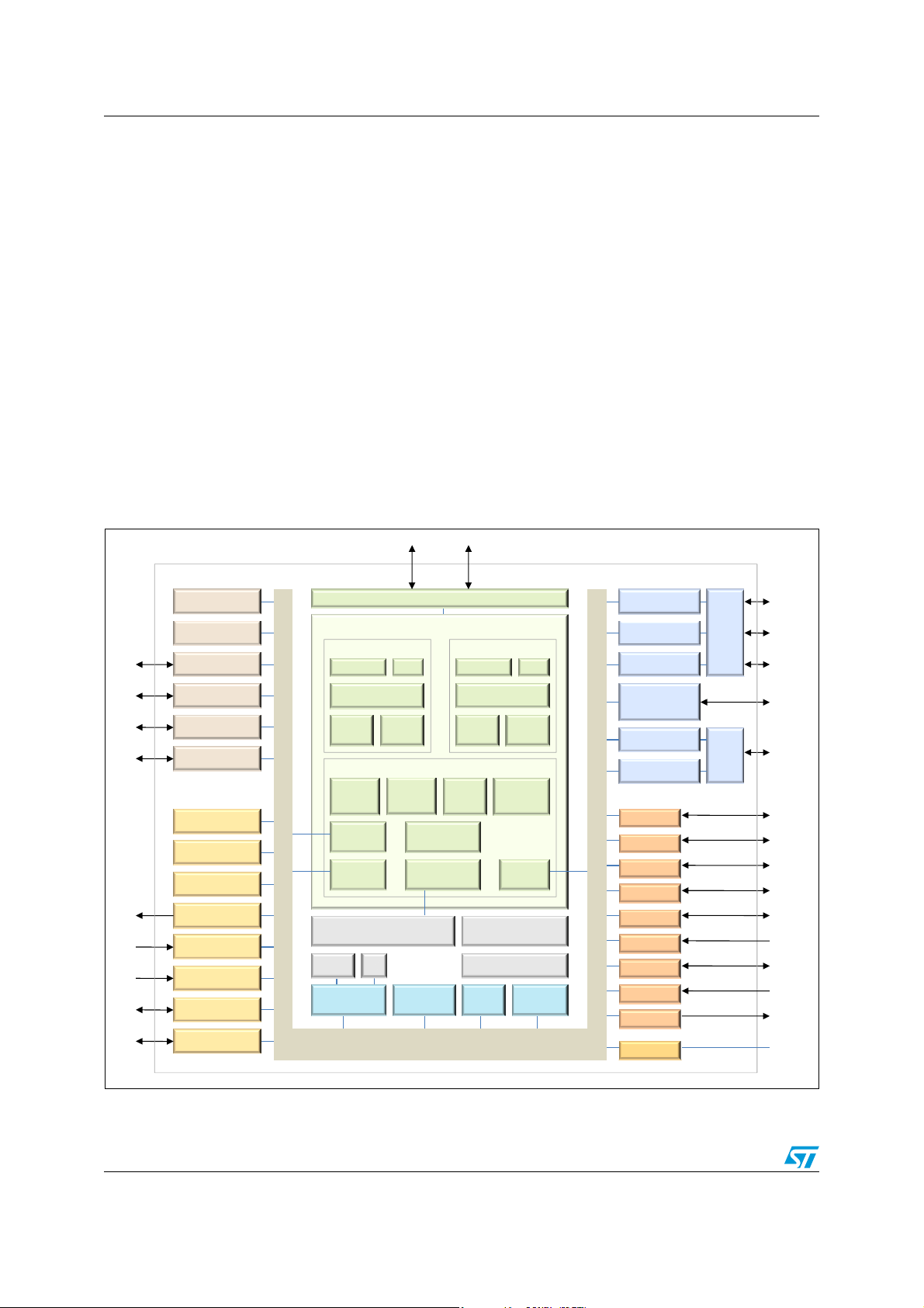
The architecture of SPEAr1340 is based on several internal components, communicating
through a multilayer interconnection matrix (BUSMATRIX). This switching structure enables
different data flows to be carried out concurrently, improving the overall platform efficiency.
In particular, high-performance master agents are directly interconnected with the DDR
memory controller in order to reduce access latency. The overall memory bandwidth
assigned to each master port can be programmed and optimized through an internal
weighted round-robin (WRR) arbitration scheme.
Figure 1. SPEAr1340 architectural block diagram
6/194 Doc ID 023063 Rev 2
Page 7

SPEAr1340 Device functions
2 Device functions
2.1 CPU subsystem
The CPU subsystem is based on the ARM Cortex A9 processor, and has a dual-core
configuration.
Main features:
Each core has the following features:
● ARM v7 CPU at 600 MHz
● 32 KB of L1 instruction CACHE with parity check
● 32 KB of L1 data CACHE with parity check
● Embedded FPU for single and double data precision scalar floating-point operations
● Memory management unit (MMU)
● ARM, Thumb2 and Thumb2-EE instruction set support
● Program Trace Macrocell (PTM) and CoreSight
● 32-bit timer with 8-bit prescaler
● Internal watchdog (working also as timer)
©
component for software debug
The dual core configuration is completed by a common set of components:
● Snoop control unit (SCU) to manage inter-process communication, cache-to-cache and
system memory transfer, cache coherency
● Generic interrupt control (GIC) unit configured to support 128 independent interrupt
sources with software configurable priority and routing between the two cores
● 64-bit global timer with 8-bit prescaler
● Accelerator coherence port (ACP)
● Parity support to detect runtime failures for other internal memories
● 512 KB of unified 8-way set associative L2 cache with support for ECC
● L2 Cache controller based on PL310 IP released by ARM
● Dual asynchronous 64-bit AMBA 3 AXI interface with possible filtering on the second
one to use a single port for DDR memory access
● JTAG interface and Trace port: debug and trace can be inhibited through OTP
Doc ID 023063 Rev 2 7/194
Page 8

Device functions SPEAr1340
2.2 Multilayer interconnect matrix (BUSMATRIX)
The multilayer interconnect matrix is the connectivity infrastructure that enables data
exchange between the various blocks of the device. The BUSMATRIX supports parallel
communications between master and slave components, and ensures the maximum level of
system throughput.
Main features:
● Hierarchical structure to meet the requirements of different system blocks and
peripherals:
– high performance low latency
– high performance medium latency
– medium performance medium/long latency
– slow peripherals and configurations
● Power awareness through the power down request/acknowledgement of the power
management module
● Single interrupt for outband signaling
2.3 Internal memories
SPEAr1340 integrates two embedded memories:
● 32 KB Boot ROM (BootROM)
● Static RAM areas (SRAM)
2.3.1 BootROM
BootROM refers to the on-chip 32 KB ROM as well as the booting firmware pre-stored in
such memory. The supported booting devices are:
● Serial NOR Flash
● Parallel NOR Flash
● NAND Flash
● USB OTG
● UART
● SD/MMC
The BootROM firmware selects the booting device after reset by reading the status of the
STRAP[3:0] pins.
2.3.2 Static RAMs (SRAM)
A part of these memory areas is used during the bootstrap phase by BootROM firmware.
After booting, all SRAM areas are fully available for general purpose applications.
Main features:
● 32 KB of system RAM (SYSRAM0, single port)
When all power islands are switched off, SYSRAM0 loses its data content.
● 4 KB of Always-on RAM (SYSRAM1, single port)
When all power islands are switched off, SYSRAM1 maintains its data content.
8/194 Doc ID 023063 Rev 2
Page 9

SPEAr1340 Device functions
2.4 Multiport DDR controller (MPMC)
MPMC is a high-performance multichannel memory controller able to support DDR2 and
DDR3 memory devices. The multiport architecture ensures that memory is shared efficiently
among different high-bandwidth client modules.
Main features:
● Supports both DDR3 and DDR2 devices; wide range of memory device cuts supported
up to 2 GB (Note: 1)
● Two chip selects supported
● Programmable memory data path size of full memory 32-bit data width or half memory
16-bit data width
● Clock frequencies from 100 MHz to 533 MHz supported
● 6 AXI interfaces with a data interface width of 64 bits. Each port is configured with a
thread ID of 4 bits
● Exclusive and locked accesses support
● Weighted round-robin arbitration scheme support to ensure high memory bandwidth
utilization
● DRAM command processing
● Register port with an AHB interface with a data interface width of 32 bits
● A programmable register interface to control memory device parameters and protocols
including auto pre-charge
● Full initialization of memory on memory controller reset
● Automatically maps user addresses to the DRAM memory in a contiguous block
addressing starts at user address 0 and ends at the highest available address
according to the size and number of DRAM devices present
● Fully pipelined command, read and write data interfaces to the memory controller
● Advanced bank look-ahead features for high memory throughput
Note: 1 When the 2GB address space is enabled, the ACP function is not available.
2.5 Serial NOR Flash controller (SMI)
The serial NOR Flash controller integrated in SPEAr1340 acts as an AHB slave interface
(32-, 16- or 8-bit) to SPI-compatible off-chip memories. SMI allows the CPU to use these
serial memories either as data storage or for code execution.
Main features:
● Supports a group of SPI-compatible Flash and EEPROM devices
● Acts always as an SPI master and up to 2 SPI slave memory devices are supported
(through as many chip select signals), with up to 16 MB address space each.
● The SMI clock signal (smi_clk_o) is generated by SMI (and inputs to all slaves) using a
clock provided by the AHB bus
● smi_clk_o can be controlled by a programmable 7-bit prescaler allowing 127 different
clock frequencies.
Doc ID 023063 Rev 2 9/194
Page 10

Device functions SPEAr1340
2.6 Flexible static memory controller (FSMC)
The flexible static memory controller enables to interface external parallel Flash memories
as well as static RAMs.
Main features:
● Support for parallel NAND Flash:
– 8-bit or 16-bit data bus
– 2 chip select signals
– no limitation on NAND capacity (number of pages)
– hardware ECC (error correction code) support, correcting up to 8 errors per page
(512 bytes wide)
– support for SLC (single-level cell) and MLC (multi-level cell) Flash devices, as far
as compatible with available ECC features
● Support for parallel NOR Flash:
– 8-bit or 16-bit data bus
– 26-bit address bus
– 2 chip select (CS) signals
– Maximum capacity is 64 MB for each CS, hence up to 128 MB with 2 external
Flash devices
● Support for asynchronous static RAMs (SRAMs):
– 8-bit or 16-bit data bus
– 26-bit address bus
– 2 chip select (CS) signals
– Maximum capacity is 64 MB for each CS, hence up to 128 MB with 2 external
SRAM devices
● Support for multiplexed NOR and SRAM
● Write FIFO: 16 words depth, each word is 32 bits wide
● Independent read/write timings and protocol, allowing matching the widest variety of
memories and timings
● Wait signal for timings handshake
10/194 Doc ID 023063 Rev 2
Page 11

SPEAr1340 Device functions
2.7 USB 2.0 Host controllers (UHC)
The SPEAr1340 device integrates 2 USB Host interfaces. Each interface provides a highspeed Host controller (EHCI standard) and a full-speed/low-speed controller (OHCI
standard). The UHC has 2 physical ports (2 separate instances) that are fully compliant with
the Universal Serial Bus specification (version 2.0), and provides an interface to the
industry-standard AHB bus.
Main features:
● A PHY interface implementing a USB 2.0 transceiver macro-cell interface plus (UTMI+)
fully compliant with UTMI+ specification (revision 1.0), to execute serialization and deserialization of transmissions over the USB line
● Either 30 MHz clock for 16-bit interface or 60 MHz for 8-bit interface supported by the
UTMI + PHY interface
● A USB 2.0 host controller (UHC) connected to the AHB bus that generates the
commands for the UTMI+PHY
● Complies with both the enhanced host controller interface (EHCI) specification (version
1.0) and the open host controller interface (OHCI) specification (version 1.0a)
● The UHC supports the 480 Mbps high-speed (HS) for USB 2.0 through an embedded
EHCI Host Controller, as well as the 12 Mbps full-speed (FS) and the 1.5 Mbps lowspeed (LS) for USB 1.1 through one integrated OHCI Host controller
● All clock synchronization is handled within the UHC
● An AHB slave for each controller (1 EHCI and 1 OHCI), acting as programming
interface to access to control and status registers
● An AHB master for each controller (1 EHCI and 1 OHCI) for data transfer to system
memory, supporting 8-, 16-, and 32-bit wide data transactions on the AHB bus
● 32-bit AHB bus addressing
2.8 USB 2.0 OTG port (UOC)
Main features:
● Complies with the On-The-Go supplement to the USB 2.0 specification (revision 1.3)
● Supports the Session Request Protocol (SRP)
● Supports the Host Negotiation Protocol (HNP)
● A PHY interface implementing the USB 2.0 transceiver macrocell interface (UTMI+
specification, revision 1.0 (Level 3)) to execute serialization and de-serialization of
transmissions over the USB line
● Unidirectional and bidirectional 16-bit UTMI data bus interfaces
● Support for the following speeds:
– High speed (HS): 480 Mbps
– Full speed (FS): 12 Mbps
– Low speed (LS): 1.5 Mbps (only in Host mode)
● Both of the DMA and slave-only modes are supported
Doc ID 023063 Rev 2 11/194
Page 12

Device functions SPEAr1340
2.9 Giga/Fast Ethernet port (GMAC)
The GMAC IP provides the capability to transmit and receive data over Ethernet.
Main features:
● Supports 10/100/1000 Mbps data transfer rates with the following PHY interfaces:
– IEEE 802.3-compliant GMII/MII interface (default) to communicate with an external
Gigabit/Fast Ethernet PHY
– RGMII interface to communicate with an external gigabit PHY
– RMII interface (specification version 1.2 from RMII consortium) to communicate
with an external Fast Ethernet PHY (for 10/100 Mbps operations only)
● Full-duplex operation:
– IEEE 802.3x flow control automatic transmission of zero-quanta pause frame on
flow control input de-assertion
– Optional forwarding of received pause control frames to the user application
● Half-duplex operation:
– CSMA/CD Protocol support
– Flow control using back-pressure support
– Frame bursting and frame extension in 1000 Mbps half-duplex operation
● Automatic CRC and pad generation controllable on a per-frame basis
● Provides options for automatic pad/CRC stripping on receive frames
● Supports a variety of flexible address filtering modes, such as:
– Up to 31 48-bit SA address comparison check with masks for each byte
– 64-bit hash filter for multicast and unicast (DA) addresses
– Option to pass all multicast addressed frames
– Promiscuous mode support to pass all frames without any filtering for network
monitoring
– Passes all incoming packets (per filter) with a status report
● Programmable frame length to support standard or jumbo Ethernet frames with up to
16 KB of size
● Programmable interframe gap (IFG) (40-96 bit times in steps of 8)
● Separate 32-bit status for transmit and receive packets
● IEEE 802.1Q VLAN tag detection for reception frames
● Self-managed DMA transfers with an internal DMA block
● Separate transmission, reception, and control interfaces to the application
– The host CPU uses a 32-bit AHB (AMBA 2.0) slave interface to access the GMAC
subsystem control and status registers (CSRs)
– The GMAC transfers data to system memory through a 32-bit AXI (AMBA 3.0)
master interface
● Support for network statistics with RMON/MIB counters (RFC2819/RFC2665)
● A module for detection of LAN remote wake-up frames and AMD magic packet frames:
power management module (PMT)
● A receive module for checksum off-load for received IPv4 and TCP packets
encapsulated by the Ethernet frame (Type 1)
● An enhanced receive module for checking IPv4 header checksum and TCP, UDP, or
ICMP checksum encapsulated in IPv4 or IPv6 datagrams (Type 2)
12/194 Doc ID 023063 Rev 2
Page 13

SPEAr1340 Device functions
● An enhanced module to calculate and insert IPv4 header checksum and TCP, UDP, or
ICMP checksum in frames transmitted in store-and-forward mode.
● A module to support Ethernet frame time stamping as described in IEEE 1588- 2002
and IEEE 1588-2008 (standard for precision networked clock synchronization). Sixtyfour-bit time stamps are given in the transmit or receive status of each frame.
● MDIO master interface for PHY device configuration and management: station
management agent (SMA), MDIO module
● Supports the standard IEEE P802.3az, version D2.0 for energy efficient Ethernet;
allows physical layers to operate in the low-power idle (LPI) mode
The MAC transaction level (MTL) block consists of two sets of FIFOs: a transmit FIFO
with programmable threshold capability, and a receive FIFO with a programmable threshold
(default of 64 bytes). The MTL block has the following features:
● 32-bit transaction layer block that provides a bridge between the application and the
GMAC
● Single-channel transmit and receive engines
● Synchronization for all clocks in the design (transmit, receive, and system clocks)
● Optimization for packet-oriented transfers with frame delimiters
● Four separate ports for system-side and GMAC side transmission and reception
● FIFO instantiation outside the top-level module to facilitate memory testing/instantiation
● 4 KB receive FIFO size on reception
● Supports receive status vectors insertion into the receive FIFO after the EOF transfer.
This enables multiple-frame storage in the receive FIFO without requiring another FIFO
to store those frames
● Configurable receive FIFO threshold (default fixed at 64 bytes) in cut-through or
threshold mode
● Provides an option to filter all error frames on reception and not forward them to the
application in store-and-forward mode.
● Provides an option to forward under-sized good frames
● Supports statistics by generating pulses for frames dropped or corrupted (due to
overflow) in the receive FIFO
● 2 KB FIFO size on transmission
● Store and forward mechanism for transmission to the GMAC
● Threshold control for transmit buffer management
● Automatic retransmission of collision frames for transmission
● Discards frames on late collision, excessive collisions, excessive deferral, and under-
run conditions
● Software control to flush TX FIFO
The DMA block exchanges data between the MTL block and host memory. The host can
use a set of registers (DMA CSR) to control the DMA operations. The DMA block supports
the following features:
● 32-bit data transfers
● Single-channel transmit and receive engines
● Fully synchronous design operating on a single system clock (except for CSR module,
when a separate CSR clock is configured)
● Optimization for packet-oriented DMA transfers with frame delimiters
Doc ID 023063 Rev 2 13/194
Page 14

Device functions SPEAr1340
● Byte-aligned addressing for data buffer support
● Dual-buffer (ring) or linked-list (chained) descriptor chaining
● Descriptor architecture that allows large blocks of data transfer with minimum CPU
intervention
● Comprehensive status reporting for normal operation and transfers with errors
● Individual programmable burst size for transmit and receive DMA engines for optimal
host bus utilization
● Programmable interrupt options for different operational conditions
● Complete per-frame transmit/receive interrupt control
● Round-robin or fixed-priority arbitration between receive and transmit engines
● Start/stop modes
● Separate ports for host CSR access and host data interface
The GMAC audio video (AV) enables transmission of time-sensitive traffic over bridged
local area networks (LANs). The GMAC AV has the following features:
● Compliant to IEEE 802.1-AS standard, version D6.0: specifies the protocol and
procedures used to ensure that the synchronization requirements are met for timesensitive applications
● Compliant to IEEE 802.1-Qav standard, version D6.0: allows the bridges to provide
time-sensitive and loss-sensitive real-time audio video data transmission (AV traffic). It
specifies the priority regeneration and controlled bandwidth queue draining algorithms
that are used in bridges and AV traffic sources
● Supports one additional channel (channel 1) on the transmit and receive paths for AV
traffic in 100 Mbps and 1000 Mbps modes. The channel 0 is available by default and
carries the legacy best-effort Ethernet traffic on the transmit side.
● Supports IEEE 802.1-Qav specified credit-based shaper (CBS) algorithm for the
additional transmit channels
● Provides separate DMA, TxFIFO, and RxFIFO MTL for the additional channel (to avoid
“head of line blocking” issues); the system-side interface remains the same.
The GMAC has the following additional features for monitoring, testing, and debugging:
● Supports internal loopback on the GMII/MII for debugging
● Provides DMA states (Tx and Rx) as status bits
● Provides debug status register that gives status of FSMs in transmit and receive data-
paths and FIFO fill-levels
● Application abort status bits
● MMC (RMON) module in the GMAC core
● Current Tx/Rx buffer pointer as status registers
● Current Tx/Rx descriptor pointer as status registers
● Statistical counters that help in calculating the bandwidth served by each transmit
channel when AV support is enabled
14/194 Doc ID 023063 Rev 2
Page 15

SPEAr1340 Device functions
2.10 PCI Express controller (PCIe)
The PCI Express core incorporates a dual-mode (DM) core which can implement a PCIe
interface for a PCIe Root Complex (RC) or Endpoint (EP). The dual-mode core can operate
in EP or RC port modes, depending on value written in a register during PCIe configuration.
PCIe is compliant with the PCI Express Base 2.0 specification, but it is also compliant with
the PCIe 1.1 specification.
The core features a proprietary user-configurable and high-performance application
interface for generating and receiving PCIe traffic. It is available with standard AMBA 3 AXI
interfaces.
Typical applications for a PCI Express device built with the DM core include:
● Motherboard components for desktop and mobile computers
● Graphics devices
● Add-in cards for desktop and mobile computers
● Components and add-in cards in server applications
● Embedded applications
● Data communications equipment
● Telecommunications equipment
● Storage devices
● Wireless devices
● Other applications
The DM core in EP mode supports PCI Express Legacy Endpoint devices. However, the
application must ensure that the device obeys the Legacy Endpoint device rules defined in
the PCI Express Base 2.0 specification.
Note: The core is not intended for use in a root complex integrated endpoint.
Main features (common to both EP and RC mode of the DM cores):
● Support for all non-optional features and some optional features defined in the PCI
Express Base 2.0 specification.
● Ultra low transmit and receive latency
● Support a max payload size of 256 bytes
● 4 KB maximum request size
● Very high accessible bandwidth
● Support for both Gen1 (at 125 MHz) and Gen2 (at 250 MHz) operation
● 2.5 Gbps (Gen1) or 5.0 Gbps (gen2) Lane (x1)
● Automatic lane reversal as specified in the PCI Express 2.0 specification (transmit and
receive)
● Polarity inversion on receive
● Multiple virtual channels (VCs) (maximum of 2)
● Multiple traffic classes (TCs)
● ECRC generation and checking
● PCI Express beacon and wake-up mechanism
Doc ID 023063 Rev 2 15/194
Page 16

Device functions SPEAr1340
● PCI power management
● PCI Express active state power management (ASPM)
● PCI Express advanced error reporting
● Vital product data (VPD)
● PCIe messages for both transmit and receive.
● External priority arbitration (in addition to the internally implemented transmit
arbitration)
● Expansion ROM support
Additional features specific to RC mode
● Type 1 configuration space
● Application-initiated Lane reversal for situations where the core does not detect Lane 0
(for example, an x4 core connected to an x8 device that has its Lanes reversed)
Additional features specific to EP mode
● Completion time-out ranges
● Type 0 configuration space
● MSI interrupt capability
2.11 Serial ATA controller (SATA)
The SATA AHCI Core implements the serial advanced technology attachment (SATA)
storage interface for physical storage devices.
Main features:
● SATA 3.0 Gb/s Gen II
● eSATA (external analog logic also needs to support eSATA)
● Compliant with the following specifications:
– Serial ATA 3.0 (except FIS-based switching)
– AHCI Revision 1.3 (except FIS-based switching)
– AMBA 3 AXI interfaces
● User-defined PHY status and control ports
● RX data buffer for recovered clock systems
● Data alignment circuitry when RX data buffer is also included
● OOB signaling detection and generation
● 8b/10b encoding/decoding
● Asynchronous signal recovery, including retry polling
● Digital support of device hot-plugging
● Power management features including automatic partial-to-slumber transition
● BIST loopback modes
● Single SATA device
● Internal DMA engine per port
● Hardware-assisted native command queuing for up to 32 entries
16/194 Doc ID 023063 Rev 2
Page 17

SPEAr1340 Device functions
● Port Multiplier with command-based switching
● Disabling RX and TX Data clocks during power down modes
● Integrated SATA link layer and transport layer logic
● Supports PIO, first party and legacy DMA modes
● Supports legacy command queuing
● Supports ATA and ATAPI master-only emulation mode (for instance, register and
command compatible with these standards)
● Power-down mode
● Data scrambling
● CRC computation
● Automatic data flow control
● Far end loop-back re-timed
2.12 SATA/PCIe physical interface (MiPHY)
The MiPHY macrocell implements the lower (physical) layer protocols providing data
transmission and reception over a dual differential pair cable. The TX (transmit) and RX
(receive) serial channels operate plesiochronously (NRZ). The macrocell can be used in
Host or Device applications.
Main features:
● Serial transceiver (PHYsical layer) serializer and deserializer
● Direct support for 1.5/ 3.0 and 1.25/ 2.5/ 5.0 Gbit/s bit rates
● 20-bit parallel interface
● Comma detect to provide word alignment of incoming serial stream
● SSC modulation
● Integrated impedance adaptation to transmission line characteristics
● Out-of-band (OOB) signaling
● Supported 1.2 V and 2.5 V power supply
● High-performance PLL (input reference 100 MHz for PCIe and 100 or 25 MHz for
SATA)
● Programmable TX buffer pre-emphasis, slew-rate and amplitude
● Dedicated TX buffer regulator for:
– Transmit buffer noise immunity
– Buffer level stability
Doc ID 023063 Rev 2 17/194
Page 18

Device functions SPEAr1340
2.13 Memory card interfaces (MCIF)
MCIF is a hardware IP that interfaces with the most common memory cards on the market:
● SD/SDIO 2.0
● SDHC
● CF/CF+ Rev 4.1
● MMC 4.2/4.3
● xD
The device interface multiplexes different memory cards on the same IOs; only one memory
card is accessible at a given time. At the board level, discrete elements are required to
handle host-swap management.
Main features:
SD/SDIO/MMC controller
● Compliant with:
– SD Host controller standard specification version 2.0
– SDIO card specification version 2.0
– SD memory card specification draft version 2.0
– SD memory card security specification version 1.01
– MMC specification version 3.31, 4.2 and 4.3
– AMBA specification AHB (version 2.0)
● Data transfer with the system core through:
– PIO mode on the Host AHB slave interface
– DMA mode on the Host AHB master interface
● Host clock rate variable from 0 to 50 MHz
● Maximum data rate achievable:
– 200 Mbps (sd4 bit mode)
– 400 Mbps (mmc8 bit mode)
● Data transfer:
– SD mode: 1 bit, 4 bit, and SPI mode
– MMC mode: 1 bit, 4 bit, 8 bit, and SPI mode
● Cyclic redundancy check for commands (CRC7) and for data integrity (CRC16)
● Variable length data transfer
● Read wait control and suspend/resume operations supported
● Works with IO cards, read-only cards and read/write cards
● Supports MMC Plus and MMC Mobile
● Error correction code support for MMC 4.3 cards
● Card detection (insertion/removal)
● Card password protection
● Two 4K FIFO to aid data transfer between the CPU and the controller
● FIFO overrun and underrun handled by stopping the SD clock
18/194 Doc ID 023063 Rev 2
Page 19

SPEAr1340 Device functions
CF/CF+ Host controller
● CF Specification Revision 4.1 compliance (True IDE Mode only)
● Multiword DMA to transfer data between the host and the CF/+ device
● Ultra DMA mode for accessing the CF/+ card using the 16-bit data path
● PIO timing mode0 through mode6
● Multiword DMA timing mode0 through mode4
● Ultra DMA timing mode0 through mode6
● Data transfers up to 256 (512 byte) blocks
● Variable-length data transfer in multiword DMA and Ultra DMA modes
● Interrupt-driven data transfers in PIO mode
xD Host controller (Xtreme Digital)
● Comfortable erase mechanism
● Programmable access timing
● Read, write, erase, read device ID, status and reset commands
● ECC generation and checking
● Multiblock programming and multiblock erase
● 1 Gbit, 2 Gbit support
2.14 UART ports
The SPEAr1340 device integrates 2 instances of an asynchronous serial port (UART) digital
block, identified as UART0 and UART1.
Asynchronous serial ports are responsible for performing the main tasks in serial
communications with computers. The device converts incoming parallel information into
serial data and incoming serial information into parallel data that can be sent on a
communication line connected to an external peripheral device.
The SPEAr1340 embedded MPU provides two independent UART controllers. One of the
typical uses of UART is connecting the SPEAr-based platforms to debugging consoles, the
communication with modems and the interfacing of Bluetooth, DECT or ZigBee chipsets.
The UART features inside SPEAr1340 offer similar functionality to the industry-standard
16C650 UART device.
UART ports usually do not directly generate or receive the external signals used between
different items of equipment. External interface devices are used to convert the logic level
signals of the UART to and from the external signaling levels. External signals may be of
many different forms, such as RS-232, infrared and wireless radio. In particular, the UART
interfaces inside SPEAr1340 directly support (by software selection) the IrDA-compliant
Serial InfraRed (SIR) protocol.
The UART supports standard asynchronous communication bits (start, stop, and parity),
which
are added prior to transmission and removed on reception.
Doc ID 023063 Rev 2 19/194
Page 20

Device functions SPEAr1340
Main features:
UART0 and UART1:
● Support baud rate up to UARTCLK/16
● Programmable baud rate generation (integer and fractional parts)
● Support three options on the UARTCLK clock frequency:
– 48 MHz: maximum baud rate of 3 Mbps (48/16)
– 24 MHz: maximum baud rate of 1.5 Mbps (24/16)
– Programmable by software: up to 125 MHz with a maximum baud rate of 7.81
Mbps (125/16).
● Separate 16x8 transmit and 16x12 receive first-in, first-out memory buffers (FIFOs)
● Programmable FIFO disabling for 1-byte depth
● FIFO trigger levels selectable between 1/8, 1/4, 1/2, 3/4 and 7/8
● Independent masking of transmit FIFO, receive FIFO, receive time-out, and error
condition interrupts
● Support for direct memory access (DMA)
● False start bit detection
● Line break generation and detection
● Programmable usage of IrDA SIR encoder/decoder:
IrDA SIR ENDEC block provides:
– Support of IrDA SIR ENDEC functions for data rates up to 115.2 Kbits/second
half-duplex
– Support of normal 3/16 and low-power bit durations
– Programmable internal clock generator enabling division of reference clock by 1 to
256 for low-power mode bit duration
● Fully-programmable serial interface characteristics:
– data can be 5, 6, 7, or 8 bits
– even, odd, stick, or no-parity bit generation and detection
– 1 or 2 stop bit generation
UART0 only:
● Programmable hardware flow control which uses the CTS input and the RTS output to
automatically control the serial data flow
● Support modem status which uses:
– Input signals: Clear To Send (CTS), Data Carrier Detect (DCD), Data Set Ready
(DSR), and Ring Indicator (RI)
– Output modem control lines: Request To Send (RTS), and Data Terminal Ready
(DTR)
● Independent masking of modem status
20/194 Doc ID 023063 Rev 2
Page 21

SPEAr1340 Device functions
2.15 I2C bus controllers (I2C)
The SPEAr1340 device integrates 2 instances of an I2C controller, identified as I2C0 and
I2C1, which can be used to connect to the I2C bus peripheral.
Main features:
● Compliant to the I2C-bus specification from Philips
● Three different operating modes:
– Standard-speed mode (data rates up to 100 Kb/s)
– Fast-speed mode (data rates up to 400 Kb/s)
– High-speed mode
● Clock synchronization
● Master or slave I2C operation mode
● Multimaster operation mode (bus arbitration)
● Support for direct memory access (DMA)
● 7-bit or 10-bit addressing
● 7-bit or 10-bit combined format transfers
● Slave bulk transfer mode
● Ignores CBUS addresses (an older ancestor of I2C that used to share the I2C bus)
● Buffer transmission and reception
● Interrupt or polled-mode operation
● Handles bit and byte waiting at all bus speeds
● Digital filter for the received SDA and SCL lines
2.16 Synchronous serial port (SSP)
The synchronous serial port block includes a master or slave interface to enable
synchronous serial communication with slave or master peripherals.
Main features:
● Master or slave operation
● Programmable clock bit rate and prescaler
● Separate transmit and receive first-in, first-out memory buffers, 16-bit wide, 8 locations
deep
● Programmable choice of interface operation, SPI, Microwire, or TI synchronous serial
● Programmable data frame size from 4 to 16 bits
● Independent masking of transmit FIFO, receive FIFO, and receive overrun interrupts
● Internal loopback test mode available
● Support for direct memory access (DMA)
Doc ID 023063 Rev 2 21/194
Page 22

Device functions SPEAr1340
2.17 A/D converter (ADC)
SPEAr1340 integrates an analog-to-digital converter.
Main features:
● Successive approximation A/D conversion
● 10-bit resolution for the analog cell which can be extended up to 12 bits with embedded
oversampling techniques performed by the controller
● 1 MSPS
● 8 analog input channels (0 – 2.5 V)
● INL ± 1 LSB
● DNL ± 1 LSB
● Programmable conversion speed – minimum conversion time 1 µs
● Support for resistive touchscreen
2.18 HDMI CEC interfaces (CEC)
The SPEAr1340 device integrates 2 instances of a Consumer Electronics Control (CEC)
digital block, identified as CEC0 and CEC1.
CEC is an asynchronous transfer mode adaptation layer (AAL) protocol that provides highlevel control functions among the various audiovisual products in a user’s environment. CEC
operates at low speeds, with minimal processing and memory overhead.
Main features:
● AMBA 2.0 compatible
● One touch play: Play a device and make it the active source with the press of a button
● System standby: Set all devices to standby with the press of a button
● Preset transfer: Auto-configures device presets to match those of the TV
● One-touch record: Enables one-button recording
● Timer programming: Any device can program a recording device’s timer
● System information: Devices can auto-configure their language and country settings
● Deck control: A device can control and interrogate a playback device
● Tuner control: A device can control the tuner of another device
● Vendor specific commands: Enables the use of vendor-defined commands
● On-screen display (OSD): A device can display text on the TV screen
● Device menu control: A device can control the menu of another device
● Routing control: Enables CEC switch control, to stream a new source device
● Remote control pass through: Enables the passing on of remote control commands to
other devices
● Device OSD name transfer: System devices can request the preferred object-based
storage device (OSD) name of other system devices
22/194 Doc ID 023063 Rev 2
Page 23

SPEAr1340 Device functions
2.19 General purpose I/O (GPIO/XGPIO)
SPEAr1340 handles generic input/outputs in 3 ways. First, the device integrates 2 instances
of a general purpose I/O (GPIO) digital block, identified as GPIOA and GPIOB. Second, an
extended GPIO (XGPIO) feature is provided. Finally, it is possible to use the KBD controller
in GPIO mode (this feature is documented in
The GPIO block provides 16 programmable inputs or outputs (8 for GPIOA and 8 for
GPIOB). Each input/output can be controlled by software.
GPIO main features:
● 16 individually programmable input/output pins (by default input at reset)
● An APB slave acting as control interface in software mode
● Programmable interrupt generation capability on any number of pins
● Bit masking in both read and writes operation through address lines
The XGPIOs are individually programmable input/output pins (by default output) that can be
controlled through an AHB slave interface.
XGPIO main features:
● 234 individually programmable input/output pins: XGPIO0 to XGPIO7, and XGPIO24 to
XGPIO249 (by default output). There is just an exception for the bit XGPIO169 which is
always an output.
● Programmable interrupt (rise or fall edge sensitive) generation on any number of pins
● An AHB slave interface as control
Section 2.28: Keyboard controller (KBD)).
Doc ID 023063 Rev 2 23/194
Page 24

Device functions SPEAr1340
2.20 LCD display controller (CLCD)
The TFT LCD controller provides all the necessary control signals to interface directly to a
variety of TFT LCD panels.
Main features:
● Wide range of programmable LCD panel resolutions
● Support for 1 port TFT LCD panel interfaces:
– 18-bit digital (6-bit/color)
– 24-bit digital (8-bit/color) CMOS
● Support for 2 Port TFT LCD panel interfaces (2
signals)
● Support for up to 2 overlay windows.
● Programmable frame buffer bits-per-pixel (bpp) color depths:
– 1, 2, 4, 8 bpp mapped through the color palette to 18-bit LCD pixel
– up to 18 bpp directly drive 18-bit LCD pixel
– 24 bpp directly drive 24-bit LCD pixel
● Color Palette RAM to reduce Frame Buffer memory storage requirements bandwidth
● Programmable output format support:
– RGB 6:6:6 or 5:6:5 or 5:5:5 on 18-bit digital interface
– RGB 8:8:8 on 24-bit digital interface
● Programmable horizontal timing parameters:
– horizontal front porch, back porch, sync width, pixels-per-line
– horizontal sync polarity
● Programmable vertical timing parameters:
– vertical front porch, back porch, sync width, lines-per-panel
– vertical sync polarity
● Programmable pixel clock frequency up to 148MHz (1080p resolution)
● Programmable data enable timing signal:
– derived from horizontal and vertical timing parameters
– display enable polarity
● Power up and down sequencing support
● Programmable endianness
● Pulse width modulation for LCD panel LED backlight brightness control
nd
port available by programmable
24/194 Doc ID 023063 Rev 2
Page 25

SPEAr1340 Device functions
2.21 Graphics processing unit (GPU)
The Mali GPU is a hardware accelerator for 2D and 3D graphics systems that forms the
basis of a high performance graphics processing solution. When implemented as part of a
system-on-chip (SoC) device, the GPU forms an integral part of the graphics solution. The
GPU comprises the following:
● an ARM
● a MaliGP2 geometry processor
● a memory management unit (MMU)
● associated software (programmed using OpenVG or OpenGL base layers)
Main features (pixel processor):
● Programmable fragment shader
● Access to framebuffer from fragment shaders
● Alpha blending
● Arbitrary memory reads and writes
● Complete non-power-of-2 texture support
● Cube mapping
● Dynamic recursion
● Fast dynamic branching
● Fast trigonometric functions, including arctangent
● Full floating-point arithmetic
● Framebuffer blend with destination Alpha
● High dynamic range (HDR) textures and framebuffers
● Indexable texture samplers
● Line, quad, triangle, and point sprites
● Multiple render targets
● No limit on program length
● Perspective anisotropic filtering (AF)
● Perspective correct texturing
● Point sampling, bilinear, and trilinear filtering
● Programmable mipmap level-of-detail biasing and replacement
● Register indirect jumps
● Stencil buffering, 8-bit
● Two-sided stencil
● Unlimited dependent texture reads
● Virtualized texture samplers
● 4-level hierarchical Z and stencil operations
● 4 times and 16 times full scene anti-aliasing (FSAA)
● 4-bit per texel texture compression.
®
Mali™200 pixel processor
Geometry processor
● Programmable vertex shader
● Autonomous operation tile list generation
● Flexible input and output formats
● Indexed and non-indexed geometry input
● Primitive constructions with points, lines, triangles and quads.
Doc ID 023063 Rev 2 25/194
Page 26

Device functions SPEAr1340
Software
● Compatibility with the following graphics standards:
– OpenGL ES 2.0
– OpenGL ES 1.1
– OpenVG 1.0
The geometry processor must be programmed using OpenVG or Open GL base layers.
2.22 Video decoder (VDEC)
Main features:
● All algorithms in hardware - minimal CPU load
● Minimal power consumption - functional level clock gating and synthesis time clock
gating (> 90% of registers under gating)
Supported video codecs:
● H.264 profile and level
– Baseline, main and high profiles
– Decoding up to 1080p/30fps
– Scalable video coding (SVC):
– Baseline and high profiles (base layer only)
● MPEG-4 visual profile and level
– Simple and advanced simple profiles, levels 0 –5
●
H.263 profile and level
– Profile 0, levels 10 –70 (image size up to 720x576)
● Sorenson Spark
● WMV9 / VC-1
– Simple, main and advanced profiles, levels 0 -3
● MPEG-1&2 main profile
– Low, medium and high levels
● RealVideo8/9/10
● DivX®3/4/5/6 support
– Home theater profile qualification
● VP6, VP7 versions 0-3
● VP8 version 2 (WebM)
● AVS Jizhun Profile
● JPEG, all common sampling formats
– Baseline interleaved
(1)
(2)
1. Achievable resolution and frame rate depending on specific stream content and system load.
2. Global motion compensation (GMC) is not supported.
26/194 Doc ID 023063 Rev 2
Page 27

SPEAr1340 Device functions
Supported post-processing features:
● Input image source
– Internal source (combined mode): G1decoder
– External source (standalone mode): for example, a software decoder or camera
interface
● Input image size
– Combined mode: 48 x 48 to 8176 x 8176 (66.8 Mpixels)
– Standalone mode: width from 48 to 8176, height from 48 to 8176 (maximum size
limited to 16.7 Mpixels)
● Output image size
– 16 x 16 to 1920 x 1088
● Image scaling
– Bicubic polynomial interpolation for upscaling
– Proprietary averaging filter for downscaling
– Arbitrary, non-integer scaling ratio separately for both dimensions
● YCbCr to RGB color conversion
– BT.601-5 compliant
– BT.709 compliant
– User definable conversion coefficient
● Dithering
– 2x2 ordered spatial dithering for 4-, 5- and 6-bit RGB channel precision
● Alpha blending
– Output image can be alpha blended with two rectangular areas
● Deinterlacing
– Conditional spatial deinterlace filtering; supports only YCbCr 4:2:0 input format
● linear RGB image contrast, brightness and color saturation adjustment
● Deblocking filter for MPEG-4 simple profile /H.263 / Sorenson
– Using a modified H.264 in-loop filter as a postprocessing filter; filtering has to be
performed in combined mode.
● Image cropping / digital zoom
– User definable start position, height and width
– Usable only for JPEG or stand-alone mode
● Output image masking
● Image rotation
– Rotation 90, 180 or 270 degrees
– Horizontal/vertical flip
Doc ID 023063 Rev 2 27/194
Page 28

Device functions SPEAr1340
2.23 Video encoder (VENC)
A multiformat video encoder is integrated in SPEAr1340 with 64-bit AXI master and 32-bit
AHB slave interfaces. It supports H.264 high profile video resolution up to 1080p and JPEG
still picture up to 64
Main features:
● H.264 profile and level
– Baseline, main and high profiles, levels 1- 4.0
● JPEG profile and level
– Baseline (DCT sequential)
● Video stabilization
● I and P slices support
● CAVLC baseline and CABAC main profile
● Error resilience
– Constrained intra prediction
– Slices, multiple of macro blocks rows
● Maximum motion vector length
– Vertical ±14 pixels
– Horizontal ±30pixels
● 12 intra prediction modes
● Motion vector pixel accuracy
– 720p resolution ¼ pixels
– 1080p resolution ½ pixels
● Macroblock and sub-macroblock partitions: 16x16, 8x16, 16x8, 8x8, 4x8, 8x4,4x4
● Transforms 4x4 baseline, main and high profiles
● 1 reference frame support
● Maximum 1 slice group support
● Input data formats
– Planar YCbCr 4:2:0, semiplanar YCbCr 4:2:0, interleaved YCbCr 4:2:2
● Output data formats
– H.264 (Byte and NAL unit stream)
– JPEG( JFIF file format 1.02 and non progressive JPEG)
● Supported image size
– H.264: 96x96 to1920x1020
– JPEG: 96x96 to 8192x8192
– Step size 4 pixels
● Pre-processing features
– YCbCr 4:2:2 to YCbCr 4:2:0 color space conversion for all YCbCr input formats
– Cropping from 8192 x 8192 to any supported encoding size
– Rotation of 90 or 270 degrees
Mpixel.
28/194 Doc ID 023063 Rev 2
Page 29

SPEAr1340 Device functions
2.24 Camera input interfaces (CAM)
The SPEAr1340 device integrates 4 instances of a camera input (CAM) digital block,
identified as CAM1, CAM2, CAM3, CAM4.
Each CAM interface enables SPEAr1340 to interface with an external image sensor. An
incoming image is stored in CAMIF memory per a programmed mode, and then transferred
to external memory using system direct memory access.
Main features:
● AMBA 2.0 compatible
● Slave interface with connection to external system DMA
● 8-bit parallel data interface
● YCbCr4:2:2, RGB888 packed, RGB888 un-packed, RGB565, JPEG mode
● Video mode with all running frame
● Compliant with ITU-R BT.601 (External synchronization) as well as ITU-R BT.656
(embedded synchronization)
● Image cropping
● Programmable polarity of pixel clock and external synchronization signals (HSYNCH,
VSYNCH)
Note: For 1080p 30 Hz video maximum pixel clock frequency for CAM required is
(2x2200x1125x30)=148.5
MHz.
2.25 Video input parallel port (VIP)
The video input parallel port is used to interface with some external image sensors.
Incoming images are stored inside its internal FIFO as per some programmed mode and
then transferred to the external memory through the master interface.
Main features:
● Supports HDMI, DVI, DP and CVBS
● Supports output format RGB along with HSYNC, VSYNC and pixel clock
● Clock polarity configuration provided (Positive edge/Negative edge)
● HSYNC and VSYNC polarity configurable
● Handling of data enable signal
● Dual-port display in DVI mode for 16 bpp and 24 bpp supported
● Input bit width 16 bpp, 24 bpp and 32 bpp supported
● Only unpacked data format supported
Doc ID 023063 Rev 2 29/194
Page 30

Device functions SPEAr1340
2.26 I2S digital audio ports (I2S)
The I2S controller is a highly configurable IP for use in audio applications. It provides a
simple interface to standard audio components.
Main features:
● Compliant to Philips I2S serial bus specifications
● I2S master for output operations and I2S slave for input operations
● Configurable number of stereo channels (up to 4) for both transmitter and receiver
● Supports up to 7.1 audio Tx and Rx
● Supports 12-/16-/20-/24-/32-bit audio data interface
● Fully synchronous design with serial clock and system clock
● Interrupt support for reporting FIFO and other conditions
● Programmable FIFO thresholds
● Supports data exchange to the system memory through DMA interface
● Software controlled block resets and enables
● Software controlled FIFO flush
2.27 S/PDIF digital audio port
The S/PDIF audio interface detects bi-phase encoded S/PDIF signals, and plays PCM audio
data or audio encoded bit streams stored in memory in the S/PDIF format.
Main features:
Input
● Fully compliant with IEC-60958 for audio data
● Supports typical audio sampling frequencies, such as 32, 44.1, 48, 96, and 192 kHz.
● Programmable DMA trigger threshold
● VUCP storage can optionally be disabled
● Audio data can be stored in bit lengths of 16 to 24 bits
Output
● Compliant with IEC-60958 for audio data and IEC-61937 for compressed audio data
● Supports typical audio sampling frequencies such as 32, 44.1, 48, 96, and 192 kHz
● Supports one-bit audio mode (HDMI)
● Supports DTS-HD mode
● Programmable system DMA trigger limit
● Programmable VUCP insertion
● Supports 16/0 or 16/16 audio data format in memory
2.28 Keyboard controller (KBD)
The GPIO keyboard controller integrated in SPEAr1340 offers a 3-mode input and output
port. It provides an12-bit GPIO, or 6x6 keyboard, or 2x2 keyboard plus 8-bit GPIO, and
offers an interface to the industry standard APB bus.
30/194 Doc ID 023063 Rev 2
Page 31

SPEAr1340 Device functions
Main features:
● AMBA APB interface
● GPIO or keyboard functionality with selection of any one of the two keyboard matrices:
– 12-bit general purpose parallel port (GPIO) with input or output single pin
programmability
– 36 (6x6) keys keyboard
– 4 (2x2) key keyboard plus 8-bit GPIO with input or output single pin
programmability
2.29 Cryptographic co-processor (C3)
C3 is a multipurpose, instruction driven, programmable DMA-based co-processor. It is
configured to accelerate cryptographic and network security functions.
Main features:
● AMBA AHB 2.0 master and slave interfaces
● Scatter and gather DMA engine (implemented only by MPCM channel)
● Instruction dispatchers
– ID0 and ID1 available
– ID2 and ID3 empty
● Internal RAM: 4Kx32
● Coupling/Chaining: 2 paths
The hardware accelerator crypto algorithms available in SPEAr1340 have the following
channels supported by mentioned operations:
● Channel 0: Move channel
– Supported operations: copy, AND, OR, XOR
– Chained mode: either master or slave
– Cascaded mode: both master and slave
– Input FIFO: 8x32 bits
– Output FIFO: 8x32 bits
● Channel 2: MPCM for the advanced encryption standard (AES)
– Supported algorithms: AES (128-, 192-, 256-bit keys, ECB and CBC
encryption/decryption, with programmable operation modes to support almost all
possible modes, including Counter and XTS mode)
– Memory for modes of operation: 512 words of 62 bits each
– Input FIFO: 16x32 bits
Doc ID 023063 Rev 2 31/194
Page 32

Device functions SPEAr1340
– Output FIFO: 16x32 bits
– Read scatter/gather list: 4x32 bits
– Write scatter/gather list: 4x32 bits
● Channel 3: Unified hash with HMAC
– Supported algorithms: HMAC MD5 (hash with 128-bit digest), HMAC SHA1 (hash
with 160-bit digest) and HMAC SHA2 (SHA256 and SHA224 with 256- and 224-bit
digest respectively)
– Input FIFO: 16x32 bits
– Output FIFO: 8x32 bits
● Channel 4: Unified hash 2 with HMAC
– Supported algorithms: HMAC SHA384 (hash with 384-bit digest) and HMAC
SHA512 (hash with 512-bit digest)
– Input FIFO: 16x32 bits
– Output FIFO: 8x32 bits
● Channel 5: Public key accelerator (PKA) v6
– Supported algorithms: modular exponentiation for RSA and Diffie-Hellman (up to
2048 bits), scalar multiplication of elliptic curve points over prime fields for ECC
(up to 384 bits) and Montgomery’s parameter for finite field operations
– Input FIFO: 8x32 bits
– Output FIFO: 8x32 bits
● Channel 6: Random number generator (RNG)
– Generates a sequence of true random numbers, based on a contiguous analog
oscillator; the sequence has a success ratio of more than 85 % for 20.000 bits,
according to FIPS 140-1 tests
– Monitors the entropy of the generated sequence
– Input FIFO: 2x32 bits
– Output FIFO: 4x32 bits
2.30 Real-time clock (RTC)
The RTC is a block that keeps track of the real time of day. It also functions as an alarm and
a calendar. The time is displayed in 24-hour format, and time/calendar values are stored in
binary-coded decimal format.
The time of day, alarm and calendar, status and control registers can all be accessed via a
standard 32 APB bus. All read/write operations last 2 cycles.
RTC provides a self-isolation mode that is activated during power down. This allows RTC to
continue its operation (except for the alarm interrupt feature that is not preserved) if power is
not supplied to the rest of the circuit. This feature is realized by supplying separate power
and clock connections.
A set of 16 general purpose registers (GP-Reg) are provided which can be used to save
data during the power down state. GP-Reg-set runs on 32
RTC battery. Each register is of 32 bits and addressed mapped on the 32-bit APB bus. A bit
in status register reflects the status of any pending write to GP-Reg-set. This means that
write operation to the GP-Reg-set should be sequential, so you should wait for this pending
status bit to be cleared before writing again to GP-Reg-set.
32/194 Doc ID 023063 Rev 2
K oscillator clock and powered by
Page 33

SPEAr1340 Device functions
Main features:
● Works on dedicated 32768 Hz external clock and power supply
● 9999- year calendar
● Leap years support
● Programmable alarm interrupt
● Power management and self-isolation
● Prescaler and timer registers bypass for TEST
● Time and date update monitors
● 16 general purpose registers which can be used to save data during power down state
2.31 DMA controllers (DMAC)
The SPEAr1340 device integrates 2 instances of a DMA controller (DMAC) digital block,
identified as DMAC0 and DMAC .
The DMAC is an AHB-central DMA controller core that transfers data from a source
peripheral to a destination peripheral over two AHB buses. A wrapper is designed to
instantiate 2 DMAC cores (each with 2 AHB master interfaces), 2 ICMs (which arbitrate the
same master interface of each DMAC) and a MUX (which manages multiple peripheral
handshaking interfaces).
Main features:
● AMBA 2.0-compliant
● AHB slave interface – used to program the DMAC
● 8 channels, one per source and destination pair
● Unidirectional channels – data transfers in one direction only
● Programmable channel priority
● 2 independent AHB master interfaces
● Data bus width configured to 64 bits for each AHB master interface
● Configurable endianness for master interfaces
● Support for memory-to-memory, memory-to-peripheral, peripheral-to-memory, and
peripheral-to-peripheral DMA transfers
● Component ID parameters for configurable software driver support
● Programmable source and destination addresses (on AHB bus)
● Address increment, decrement or no change
● Multiblock transfers achieved through linked lists (block chaining)
● Independent source and destination selection of multiblock transfer type
● Scatter/Gather
Doc ID 023063 Rev 2 33/194
Page 34

Device functions SPEAr1340
● Single FIFO per channel for source and destination
● FIFO depth configured to 16 bytes for the first 4 channels and to 128 bytes for the last 4
channels
● D flip-flop-based FIFO
● Automatic data packing or unpacking to fit FIFO width
● Programmable source and destination for each channel
● Programmable transfer type for each channel (memory-to-memory, memory-to-
peripheral, peripheral-to-memory, and peripheral-to-peripheral)
● Programmable burst transaction size for each channel
● Programmable enable and disable of DMA channel
● Support for disabling channel without data loss
● Support for suspension of DMA operation
● Support for RETRY, SPLIT, and ERROR responses
● Programmable maximum burst transfer size per channel
● Maximum transaction size configured to 256 for all the channels
● Maximum block size configured to 4095 for all the channels
● Bus locking – can be programmed to be over the transaction, block, or DMA transfer
level
● Channel locking – can be programmed to be over the transaction, block, or DMA
transfer level
● 16 handshaking interfaces for source and destination peripherals
● Hardware and software handshaking interfaces
● Peripheral interrupt handshaking interface
● Handshaking interface supports single or burst DMA transactions
● Polarity control for hardware handshaking interface
● Enabling and disabling of individual DMA handshaking interface
● Programmable flow control at block transfer level (source, destination or DMAC core)
● Software control of source data pre-fetch when destination is flow controller
● Combined and separate interrupt requests
● Interrupt generation on DMA transfer (multiblock) completion, block transfer
completion, single and burst transaction completion and error condition
● Support of interrupt enabling and masking.
34/194 Doc ID 023063 Rev 2
Page 35

SPEAr1340 Device functions
2.32 General purpose timers (GPT)
The SPEAr1340 device integrates 4 instances of a general purpose timer (GPT) digital
block, identified as GPT0, GPT1, GPT2, GPT3. Each instance is a dual timer, for total 8
independent timers.
General purpose timers can be used for precise timing measurement and for measurement
of frequency of any input signal. They are essentially counters that increment based on the
clock cycle and the timer prescaler. An application can monitor these counters to determine
how much time has elapsed. GPT can have timer and capture mode capabilities.
Main features:
● It is constituted by 2 channels; each one consists of a programmable 16-bit counter and
a dedicated 4-bit timer clock prescaler
● The programmable 4-bit prescaler unit performs a clock division by 1, 2, 4, 8, 16, 32,
64, 128 and 256
● Three interrupt sources (MATCH, REDG, and FEDG) are available for each timer
channel. They are mapped to a single interrupt line for each channel but may be
individually masked and acknowledged
● Each timer has a separate register set to control, enable and run each channel
separately
● Three modes of operations are available for each timer channel:
– Auto-reload mode
– Single-shot mode
– Capture function
2.33 PWM generators (PWM)
The PWM is a pulse-width modulation (PWM) timer module with four independent channels
(PWM1, PWM2, PWM3, and PWM4). All four channels are functionally identical. Using a
16-bit counter, each PWM channel generates a rectangular output pulse with programmable
duty factor (0 to 100%) and frequency.
The four channels can work either synchronously or asynchronously.
Main features:
● Four independent PWM channels
● Synchronous and asynchronous working modes
● Prescaler to define the input clock frequency for each timer
● Programmable duty factor from 0 to 100%
● Programmable pulse frequency
● APB slave interface for programming registers
● APB clock (PCLK ~ 83 MHz) as the prescaler source clock
Doc ID 023063 Rev 2 35/194
Page 36

Device functions SPEAr1340
2.34 Clock and reset system
This centralized structure provides system synchronization.
Main features:
● Six PLLs. Four of them are fully programmable and offer an EMI reduction mode
(spread spectrum clock generation through dithering) that can replace all traditional
EMI reduction techniques.
– PLL1 programmable dithered pll, dedicated for Core1 & 2 & AXI/AHB bus &
peripherals. Both core need to run at the same speed
– PLL2 programmable dithered PLL, dedicated for the 125 MHz clock of the Gigabit
Ethernet MAC
– PLL3 programmable dithered PLL, for specific embedded IP functions
– PLL4 programmable dithered PLL, dedicated for the DDR memory controller
(Asynchronous access memory mode)
– PLL5 low jitter, dedicated for the USB
– PLL6 for the PCIe controllers
● Several synthesizers provide different frequencies for different IPs
● Fully programmable control of clock and reset signals for all slave blocks allowing
sophisticated power management.
2.35 Reset and clock generator (RCG)
The reset and clock generator (RCG) provides the system clocks and resets. It is highly
configurable through the miscellaneous registers.
Main features:
● Three main clock sources:
– osci1: 24 MHz clock coming from internal oscillator connected to external quartz
– osci2: 32 kHz clock coming from internal oscillator used for RTC block (optional)
– osci3: 25/100 MHz clock coming from MIPHY macro (optional)
● Three programmable dithered PLLs (to reduce EMI):
– PLL1: primarily used to generate the 1 GHz clock for the AMBA subsystem
– PLL2, PLL3: primarily used to generate clocks for generic IPs
● Seven configurable clock generators:
– SSCG1-4: used by generic IPs
–SSCG5: for CPU clock
– SSCG6: for CLCD clock
– SSCG7: for AHB, APB clocks
● Three operating modes for AMBA clocks:
– DOZE: the clock source is osci2 (osci1 after power on)
– SLOW: the clock source is the osci1 or a divided version
– NORMAL: the clock source is PLL1 (by default), PLL2, PLL3 or SSCG7
● Configurable clock gating and software reset for most peripherals
● Global software reset and watchdog reset
36/194 Doc ID 023063 Rev 2
Page 37

SPEAr1340 Device functions
2.36 Power control module (PCM)
PCM is the core of the SPEAr1340 leakage power management system. Its role is to
properly manage the power supply shutoff of the switchable sections of the embedded MPU.
Main features:
● Generation of supply switch control signals for SPEAr1340 power islands
● Generation of isolation control signals for SPEAr1340 power islands
● Generation of shutoff commands for external DDR 1V2 and 1V5/1V8 supply lines
● Acknowledge generation for user requested power island configuration
● Monitoring of voltage detector outputs for each power island
● Wake-up source management
2.37 Temperature sensor (THSENS)
The THSENS block is an embedded sensor for junction temperature monitoring.
Main features:
● Embeds a thermal sensor providing digital measurement of junction temperature
● Generates a “high-temperature” interrupt when junction temperature exceeds a
software programmable higher bound threshold
● Generates a “low-temperature” interrupt when junction temperature is lower than a
software programmable lower bound threshold
● Supports operating conditions ranging from –40 to 125°C
● Allows measurement of junction temperature starting at 20°C
● Allows offset correction of digital measurement (typical correction value 10)
● Software programmable power-down functionality for lower power consumption
● Continuous (periodic) sensing of temperature when not powered down
Doc ID 023063 Rev 2 37/194
Page 38

Device functions SPEAr1340
2.38 One-time programmable antifuse (OTP)
The OTP block is an array of one-time programmable antifuse memory cells. All OTP banks
feature an embedded charge pump which provides internally the high voltage necessary for
antifuse programming sessions. Therefore, it is not necessary to use an additional high
voltage pad at the chip interface. OTP is software programmable, so no dedicated
programming interface is needed at chip level.
Main features:
OTP embeds three 255-bit banks, with these features:
● BANK 1: 255-bit data bank with write-protect mechanism
● BANK 2: 255-bit data bank with write-protect mechanism
● BANK M: 255-bit bank, logically partitioned as follows:
– 32 bits (16 + redundancy) used for BANK1/BANK2 write protection
– 213 bits BootROM controlled
– 2 bits reserved
– 2 bits reserved for disabling TEST access to OTP
– 2 bits reserved for disabling JTAG access
– 4 bits BootROM controlled
38/194 Doc ID 023063 Rev 2
Page 39

SPEAr1340 Pin description
3 Pin description
This chapter provides a full description of the ball characteristics and the signal multiplexing
of SPEAr1340 device.
● Section 3.1 shows the pin map of SPEAr1340.
● Section 3.2 shows the association between balls and pads providing a detailed
description of their terminal characteristics.
● Section 3.3 describes the power supply pins.
● Section 3.4 shows the multiplexing scheme for multiplexed IPs.
● Section 3.5 describes the pinout for each IP, categorized by functionality.
● Section 3.6 describes the strapping options configuration and the hardware Boot
selection.
The following table explains the table headers and abbreviations used in this chapter.
Note: In this chapter “na” stands for “not applicable”.
Table 2. Headers/abbreviations
Header Description Abbreviations
Ball
Pin name
Signal type Signal information (direction, type)
Ball number associated with each signal on
the package.
Name of signals multiplexed on each ball.
Note that at reset and after reset release, all
I/O pads (except for USB) are in input. To
choose between the possible configurations,
you need to program each IP by software.
Please refer to Section 3.4: Multiplexed
signals description and SPEAr1340
reference manuals for more information.
–
–
I= Input
O= Output
IO= Input/output
S= Depending on strapping option
D= Open drain
PWR= Power supply
GND= Ground
Z= High-impedance
Doc ID 023063 Rev 2 39/194
Page 40
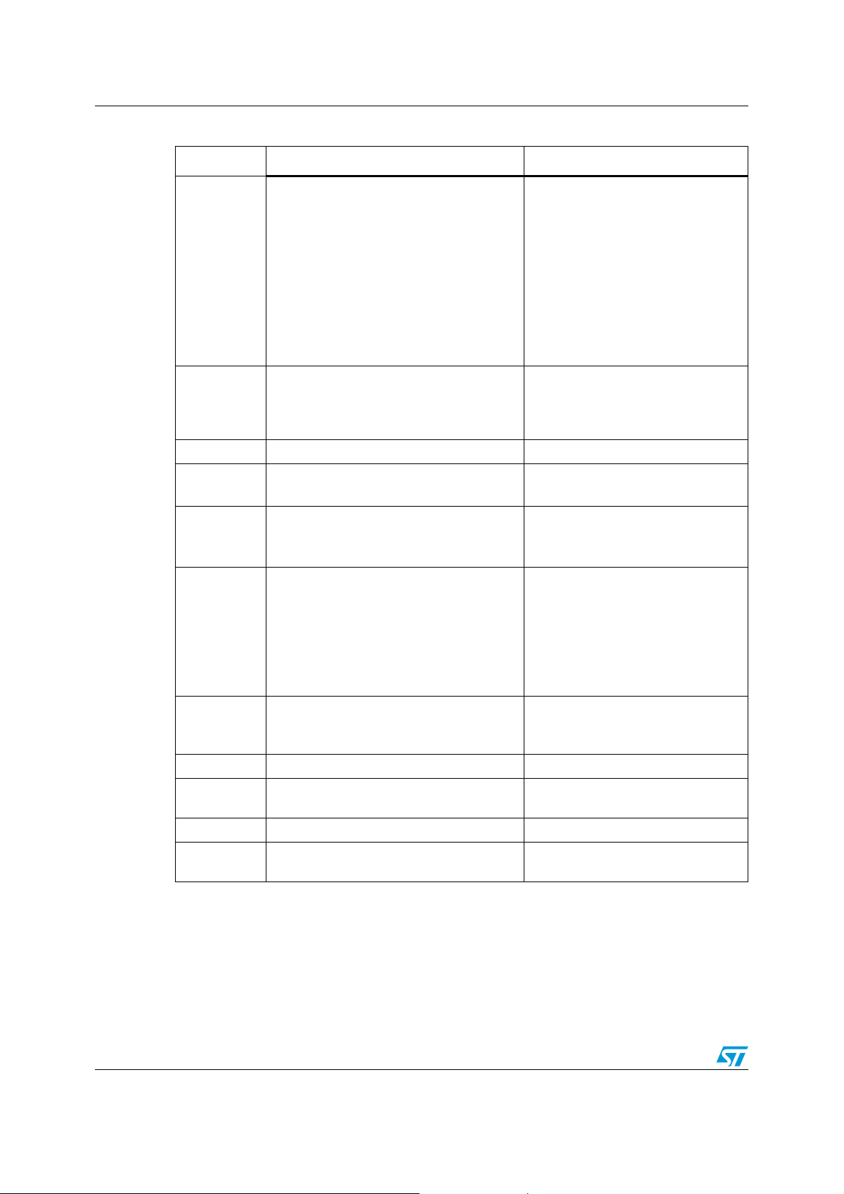
Pin description SPEAr1340
Table 2. Headers/abbreviations (continued)
Header Description Abbreviations
ANA= Analog
OSC= Oscillator
SSTL= SSTL 1V5/1V8
IOTYPE1= 3V3
Pin type Pad type information
IOTYPE2= 3V3/1V8
IOTYPE3= 3V3/2V5
IOTYPE4= 3V3 TTL buffer
REG OUT= Voltage regulator output
ANA REF= Analog reference
DED GND= Dedicated ground
Indicates the presence of an internal pull-up
PU/PD
or pull-down resistor.
Pull-up and pull-down can be enabled or
disabled via software.
Drive Drive current capability –
Slew Signal transition
Direction Indicates the direction of the pad.
Out value Indicates the electrical value on the ball.
The voltage supply that powers the pad.
Supply name
See Table 4: Power supply signals
description.
Reset state Indicates the state during reset –
Reset rel.
state
Indicates the state after reset –
PU= Pull-up
PD= Pull-down
Deact= Deactivated
FAST= Fast slew
NOM= Nominal slew
I= Input
O= Output
IO= Input/output
0= The buffer drives V
OL
1= The buffer drives VOH
H= High-impedance with an active
pull-up resistor
L= High-impedance with an active
pull-down resistor
Z= High-impedance
–
Reset mode IO voltage setting during reset –
Reset rel.
mode
IO voltage setting after reset –
40/194 Doc ID 023063 Rev 2
Page 41

SPEAr1340 Pin description
1234567891011121314
A RTC_XO AIN 4 AIN3 AIN0
ADC_
VREFP
gnd MCLK _XI MCLK_XO
FSMC_IO7/
XGP I O 23 8
FSMC_RSTP
WDWN1/
KBD_COL4/
GPIO_A2
FSMC_IO13/K
BD_ROW 5/X
GPIO5
FSMC_IO8/
KBD_ROW0/X
GPIO0
USB_UOC_D
RVVBUS
MCI F_
DATA2_SD/
XGPIO229
B RTC_XI AIN5 AIN6 AIN1
ADC_
VREFN
gnd
MCLK _
AVDD1V2
MCLK_
AVDD3V3
FSMC_IO6/
XGP I O 23 9
FSMC_IO2/
XGPIO233
FSMC_IO14/K
BD_COL0/ XG
PIO6
FSMC_IO9/
KBD_ROW1/X
GPIO1
USB_UHC0_
DRVVBUS
MCI F_
DATA3_SD/
XGPIO230
C
RTC_
VDD1V5
AIN7 AIN 2
ADC_
AVDD2V5
ADC_AGN D
FSMC_CE0n/
XGPIO249
FSMC_RWPR
T0n/
XGP I O2 46
FSMC_ALE_A
D17/
XGPIO243
FSMC_IO5/
XGP I O 24 0
FSMC_IO1/
XGPIO234
FSMC_IO15/K
BD_COL1/ XG
PIO7
FSMC_IO10/K
BD_ROW2/X
GPIO2
USB_UHC1_
DRVVBUS
MCI F_
DATA4/
XGPIO231
D
USB_UHC1_DPUSB_UH C1_DMUSB_UHC1_
VDD3V3
PLL2_
VDD1V2
gnd
PLL1_
VDD1V2
FSMC_RB0/X
GPIO247
FSMC_REn/X
GPIO244
FSMC_IO4/
XGP I O 24 1
FSMC_IO0/
XGPIO235
FSMC_CE1n/
KBD_COL2/G
PIO_A0
FSMC_IO11/K
BD_ROW3/X
GPIO3
USB_UHC0_
OVERCU R
MCI F_
DATA5/
XGPIO232
E
USB_
ANALOG_
TEST
USB_UH C1_
VDD1V2
USB_UHC1_
VDD2V5
PLL2_
AVDD2V5
gnd
PLL1_
AVDD2V5
FSMC_C LE_A
D16/
XGP I O2 48
FSMC_WEn/
XGPIO245
FSMC_IO3/
XGP I O 24 2
FSMC_RST
PWDWN0/
XGPIO236
FSMC_
RWPRT1n/
KBD_CO L3/
GPIO_A1
FSMC_IO12/K
BD_ROW 4/
XGP I O 4
USB_UHC1_
OVERCU R
MCI F_
DATA0/
XGPIO237
F
USB_UOC_DPUSB_UOC_DMUSB_UOC_V
BUS
USB_UOC_
ID
gnd
VREG2_
2V5_OUT
gnd
IO_
VDD1V8_
3V3
IO_
VDD1V8
_3V3
gnd
IO_
VDD1V8
_3V3_1
IO_
VDD1V8
_3V3_1
gnd
IO_
VDD3V3
G
USB_
TXRTUNE
USB_UOC _V
DD3V3
USB_UOC_V
DD2V5
gnd gnd gnd
H
USB_UHC0_DPUSB_UH C0_DMUSB_
VSSAC
USB_UOC_
VDD1V2
gnd
VREG2
_3V3_IN
J
MIPH Y 0_
VSSR
MIPH Y 0_
VSSR
USB_UHC0_
VDD3V3
USB_UHC0_
VDD2V5
gnd gnd
K
MIPH Y 0_
RXn
MIPH Y 0_
RXp
MIPH Y 0_
VSSR
USB_UHC0_
VDD1V2
gnd
VREG1_
3V3_IN
gnd
IO_COMP_
GND1_
1V8_3V3
IO_COMP_
REXT1_
1V8_3V3
VDD1V2
IO_COMP_
GND2_
1V8_3V3
L
MIPH Y 0_
VSSR
MIPH Y 0_
VSSR
MIPH Y 0_
VDDR1V2
gnd gnd gnd VDD1V2 gnd VDD 1V2 gnd VDD1V2
M
MIPH Y 0_
TXn
MIPH Y 0_
TXp
MIPH Y 0_
VSSR
VDD1V2 gnd
VREG1_
2V5_OUT
gnd V DD1V2 gnd g nd gnd
N
MIPH Y 0_
VDDT1V2
MIPH Y 0_
VDD
PLL1V2
MIPH Y 0_
VSST
gnd
PLL3_
AVDD2V5
gnd VDD1V2 gnd VDD1V2 gnd gnd
P
MIPH Y 0_
XTAL 2
MIPH Y 0_
XTAL 1
MIPH Y 0_
VDD2
PLL2V5
MIPH Y 0_
VSSPLL
gnd
PLL3_
VDD1V2
gnd V DD1V2 gnd g nd gnd
3.1 Pin map
The following figures show the pin map of the device in four quadrants (A, B, C and D).
Figure 2. SPEAr1340 pin map (quadrant A)
Doc ID 023063 Rev 2 41/194
Page 42
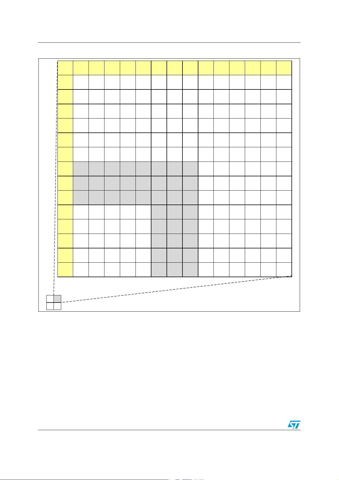
Pin description SPEAr1340
15 16 17 18 19 20 21 2 2 23 24 25 26 27 28
A
MCIF_ADDR1
_CLE_CLK/
XGP I O 22 5
MCIF_LED s/
XGP I O 21 9
MCIF_nC D_
xD/
XGP I O 21 4
FSMC_AD4/M
CIF_nCD_
CF1/
XGP I O 20 9
FSMC_AD9/
MCI F_ nRE S
ET_CF/
XGP I O 20 4
FSMC_AD14/
MCI F_ nDMA C
K_nWP/
XGP I O 19 9
FSMC_AD21/
MCI F_
DATA14/
XGPIO194
LCD_XB5/
ARM_
TRCDATA29/
XGP I O 18 9
LCD_XB0/
ARM_
TRCDATA24/
XGPIO184
LCD_XG3/
ARM_
TRCDATA19/
XGPIO179
LCD_XG0/
ARM_
TRCDATA15/
XGPIO175
LCD_R3/
ARM_
TRC DA TA11/
XGPIO171
LCD_R 6/
ARM_
TRCDATA10/
XGPIO170
LCD_R 7/
ARM_
TRC DA TA5/
XGP I O 16 5
B
MCI F_
DATA7/
XGP I O 22 4
MCI F_
DATA1/
XGP I O 22 0
FSMC_AD0/
MCI F_
ADDR2/
XGP I O 21 5
FSMC_AD5/
MCIF_nC D_
CF2/
XGP I O 21 0
FSMC_AD10/
MCIF_nC S0_
nCE/
XGP I O 20 5
FSMC_AD15/
MCI F_
DATA10/
XGP I O 20 0
FSMC_AD22/
MCI F_
DATA13/
XGPIO195
LCD_XB6/
ARM_
TRCDATA30/
XGP I O 19 0
LCD_XB1/
ARM_
TRCDATA25/
XGPIO185
LCD_XG4/
ARM_
TRCDATA20/
XGPIO180
LCD_XG1/
ARM_
TRCDATA16/
XGPIO176
LCD_R0/
ARM_
TRC DA TA12/
XGPIO172
LCD_VSYNC/
ARM_
TRCDATA8/
XGPIO168
LCD_PE/
ARM_
TRC DA TA4/
XGP I O 16 4
C
MCIF_nC D_
SD_ MMC/
XGP I O 22 6
MCIF_DATA2/
XGP I O 22 1
FSMC_AD1/
MCIF_nC E_
CF/
XGP I O 21 6
FSMC_AD6
/MCIF_DATA_
DIR/
XGP I O 21 1
FSMC_AD11/
MCI F_ CF _
INTR/
XGP I O 20 6
FSMC_AD18/
MCI F_ DATA 9/
XGP I O 20 1
FSMC_AD23/
MCI F_
DATA12/
XGPIO196
LCD_XB7/
ARM_
TRCDATA31/
XGP I O 19 1
LCD_XB2/
ARM_
TRCDATA26/
XGPIO186
LCD_XG5/
ARM_
TRCDATA21/
XGPIO181
LCD_XG2/
ARM_
TRCDATA17/
XGPIO177
LCD_HSY NC
/ARM_
TRC DA TA13/
XGPIO173
LCD_R 1/
ARM_
TRCDATA7/
XGPIO167
LCD_D E/
ARM_
TRC DA TA3/
XGP I O 16 3
D
MCI F_D MAR
Q_RnB_WP/
XGP I O 22 7
MCIF_DATA3/
XGP I O 22 2
FSMC_AD2/
MCIF_nC E_
xD/
XGP I O 21 7
FSMC_AD7/
MCI F_
nIORD_nRE/
XGP I O 21 2
FSMC_AD12/
MCI F_ IOR DY
/XGPIO207
FSMC_AD19/
MCI F_ DATA 8/
XGP I O 20 2
FSMC_AD24/
MCI F_
DATA11/
XGPIO197
FSMC_AD25/
XGP I O 19 2
LCD_XB3/
ARM_
TRCDATA27/
XGPIO187
LCD_XG6/
ARM_
TRCDATA22/
XGPIO182
LCD_LED_P
WM/ARM_
TRCDATA18/
XGPIO178
LCD_XR7/
ARM_
TRC DA TA14/
XGPIO174
LCD_R 4/
ARM_
TRCDATA6/
XGPIO166
LCD_R 5/
ARM_
TRC DA TA1/
XGP I O 16 1
E
MCIF_D ATA1
_SD/
XGP I O 22 8
MCIF_DATA6/
XGP I O 22 3
MCI F_ SD_
CMD/
XGP I O 21 8
MCI F_
ADDR0_ALE/
XGP I O 21 3
FSMC_AD3/
MCI F_ nCE _
SD_MMC/
XGP I O 20 8
FSMC_AD8/
MCIF_nIO
WR_nW E/
XGP I O 20 3
FSMC_AD13/
MCI F_nC S1/
XGPIO198
FSMC_AD20/
MCI F_
DATA15/
XGP I O 19 3
LCD_XB4/
ARM_
TRCDATA28/
XGPIO188
LCD_XG7/
ARM_
TRCDATA23/
XGPIO183
LCD_G0/
ARM_
TRCDATA0/
XGPIO160
LCD_XR0/
ARM_
TRCCTL/
XGPIO159
LCD_XR3/
ARM_TRCCL
K/XGPIO158
LCD_G1/
XGP I O 15 7
F IO_VDD3V3 gnd IO_V DD3V3 IO_VDD 3V3 gnd I O_VDD3V3 IO_VD D3V3 gnd IO_VDD3V3
LCD_R2/
ARM_
TRCDATA2/
XGPIO162
LCD_G4/
XGPIO156
LCD_G6/
XGPIO155
LCD_XR1/
XGPIO154
LCD_XR4/
XGP I O 15 3
G IO_VDD3V3
LCD_G2/
XGPIO152
LCD_G5/
XGPIO151
LCD_G7/
XGPIO150
LCD_XR2/
XGPIO149
LCD_XR5/
XGP I O 14 8
H gnd
LCD_G3/
XGPIO147
LCD_B1/
XGPIO146
LCD_B0/
XGPIO145
LCD_B7/
XGPIO144
LCD_XR6/
XGP I O 14 3
J IO_VDD3V3
LCD_B6/
XGPIO138
LCD_B2/
XGPIO142
LCD_B3/
XGPIO141
LCD_B4/
XGPIO140
LCD_B5/
XGP I O 13 9
K
IO_COMP_
REXT2_1V8_3V3gnd VDD1V2 gnd
IO_COMP_
REXT2_3V3
gnd
CEC1/
XGPIO136
CEC0/
XGPIO135
SPDIF_OUT/X
GPIO137
I2C0_SDA/
XGPIO133
LCD_PC LK/
ARM_
TRC DA TA9/
XGP I O 16 9
L gnd VDD1V2 gnd VDD1V2
IO_COMP_
GND2_3V3
IO_VDD 2V5_
3V3
MAC_TXEN /X
GPIO129
MAC _TXER/ X
GPIO130
MAC_CRS/XG
PIO131
SSP_SS3n/
XGPIO132
I2C0_SCL/
XGP I O 13 4
M gnd gnd VDD1V2 gnd VDD 1V2 gnd
MAC_RXD6/X
GPIO124
MAC_RXD7/X
GPIO125
MAC_COL/
XGPIO126
MAC_RXDV/X
GPIO127
MAC _RXER /X
GPIO128
N gnd gnd gnd VDD1V2 gnd
IO_VDD 2V5_
3V3
MAC_RXD3/X
GPIO119
MAC_RXD4/X
GPIO120
MAC_RXD5/X
GPIO121
MAC _MDC /X
GPIO122
MAC _MDI O/ X
GPIO123
P gnd gnd VDD1V2 gnd
IO_COMP_
REXT_2V5_
3V3
gnd
IO_VDD 2V5_
3V3
MAC_RXD2/X
GPIO118
MAC _TXD6/ X
GPIO115
MAC_TXD7/X
GPIO116
MAC_
RXCLK/
XGP I O 11 7
Figure 3. SPEAr1340 pin map (quadrant B)
42/194 Doc ID 023063 Rev 2
Page 43

SPEAr1340 Pin description
1234567891011121314
R MIPHY0_REF gnd
MIPH Y 0_
VSSR
gnd
MIP HY _
VREG_
3V3_IN
gnd VDD1V2 gnd VDD 1V2 gnd gnd
T DDR_ADDR8
DDR_
RESETn
DDR_CKE gnd gnd
DDRIO_
VDD1V8_1V5
gnd VD D1V2 gnd gnd gnd
U DDR_CS1n DDR_ODT1 DDR_ADDR0 DDR_ADDR9
DDRIO_
VDD1V8_1 V5
gnd
DDRPHY_
VDD1V2
gnd
DDRPHY_
VDD1V2
gnd gnd
V DDR_ADDR7 DDR_ADDR2 DDR_ADDR3
DDR_
ADDR11
gnd
DDRIO_
VDD1V8_1V5
gnd
DDRPHY_
VDD1V2
gnd
DDRPHY_
VDD1V2
gnd
W DDR_ADDR5 DDR_ADDR1 DDR_BA1
DDR_
ADDR14
DDRIO_
VDD1V8_1 V5
gnd
DDRPHY_
VDD1V2
gnd
DDRPHY_
VDD1V2
gnd VD D1V2
Y
DDR_
ADDR13
DDR_ADDR4 DDR_BA0 DDR_ADDR6 gnd
DDRIO_
VDD1V8_1V5
AA DD R_BA2
DDR_
ADDR12
DDR_
ADDR10
DDR_WEn
DDRIO_
VDD1V8_1 V5
gnd
AB DDR_CLKP2 DDR_CLKM2 DDR_CS0n gnd gnd
DDRIO_
VDD1V8_1V5
AC DDR_CLKP1 DDR_CLKM1 DDR_ODT0
DDRIO_VREFDDR_PLL_
AVDD2V5
gnd
DDRIO_
VDD1V8_1V5
gnd
DDRIO_
VDD1V8_1V5
gnd
DDRIO_
VDD1V8_1V5
gnd
DDRIO_
VDD1V8_1V5
gnd
AD DDR_CLKP0 DDR_CLKM0 DDR_RASn DDR_CASn
DDRIO_
COMP_REXT
DDRIO_
VDD1V8_1V5
gnd
DDRIO_
VDD1V8_1V5
gnd
DDRIO_
VDD1V8_1V5
gnd
DDRIO_
VDD1V8_1V5
gnd
DDRIO_
VDD1V8_1 V5
AE DDR_DQ4 DDR_DQ6 DDR_DQS0p DDR_DQ7 DDR_DM0 DDR_DQ5 DDR_DQ20 DDR_DQ16 DDR_DQS2p DDR_DQ17 DDR_DQ19 TEST4 TEST3 TEST2
AF DDR_DQ2 DDR_DQ0 DDR_DQS0n DDR_DQ1 DDR_DQ3 DDR_DQ22 DDR_DQ18 DDR_DQS2n DDR_DQ23 DDR_DM2 DDR_DQ21 TEST1 TEST0 DDR2n_DDR3
AG DDR_DQ11 DDR_DQ13 DDR_DM1 DDR_DQS1n DDR_DQ12 DDR_DQ27 DDR_DQ31 DDR_DM3 D DR_DQS3n DDR_DQ28 DDR_DQ26 Reserved R eserved Reserved
AH DDR_DQ15 DDR_DQ9 DDR_DQ8 DDR_DQS1p DDR_DQ14 DDR_DQ10 DDR_DQ29 DDR_DQ25 DDR_DQ24 DDR_DQS3p DDR_DQ30 Reserved Reserved Reserved
Figure 4. SPEAr1340 pin map (quadrant C)
Doc ID 023063 Rev 2 43/194
Page 44
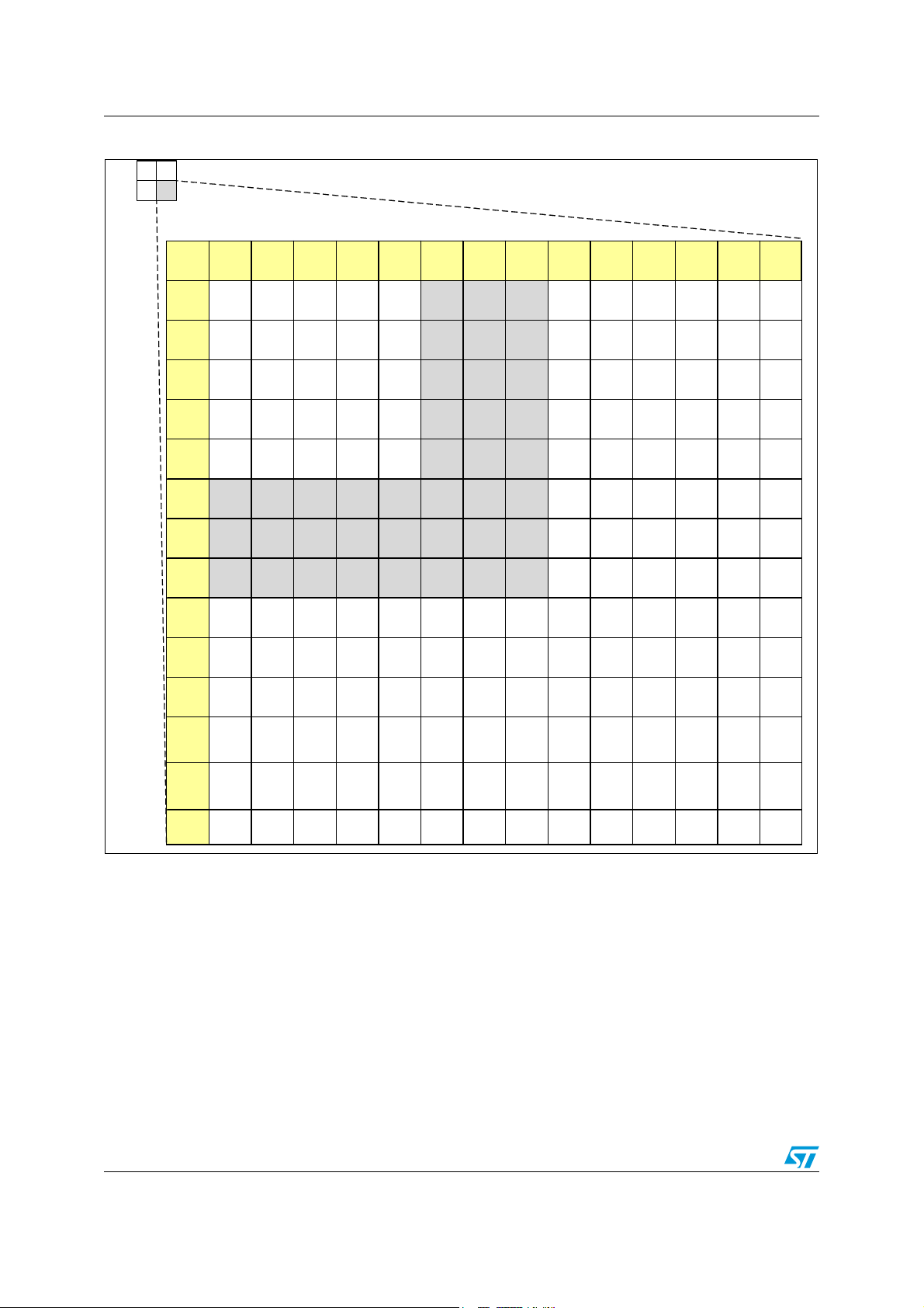
Pin description SPEAr1340
15 16 17 18 1 9 20 21 22 23 24 25 26 27 28
R gnd gnd gnd VD D1V2
IO_COMP_G
ND_2V5_3V3
IO_VDD2V5_
3V3
MAC _
RXD1/
XGP I O 11 4
MAC _
TXD4/
XGPIO110
MAC_
TXD5/
XGP I O 1 1 1
MAC_
RXD0/
XGPIO112
MAC_
GTXCLK/
XGPIO113
T gnd gnd VDD1V2 gnd VDD1V2 gnd
IO_VD D2V5_
3V3
MAC _
TXD3/
XGPIO109
MAC_
TXD1/
XGP I O 1 0 6
MAC_
TXD2/
XGPIO107
MAC_ GTXCL
K125/
XGPIO108
U gnd gnd gnd VD D1V2
OTP_
VDD2V5
IO_VDD3V3
I2S_OUT_WS
/
XGP I O 9 8
I2S_OUT_
DATA3/
XGPIO100
I2S_OUT_
DATA1/
XGP I O 1 0 1
MAC_
TXD0/
XGPIO105
MAC_
TXCLK/
XGPIO104
V VDD1V2 gnd VDD1V2 gnd VDD1V2 gnd
I2S_IN_WS/
XGP I O 9 4
I2S_OUT_
DATA2/
XGPI O 9 5
I2S_OUT_
DATA0/
XGP IO 9 6
I2S_OUT_
REFCLK/
XGPIO102
I2S_OUT_OV
RSAMP_CLK/
XGPIO103
W gnd VDD1V2 gnd VD D1V2 gnd IO_VDD3V 3
I2S_IN_
DATA2/
XGP I O 9 1
I2S_IN_
DATA1/
XGPI O 9 2
I2S_IN_
DATA0/
XGP IO 9 3
I2S_OUT_
BITCLK/
XGP I O 97
I2S_IN_
BITCLK/
XGP I O 99
Y gnd
UART0_
TXD/
XGP I O 8 6
UART0_
RXD/
XGPI O 8 7
UART1_
TXD/
XGP IO 8 8
UART1_
RXD/
XGP I O 89
I2S_IN_
DATA3/
XGP I O 90
AA IO_VDD3V3
SSP_MOSI/
XGP I O 8 1
SSP_MISO/
XGPI O 8 2
SSP_SCK/
XGP IO 8 3
SMI_CS0n/
XGP I O 84
TOUCH_XY_
SEL/
SSP_SS2n/
XGP I O 85
AB gnd
SMI_DATAOU
T/
XGP I O 7 6
SMI_DATA
IN/
XGPI O 7 7
SMI_CS1n/
XGP IO 7 9
SSP_SS0n/
XGP I O 80
SMI_CLK/
XGP I O 78
AC IO_VDD3V3 gnd IO_VD D3V3 gnd IO_VDD3V3 gnd
IO_COMP_
REXT1_3V3
IO_COMP_
GND1_3V3
IO_VDD3V3
VIP_R 11/
CAM1_DATA3
/XGPIO71
VIP_G4/
CAM1_DATA1
/XGPIO72
VIP_G3/
CAM1_
VSYNC/
XGP IO 7 3
VIP_HSYNC/
CAM1_
HSYNC/
XGP I O 74
VIP_R12/
CAM1_
DATA5/
XGP I O 75
AD ARM_TDI ARM_TCK
SPDIF_I N/
GPIO_B3
VIP_B15/
CAM4_
VSYNC/
GPIO_B4
VIP_B11/
CAM4_
HSYNC/
XGP I O 2 6
VIP_B12/
CAM4_DATA0
/XGPIO27
VIP_B8/
CAM4_DATA7
/XGPIO31
VIP_B4/
XGP I O 36
VIP_B5/
XGP I O 41
VIP_R 10/
CAM1_DATA4
/XGPIO66
VIP_G5/
CAM1_DATA2
/XGPIO67
VIP_G2/
CAM1_DATA0
/XGPIO68
VIP_R13/
CAM1_DATA6
/
XGP I O 70
VIP_PIXCLK/
CAM1_
PIXCLK/
XGP I O 69
AE ARM_TRSTn ARM_TMS
UART0_DTRn
/GPT1_
TMR_CPT1/
GPIO_A6
PWM2/
KBD_COL5/
GPIO_B1/
GPIO_WKUP_TR
IG
PWM1/
SSP_SS1n/
XGP I O 2 4
VIP_B13/
CAM4_DATA1
/XGPIO28
VIP_G15/
CAM4_DATA6
/XGPIO32
VIP_B3/
XGP I O 37
VIP_B2/
XGP I O 42
VIP_R 1/
CAM3_
VSYN C/
XGP I O 4 9
VIP_R7/
CAM3_DATA1
/XGPIO53
VIP_G1/
CAM2_DATA1
/XGPIO63
VIP_VSYN C/
CAM2_
VSYNC/
XGP I O 64
VIP_R14/
CAM1_DATA7
/XGPIO65
AF MRESETn AR M_TDO
UART0_RTSn
/GPT1_TMR_
CPT2/
GPIO_A3
UART0_CTSn
/GPT0_
TMR_CLK1/
GPIO_B0
PWM3/
GPT0_TMR _
CPT1/
GPIO_B5/
DDRPHY_VDD1
V2_OFF
VIP_B14/
CAM4_DATA2
/XGPIO29
VIP_G14/
CAM4_DATA5
/XGPIO33
VIP_R4/
XGP I O 38
VIP_R5/
XGP I O 43
VIP_R 6/
CAM3_DATA0
/XGPIO48
VIP_B0/
CAM3_DATA2
/XGPIO52
VIP_R8/
CAM2_DATA5
/XGPIO56
VIP_R9/
CAM2_DATA4
/XGPIO61
VIP_G6/
CAM2_DATA2
/XGPIO62
AG Reserved Reserved
UART0_RIn/
GPT0_TMR_
CPT2/
GPIO_A4
UART0_DCD
n/GPT1_
TMR_CLK2/
GPIO_A7
PWM4/
GPT0_TMR _
CLK2/ GPIO _B6/
DDRIO_VDD1V8
_1V5_OFF
VIP_B9/
CAM4_DATA3
/XGPIO30
VIP_G13/
CAM4_DATA4
/XGPIO34
VIP_G11/
XGP I O 40
VIP_R2/
CAM3_
HSYNC/
XGP I O 44
VIP_B1/
CAM3_DATA3
/XGPIO47
VIP_B7/
CAM3_DATA4
/XGPIO51
VIP_G8/
CAM2_DATA7
/XGPIO55
VIP_DE/
CAM2_
HSYNC/
XGP I O 59
VIP_R15/
CAM2_DATA6
/XGPIO60
AH Reserved Reserved
UART0_DSRn
/GPT1_
TMR_CLK1/
GPIO_A5
I2C1_SDA/
GPIO_B2
I2C1_SCL/
GPIO_B7
VIP_B10/
CAM4_PIXCL
K/XGPIO25
VIP_G12/
XGP IO 3 5
VIP_R3/
CAM3_
PIXCLK/
XGP I O 39
VIP_G10/
CAM3_DATA7
/XGPIO45
VIP_B6/
CAM3_DATA5
/XGPIO46
VIP_G9/
CAM3_DATA6
/XGPIO50
VIP_R0/
CAM2_PIXCL
K/XGPIO54
VIP_G7/
CAM2_DATA3
/XGPIO57
VIP_G0/
CAM2_DATA0
/XGPIO58
Figure 5. SPEAr1340 pin map (quadrant D)
44/194 Doc ID 023063 Rev 2
Page 45
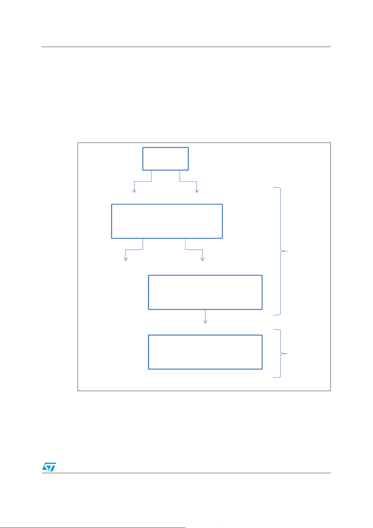
SPEAr1340 Pin description
Pad
Configure the PAD_FUNCTION_EN_x
miscellaneous registers to select between
GPIO/XGPIO or shared IPs.
GPIO/XGPIO Shared IPs
GPIO/XGPIO selected Shared IPsselected
Configure the PAD_SHARED_IP_1
miscellaneous register to select between
IP pin 1 or IP pin 2.
IP pin selected
In case of multiplexed IPs
(1)
, configure the
IP-specific miscellaneous registers to
select which of the available modes to use.
Pad-level
multiplexing
IP-level
multiplexing
3.2 Ball characteristics
Ta bl e 3 provides a detailed description of SPEAr1340 pads and their terminal
characteristics.
Two levels of multiplexing are available:
● Pad-level multiplexing
● IP-level multiplexing
Figure 6 shows an overview of SPEAr1340 multiplexing scheme.
Figure 6. SPEAr1340 multiplexing scheme
1. The multiplexed IPs are: GMAC, Keyboard, MCIF and FSMC. See Section 3.4: Multiplexed signals
description for more details.
Doc ID 023063 Rev 2 45/194
Page 46

46/194 Doc ID 023063 Rev 2
Table 3. Ball characteristics
Ball Pin name
Pin description SPEAr1340
Pad type and pad options Reset/Reset rel. state
Signal type
Pin type
PU/ PD
Drive
Supply name
Direction
Out value
PU/ PD
Drive
Slew
U3 DDR_ADDR0 O SSTL na na na DDRIO_VDD1V8_1V5 O 0 na na na
W2 DDR_ADDR1 O SSTL na na na DDRIO_VDD1V8_1V5 O 0 na na na
V2 DDR_ADDR2 O SSTL na na na DDRIO_VDD1V8_1V5 O 0 na na na
V3 DDR_ADDR3 O SSTL na na na DDRIO_VDD1V8_1V5 O 0 na na na
Y2 DDR_ADDR4 O SSTL na na na DDRIO_VDD1V8_1V5 O 0 na na na
W1 DDR_ADDR5 O SSTL na na na DDRIO_VDD1V8_1V5 O 0 na na na
Y4 DDR_ADDR6 O SSTL na na na DDRIO_VDD1V8_1V5 O 0 na na na
V1 DDR_ADDR7 O SSTL na na na DDRIO_VDD1V8_1V5 O 0 na na na
T1 DDR_ADDR8 O SSTL na na na DDRIO_VDD1V8_1V5 O 0 na na na
U4 DDR_ADDR9 O SSTL na na na DDRIO_VDD1V8_1V5 O 0 na na na
AA3 DDR_ADDR10 O SSTL na na na DDRIO_VDD1V8_1V5 O 0 na na na
V4 DDR_ADDR11 O SSTL na na na DDRIO_VDD1V8_1V5 O 0 na na na
AA2 DDR_ADDR12 O SSTL na na na DDRIO_VDD1V8_1V5 O 0 na na na
Y1 DDR_ADDR13 O SSTL na na na DDRIO_VDD1V8_1V5 O 0 na na na
W4 DDR_ADDR14 O SSTL na na na DDRIO_VDD1V8_1V5 O 0 na na na
AD3 DDR_RASn O SSTL na na na DDRIO_VDD1V8_1V5 O 1 na na na
AD4 DDR_CASn O SSTL na na na DDRIO_VDD1V8_1V5 O 1 na na na
AA4 DDR_WEn O SSTL na na na DDRIO_VDD1V8_1V5 O 1 na na na
AB3 DDR_CS0n O SSTL na na na DDRIO_VDD1V8_1V5 O 1 na na na
U1 DDR_CS1n O SSTL na na na DDRIO_VDD1V8_1V5 O 1 na na na
Y3 DDR_BA0 O SSTL na na na DDRIO_VDD1V8_1V5 O 0 na na na
Slew
Reset mode
DDR2n_DDR3 DDR2n_DDR3
DDR2n_DDR3 DDR2n_DDR3
DDR2n_DDR3 DDR2n_DDR3
DDR2n_DDR3 DDR2n_DDR3
DDR2n_DDR3 DDR2n_DDR3
DDR2n_DDR3 DDR2n_DDR3
DDR2n_DDR3 DDR2n_DDR3
DDR2n_DDR3 DDR2n_DDR3
DDR2n_DDR3 DDR2n_DDR3
DDR2n_DDR3 DDR2n_DDR3
DDR2n_DDR3 DDR2n_DDR3
DDR2n_DDR3 DDR2n_DDR3
DDR2n_DDR3 DDR2n_DDR3
DDR2n_DDR3 DDR2n_DDR3
DDR2n_DDR3 DDR2n_DDR3
DDR2n_DDR3 DDR2n_DDR3
DDR2n_DDR3 DDR2n_DDR3
DDR2n_DDR3 DDR2n_DDR3
DDR2n_DDR3 DDR2n_DDR3
DDR2n_DDR3 DDR2n_DDR3
DDR2n_DDR3 DDR2n_DDR3
Reset rel. mode
Page 47
Table 3. Ball characteristics (continued)
Ball Pin name
SPEAr1340 Pin description
Pad type and pad options Reset/Reset rel. state
Doc ID 023063 Rev 2 47/194
Signal type
W3 DDR_BA1 O SSTL na na na DDRIO_VDD1V8_1V5 O 0 na na na
AA1 DDR_BA2 O SSTL na na na DDRIO_VDD1V8_1V5 O 0 na na na
T3 DDR_CKE O SSTL na na na DDRIO_VDD1V8_1V5 O 0 na na na
AC3 DDR_ODT0 O SSTL na na na DDRIO_VDD1V8_1V5 O 0 na na na
U2 DDR_ODT1 O SSTL na na na DDRIO_VDD1V8_1V5 O 0 na na na
AE5 DDR_DM0 IO SSTL na na na DDRIO_VDD1V8_1V5 I na na na na
AG3 DDR_DM1 IO SSTL na na na DDRIO_VDD1V8_1V5 I na na na na
AF10 DDR_DM2 IO SSTL na na na DDRIO_VDD1V8_1V5 I na na na na
AG8 DDR_DM3 IO SSTL na na na DDRIO_VDD1V8_1V5 I na na na na
AH16 RESERVED IO SSTL na na na DDRIO_VDD1V8_1V5 na na na na na
AE3 DDR_DQS0p IO SSTL na na na DDRIO_VDD1V8_1V5 I na na na na
AF3 DDR_DQS0n IO SSTL na na na DDRIO_VDD1V8_1V5 I na na na na
AH4 DDR_DQS1p IO SSTL na na na DDRIO_VDD1V8_1V5 I na na na na
AG4 DDR_DQS1n IO SSTL na na na DDRIO_VDD1V8_1V5 I na na na na
AE9 DDR_DQS2p IO SSTL na na na DDRIO_VDD1V8_1V5 I na na na na
AF8 DDR_DQS2n IO SSTL na na na DDRIO_VDD1V8_1V5 I na na na na
AH10 DDR_DQS3p IO SSTL na na na DDRIO_VDD1V8_1V5 I na na na na
AG9 DDR_DQS3n IO SSTL na na na DDRIO_VDD1V8_1V5 I na na na na
AG14 RESERVED IO SSTL na na na DDRIO_VDD1V8_1V5 na na na na na na na
AH14 RESERVED IO SSTL na na na DDRIO_VDD1V8_1V5 na na na na na na na
AF2 DDR_DQ0 IO SSTL na na na DDRIO_VDD1V8_1V5 I na na na na
Pin type
PU/ PD
Supply name
Direction
Out value
PU/ PD
Slew
Drive
Drive
Slew
Reset mode
DDR2n_DDR3 DDR2n_DDR3
DDR2n_DDR3 DDR2n_DDR3
DDR2n_DDR3 DDR2n_DDR3
DDR2n_DDR3 DDR2n_DDR3
DDR2n_DDR3 DDR2n_DDR3
DDR2n_DDR3 DDR2n_DDR3
DDR2n_DDR3 DDR2n_DDR3
DDR2n_DDR3 DDR2n_DDR3
DDR2n_DDR3 DDR2n_DDR3
na na
DDR2n_DDR3 DDR2n_DDR3
DDR2n_DDR3 DDR2n_DDR3
DDR2n_DDR3 DDR2n_DDR3
DDR2n_DDR3 DDR2n_DDR3
DDR2n_DDR3 DDR2n_DDR3
DDR2n_DDR3 DDR2n_DDR3
DDR2n_DDR3 DDR2n_DDR3
DDR2n_DDR3 DDR2n_DDR3
DDR2n_DDR3 DDR2n_DDR3
Reset rel. mode
Page 48
48/194 Doc ID 023063 Rev 2
Table 3. Ball characteristics (continued)
Ball Pin name
Pin description SPEAr1340
Pad type and pad options Reset/Reset rel. state
Slew
Signal type
Pin type
PU/ PD
Drive
Supply name
Direction
Out value
PU/ PD
Drive
AF4 DDR_DQ1 IO SSTL na na na DDRIO_VDD1V8_1V5 I na na na na
AF1 DDR_DQ2 IO SSTL na na na DDRIO_VDD1V8_1V5 I na na na na
AF5 DDR_DQ3 IO SSTL na na na DDRIO_VDD1V8_1V5 I na na na na
AE1 DDR_DQ4 IO SSTL na na na DDRIO_VDD1V8_1V5 I na na na na
AE6 DDR_DQ5 IO SSTL na na na DDRIO_VDD1V8_1V5 I na na na na
AE2 DDR_DQ6 IO SSTL na na na DDRIO_VDD1V8_1V5 I na na na na
AE4 DDR_DQ7 IO SSTL na na na DDRIO_VDD1V8_1V5 I na na na na
AH3 DDR_DQ8 IO SSTL na na na DDRIO_VDD1V8_1V5 I na na na na
AH2 DDR_DQ9 IO SSTL na na na DDRIO_VDD1V8_1V5 I na na na na
AH6 DDR_DQ10 IO SSTL na na na DDRIO_VDD1V8_1V5 I na na na na
AG1 DDR_DQ11 IO SSTL na na na DDRIO_VDD1V8_1V5 I na na na na
AG5 DDR_DQ12 IO SSTL na na na DDRIO_VDD1V8_1V5 I na na na na
AG2 DDR_DQ13 IO SSTL na na na DDRIO_VDD1V8_1V5 I na na na na
AH5 DDR_DQ14 IO SSTL na na na DDRIO_VDD1V8_1V5 I na na na na
AH1 DDR_DQ15 IO SSTL na na na DDRIO_VDD1V8_1V5 I na na na na
AE8 DDR_DQ16 IO SSTL na na na DDRIO_VDD1V8_1V5 I na na na na
AE10 DDR_DQ17 IO SSTL na na na DDRIO_VDD1V8_1V5 I na na na na
AF7 DDR_DQ18 IO SSTL na na na DDRIO_VDD1V8_1V5 I na na na na
AE11 DDR_DQ19 IO SSTL na na na DDRIO_VDD1V8_1V5 I na na na na
AE7 DDR_DQ20 IO SSTL na na na DDRIO_VDD1V8_1V5 I na na na na
AF11 DDR_DQ21 IO SSTL na na na DDRIO_VDD1V8_1V5 I na na na na
Slew
Reset mode
DDR2n_DDR3 DDR2n_DDR3
DDR2n_DDR3 DDR2n_DDR3
DDR2n_DDR3 DDR2n_DDR3
DDR2n_DDR3 DDR2n_DDR3
DDR2n_DDR3 DDR2n_DDR3
DDR2n_DDR3 DDR2n_DDR3
DDR2n_DDR3 DDR2n_DDR3
DDR2n_DDR3 DDR2n_DDR3
DDR2n_DDR3 DDR2n_DDR3
DDR2n_DDR3 DDR2n_DDR3
DDR2n_DDR3 DDR2n_DDR3
DDR2n_DDR3 DDR2n_DDR3
DDR2n_DDR3 DDR2n_DDR3
DDR2n_DDR3 DDR2n_DDR3
DDR2n_DDR3 DDR2n_DDR3
DDR2n_DDR3 DDR2n_DDR3
DDR2n_DDR3 DDR2n_DDR3
DDR2n_DDR3 DDR2n_DDR3
DDR2n_DDR3 DDR2n_DDR3
DDR2n_DDR3 DDR2n_DDR3
DDR2n_DDR3 DDR2n_DDR3
Reset rel. mode
Page 49
Table 3. Ball characteristics (continued)
Ball Pin name
SPEAr1340 Pin description
Pad type and pad options Reset/Reset rel. state
Doc ID 023063 Rev 2 49/194
Signal type
AF6 DDR_DQ22 IO SSTL na na na DDRIO_VDD1V8_1V5 I na na na na
AF9 DDR_DQ23 IO SSTL na na na DDRIO_VDD1V8_1V5 I na na na na
AH9 DDR_DQ24 IO SSTL na na na DDRIO_VDD1V8_1V5 I na na na na
AH8 DDR_DQ25 IO SSTL na na na DDRIO_VDD1V8_1V5 I na na na na
AG11 DDR_DQ26 IO SSTL na na na DDRIO_VDD1V8_1V5 I na na na na
AG6 DDR_DQ27 IO SSTL na na na DDRIO_VDD1V8_1V5 I na na na na
AG10 DDR_DQ28 IO SSTL na na na DDRIO_VDD1V8_1V5 I na na na na
AH7 DDR_DQ29 IO SSTL na na na DDRIO_VDD1V8_1V5 I na na na na
AH11 DDR_DQ30 IO SSTL na na na DDRIO_VDD1V8_1V5 I na na na na
AG7 DDR_DQ31 IO SSTL na na na DDRIO_VDD1V8_1V5 I na na na na
AG13 RESERVED IO SSTL na na na DDRIO_VDD1V8_1V5 na na na na na na na
AH13 RESERVED IO SSTL na na na DDRIO_VDD1V8_1V5 na na na na na na na
AG16 RESERVED IO SSTL na na na DDRIO_VDD1V8_1V5 na na na na na na na
AH12 RESERVED IO SSTL na na na DDRIO_VDD1V8_1V5 na na na na na na na
AG15 RESERVED IO SSTL na na na DDRIO_VDD1V8_1V5 na na na na na na na
AG12 RESERVED IO SSTL na na na DDRIO_VDD1V8_1V5 na na na na na na na
AH15 RESERVED IO SSTL na na na DDRIO_VDD1V8_1V5 na na na na na na na
T2 DDR_RESETn O SSTL na na na DDRIO_VDD1V8_1V5 O 0 na na na
AD2 DDR_CLKM0 O SSTL na na na DDRIO_VDD1V8_1V5 O 1 na na na
AD1 DDR_CLKP0 O SSTL na na na DDRIO_VDD1V8_1V5 O 0 na na na
AC2 DDR_CLKM1 O SSTL na na na DDRIO_VDD1V8_1V5 O 1 na na na
Pin type
PU/ PD
Supply name
Direction
Out value
PU/ PD
Slew
Drive
Drive
Slew
Reset mode
DDR2n_DDR3 DDR2n_DDR3
DDR2n_DDR3 DDR2n_DDR3
DDR2n_DDR3 DDR2n_DDR3
DDR2n_DDR3 DDR2n_DDR3
DDR2n_DDR3 DDR2n_DDR3
DDR2n_DDR3 DDR2n_DDR3
DDR2n_DDR3 DDR2n_DDR3
DDR2n_DDR3 DDR2n_DDR3
DDR2n_DDR3 DDR2n_DDR3
DDR2n_DDR3 DDR2n_DDR3
DDR2n_DDR3 DDR2n_DDR3
DDR2n_DDR3 DDR2n_DDR3
DDR2n_DDR3 DDR2n_DDR3
DDR2n_DDR3 DDR2n_DDR3
Reset rel. mode
Page 50

50/194 Doc ID 023063 Rev 2
Table 3. Ball characteristics (continued)
Ball Pin name
Pin description SPEAr1340
Pad type and pad options Reset/Reset rel. state
Signal type
AC1 DDR_CLKP1 O SSTL na na na DDRIO_VDD1V8_1V5 O 0 na na na
AB2 DDR_CLKM2 O SSTL na na na DDRIO_VDD1V8_1V5 O 1 na na na
AB1 DDR_CLKP2 O SSTL na na na DDRIO_VDD1V8_1V5 O 0 na na na
A4 AIN0 I ANA na na na ADC_AVDD2V5 I na na na na na na
B4 AIN1 I ANA na na na ADC_AVDD2V5 I na na na na na na
C3 AIN2 I ANA na na na ADC_AVDD2V5 I na na na na na na
A3 AIN3 I ANA na na na ADC_AVDD2V5 I na na na na na na
A2 AIN4 I ANA na na na ADC_AVDD2V5 I na na na na na na
B2 AIN5 I ANA na na na ADC_AVDD2V5 I na na na na na na
B3 AIN6 I ANA na na na ADC_AVDD2V5 I na na na na na na
C2 AIN7 I ANA na na na ADC_AVDD2V5 I na na na na na na
AF15 MRESETn I IOTYPE1 PU 10ma FAST IO_VDD3V3 I na PU 10ma FAST 3V3 3V3
AF14 DDR2n_DDR3 I IOTYPE1 PU 10ma FAST IO_VDD3V3 I na PU 10ma FAST 3V3 3V3
A1 RTC_XO IO OSC na na na RTC_VDD1V5 na na na na na na na
B1 RTC_XI I OSC na na na RTC_VDD1V5 na na na na na na na
D1 USB_UHC1_DP IO ANA na na na USB_UHC1_VDD3V3 na na na na na na na
D2 USB_UHC1_DM IO ANA na na na USB_UHC1_VDD3V3 na na na na na na na
H1 USB_UHC0_DP IO ANA na na na USB_UHC0_VDD3V3 na na na na na na na
H2 USB_UHC0_DM IO ANA na na na USB_UHC0_VDD3V3 na na na na na na na
F1 USB_UOC_DP IO ANA na na na USB_UOC_VDD3V3 na na na na na na na
F2 USB_UOC_DM IO ANA na na na USB_UOC_VDD3V3 na na na na na na na
Pin type
PU/ PD
Supply name
Direction
Out value
PU/ PD
Slew
Drive
Drive
Slew
Reset mode
DDR2n_DDR3 DDR2n_DDR3
DDR2n_DDR3 DDR2n_DDR3
DDR2n_DDR3 DDR2n_DDR3
Reset rel. mode
Page 51

Table 3. Ball characteristics (continued)
Ball Pin name
SPEAr1340 Pin description
Pad type and pad options Reset/Reset rel. state
Doc ID 023063 Rev 2 51/194
Signal type
F4 USB_UOC_ID I ANA na na na USB_VDD2V5 na na na na na na na
F3 USB_UOC_VBUS IO ANA na na na 5V na na na na na na na
E1 USB_ANALOG_TEST IO ANA na na na USB_VDD2V5 na na na na na na na
A8 MCLK_XO IO OSC na na na MCLK_AVDD3V3 na na na na na na na
A7 MCLK_XI I OSC na na na MCLK_AVDD3V3 na na na na na na na
M2 MIPHY0_TXp O ANA na na na MIPHY0_VDDT1V2 na na na na na na na
M1 MIPHY0_TXn O ANA na na na MIPHY0_VDDT1V2 na na na na na na na
K2 MIPHY0_RXp I ANA na na na MIPHY0_VDDR1V2 na na na na na na na
K1 MIPHY0_RXn I ANA na na na MIPHY0_VDDR1V2 na na na na na na na
P2 MIPHY0_XTAL1 I OSC na na na MIPHY0_VDDPLL1V2 na na na na na na na
P1 MIPHY0_XTAL2 IO OSC na na na MIPHY0_VDDPLL1V2 na na na na na na na
AF13 TEST0 I IOTYPE1 PD 10ma FAST IO_VDD3V3 I L PD 10ma FAST 3V3 3V3
AF12 TEST1 I IOTYPE1 PD 10ma FAST IO_VDD3V3 I L PD 10ma FAST 3V3 3V3
AE14 TEST2 I IOTYPE1 PD 10ma FAST IO_VDD3V3 I L PD 10ma FAST 3V3 3V3
AE13 TEST3 I IOTYPE1 PD 10ma FAST IO_VDD3V3 I L PD 10ma FAST 3V3 3V3
AE12 TEST4 I IOTYPE1 PD 10ma FAST IO_VDD3V3 I L PD 10ma FAST 3V3 3V3
AE15
AD16
AE16
BSD_TRSTn
ARM_TRSTn
BSD_TCK
ARM_TCK
BSD_TMS
ARM_TMS
I IOTYPE1 PU 10ma FAST IO_VDD3V3 I na PU 10ma FAST 3V3 3V3
I IOTYPE1 PU 10ma FAST IO_VDD3V3 I na PU 10ma FAST 3V3 3V3
I IOTYPE1 PU 10ma FAST IO_VDD3V3 I na PU 10ma FAST 3V3 3V3
Pin type
PU/ PD
Supply name
Direction
Out value
PU/ PD
Slew
Drive
Drive
Slew
Reset mode
Reset rel. mode
Page 52

52/194 Doc ID 023063 Rev 2
Table 3. Ball characteristics (continued)
Ball Pin name
Pin description SPEAr1340
Pad type and pad options Reset/Reset rel. state
Signal type
AD15
AF16
A13 USB_UOC_DRVVBUS O IOTYPE1
B13 USB_UHC0_DRVVBUS O IOTYPE1
C13 USB_UHC1_DRVVBUS O IOTYPE1
D13 USB_UHC0_OVERCUR I IOTYPE1 PU 10ma FAST IO_VDD3V3 I na PU 10ma FAST 3V3 3V3
E13 USB_UHC1_OVERCUR I IOTYPE1 PU 10ma FAST IO_VDD3V3 I na PU 10ma FAST 3V3 3V3
A12
B12
C12
D12
BSD_TDI
ARM_TDI
BSD_TDO
ARM_TDO
FSMC_IO8
KBD_ROW0
XGPIO0
FSMC_IO9
KBD_ROW1
XGPIO1
FSMC_IO10
KBD_ROW2
XGPIO2
FSMC_IO11
KBD_ROW3
XGPIO3
I IOTYPE1 PU 10ma FAST IO_VDD3V3 I na PU 10ma FAST 3V3 3V3
IO IOTYPE1
IO
IODIOIOTYPE2
IO
IODIOIOTYPE2
IO
IODIOIOTYPE2
IO
IODIOIOTYPE2
Pin type
PU/ PD
Supply name
Dea
10ma FAST IO_VDD3V3 I na
ct
Dea
10ma FAST IO_VDD3V3 I na
ct
Dea
10ma FAST IO_VDD3V3 O 0
ct
Dea
10ma FAST IO_VDD3V3 O 0
ct
PU/PD4/6/8/
PU/PD4/6/8/
PU/PD4/6/8/
PU/PD4/6/8/
10mA
10mA
10mA
10mA
SLOW
IO_VDD1V8_3V3 I na PU 6ma FAST 1V8 STRAP5
/FAST
SLOW
IO_VDD1V8_3V3 I na PU 6ma FAST 1V8 STRAP5
/FAST
SLOW
IO_VDD1V8_3V3 I na PU 6ma FAST 1V8 STRAP5
/FAST
SLOW
IO_VDD1V8_3V3 I na PU 6ma FAST 1V8 STRAP5
/FAST
Direction
Out value
PU/ PD
Dea
10ma FAST 3V3 3V3
ct
Dea
10ma FAST 3V3 3V3
ct
Dea
10ma FAST 3V3 3V3
ct
Dea
10ma FAST 3V3 3V3
ct
Slew
Drive
Drive
Slew
Reset mode
Reset rel. mode
Page 53
Table 3. Ball characteristics (continued)
Ball Pin name
SPEAr1340 Pin description
Pad type and pad options Reset/Reset rel. state
Doc ID 023063 Rev 2 53/194
E12
A11
B11
C11
D11
E11
A10
AF17
AG17
FSMC_IO12
KBD_ROW4
XGPIO4
FSMC_IO13
KBD_ROW5
XGPIO5
FSMC_IO14
KBD_COL0
XGPIO6
FSMC_IO15
KBD_COL1
XGPIO7
FSMC_CE1n
KBD_COL2
GPIO_A0
FSMC_RWPRT1n
KBD_COL3
GPIO_A1
FSMC_RSTPWDWN1
KBD_COL4
GPIO_A2
UART0_RTSn
GPT1_TMR_CPT2
GPIO_A3
UART0_RIn
GPT0_TMR_CPT2
GPIO_A4
Signal type
IO
IODIOIOTYPE2
IO
IODIOIOTYPE2
IO IOTYPE2
IO IOTYPE2
IO IOTYPE2
IO IOTYPE2
IO IOTYPE2
O
I
IO
I
I
IO
Pin type
IOTYPE1
IOTYPE1
PU/ PD
PU/PD4/6/8/
10mA
PU/PD4/6/8/
10mA
PU/PD4/6/8/
10mA
PU/PD4/6/8/
10mA
PU/PD4/6/8/
10mA
PU/PD4/6/8/
10mA
PU/PD4/6/8/
10mA
PU/PD4/6/8/
10mA
PU/PD4/6/8/
10mA
Drive
Slew
Direction
Supply name
SLOW
IO_VDD1V8_3V3 I na PU 6ma FAST 1V8 STRAP5
/FAST
SLOW
IO_VDD1V8_3V3 I na PU 6ma FAST 1V8 STRAP5
/FAST
SLOW
IO_VDD1V8_3V3 I na PU 6ma FAST 1V8 STRAP5
/FAST
SLOW
IO_VDD1V8_3V3 I na PU 6ma FAST 1V8 STRAP5
/FAST
SLOW
IO_VDD1V8_3V3 I na PU 6ma FAST 1V8 STRAP5
/FAST
SLOW
IO_VDD1V8_3V3 I na PU 6ma FAST 1V8 STRAP5
/FAST
SLOW
IO_VDD1V8_3V3 I na PU 6ma FAST 1V8 STRAP5
/FAST
SLOW
IO_VDD3V3 I na PU 6mA FAST 3V3 3V3
/FAST
SLOW
IO_VDD3V3 I na PU 6mA FAST 3V3 3V3
/FAST
Out value
PU/ PD
Drive
Slew
Reset mode
Reset rel. mode
Page 54

54/194 Doc ID 023063 Rev 2
Table 3. Ball characteristics (continued)
Ball Pin name
Pin description SPEAr1340
Pad type and pad options Reset/Reset rel. state
AH17
AE17
AG18
AF18
AE18
AH18
AD17
AD18
AF19
UART0_DSRn
GPT1_TMR_CLK1
GPIO_A5
UART0_DTRn
GPT1_TMR_CPT1
GPIO_A6
UART0_DCDn
GPT1_TMR_CLK2
GPIO_A7
UART0_CTSn
GPT0_TMR_CLK1
GPIO_B0
PWM2
KBD_COL5
GPIO_B1
GPIO_WKUP_TRIG
I2C1_SDA
GPIO_B2
SPDIF_IN
GPIO_B3
VIP_B15
CAM4_VSYNC
GPIO_B4
PWM3
GPT0_TMR_CPT1
GPIO_B5
DDRPHY_VDD1V2_OFF
Signal type
I
OIOIOTYPE1
O
I
IO
I
OIOIOTYPE1
I
OIOIOTYPE1
O
IO
IO
I
IOD
IO
I
IO
I
I
IO
O
I
IO
O
Pin type
IOTYPE1
IOTYPE1
IOTYPE1
IOTYPE1
IOTYPE1
IOTYPE1
PU/ PD
PU/PD4/6/8/
10mA
PU/PD4/6/8/
10mA
PU/PD4/6/8/
10mA
PU/PD4/6/8/
10mA
PU/PD4/6/8/
10mA
PU/PD4/6/8/
10mA
PU/PD4/6/8/
10mA
PU/PD4/6/8/
10mA
PU/PD4/6/8/
10mA
Drive
Slew
Direction
Supply name
SLOW
IO_VDD3V3 I na PU 6mA FAST 3V3 3V3
/FAST
SLOW
IO_VDD3V3 I na PU 6mA FAST 3V3 3V3
/FAST
SLOW
IO_VDD3V3 I na PU 6mA FAST 3V3 3V3
/FAST
SLOW
IO_VDD3V3 I na PU 6mA FAST 3V3 3V3
/FAST
SLOW
IO_VDD3V3 I na PU 6mA FAST 3V3 3V3
/FAST
SLOW
IO_VDD3V3 I na PU 6mA FAST 3V3 3V3
/FAST
SLOW
IO_VDD3V3 I na PU 6mA FAST 3V3 3V3
/FAST
SLOW
IO_VDD3V3 I na PU 6mA FAST 3V3 3V3
/FAST
SLOW
IO_VDD3V3 I na PU 6mA FAST 3V3 3V3
/FAST
Out value
PU/ PD
Drive
Slew
Reset mode
Reset rel. mode
Page 55
Table 3. Ball characteristics (continued)
Ball Pin name
SPEAr1340 Pin description
Pad type and pad options Reset/Reset rel. state
Doc ID 023063 Rev 2 55/194
AG19
AH19
AE19
AH20
AD19
AD20
AE20
PWM4
GPT0_TMR_CLK2
GPIO_B6
DDRIO_VDD1V8_1V5_OFF
I2C1_SCL
GPIO_B7
PWM1
SSP_SS1n
XGPIO24
STRAP0
VIP_B10
CAM4_PIXCLK
XGPIO25
STRAP1
VIP_B11
CAM4_HSYNC
XGPIO26
STRAP2
VIP_B12
CAM4_DATA0
XGPIO27
STRAP3
VIP_B13
CAM4_DATA1
XGPIO28
STRAP4
O
O
IO
O
IOD
IO
O
O
IO
S
I
I
IO
S
I
I
IO
S
I
I
IO
S
I
I
IO
S
Signal type
Pin type
IOTYPE1
IOTYPE1
IOTYPE1
IOTYPE1
IOTYPE1
IOTYPE1
IOTYPE1
PU/ PD
PU/PD4/6/8/
10mA
PU/PD4/6/8/
10mA
PU/PD4/6/8/
10mA
PU/PD4/6/8/
10mA
PU/PD4/6/8/
10mA
PU/PD4/6/8/
10mA
PU/PD4/6/8/
10mA
Drive
Slew
Direction
Supply name
SLOW
IO_VDD3V3 I na PU 6mA FAST 3V3 3V3
/FAST
SLOW
IO_VDD3V3 I na PU 6mA FAST 3V3 3V3
/FAST
SLOW
IO_VDD3V3 I na PU 6mA FAST 3V3 3V3
/FAST
SLOW
IO_VDD3V3 I na PU 6mA FAST 3V3 3V3
/FAST
SLOW
IO_VDD3V3 I na PU 6mA FAST 3V3 3V3
/FAST
SLOW
IO_VDD3V3 I na PU 6mA FAST 3V3 3V3
/FAST
SLOW
IO_VDD3V3 I na PU 6mA FAST 3V3 3V3
/FAST
Out value
PU/ PD
Drive
Slew
Reset mode
Reset rel. mode
Page 56

56/194 Doc ID 023063 Rev 2
Table 3. Ball characteristics (continued)
Ball Pin name
Pin description SPEAr1340
Pad type and pad options Reset/Reset rel. state
AF20
AG20
AD21
AE21
AF21
AG21
AH21
AD22
AE22
VIP_B14
CAM4_DATA2
XGPIO29
STRAP5
VIP_B9
CAM4_DATA3
XGPIO30
STRAP6
VIP_B8
CAM4_DATA7
XGPIO31
VIP_G15
CAM4_DATA6
XGPIO32
VIP_G14
CAM4_DATA5
XGPIO33
VIP_G13
CAM4_DATA4
XGPIO34
VIP_G12
XGPIO35
VIP_B4
XGPIO36
VIP_B3
XGPIO37
I
I
IO
S
I
I
IO
S
I
I
IO
I
I
IO
I
I
IO
I
I
IO
I
IO
I
IO
I
IO
Signal type
Pin type
IOTYPE1
IOTYPE1
IOTYPE1
IOTYPE1
IOTYPE1
IOTYPE1
IOTYPE1
IOTYPE1
IOTYPE1
PU/ PD
PU/PD4/6/8/
10mA
PU/PD4/6/8/
10mA
PU/PD4/6/8/
10mA
PU/PD4/6/8/
10mA
PU/PD4/6/8/
10mA
PU/PD4/6/8/
10mA
PU/PD4/6/8/
10mA
PU/PD4/6/8/
10mA
PU/PD4/6/8/
10mA
Drive
Slew
Direction
Supply name
SLOW
IO_VDD3V3 I na PU 6mA FAST 3V3 3V3
/FAST
SLOW
IO_VDD3V3 I na PU 6mA FAST 3V3 3V3
/FAST
SLOW
IO_VDD3V3 I na PU 6mA FAST 3V3 3V3
/FAST
SLOW
IO_VDD3V3 I na PU 6mA FAST 3V3 3V3
/FAST
SLOW
IO_VDD3V3 I na PU 6mA FAST 3V3 3V3
/FAST
SLOW
IO_VDD3V3 I na PU 6mA FAST 3V3 3V3
/FAST
SLOW
IO_VDD3V3 I na PU 6mA FAST 3V3 3V3
/FAST
SLOW
IO_VDD3V3 I na PU 6mA FAST 3V3 3V3
/FAST
SLOW
IO_VDD3V3 I na PU 6mA FAST 3V3 3V3
/FAST
Out value
PU/ PD
Drive
Slew
Reset mode
Reset rel. mode
Page 57
Table 3. Ball characteristics (continued)
Ball Pin name
SPEAr1340 Pin description
Pad type and pad options Reset/Reset rel. state
Doc ID 023063 Rev 2 57/194
AF22
AH22
AG22
AD23
AE23
AF23
AG23
AH23
AH24
AG24
VIP_R4
XGPIO38
VIP_R3
CAM3_PIXCLK
XGPIO39
VIP_G11
XGPIO40
VIP_B5
XGPIO41
VIP_B2
XGPIO42
VIP_R5
XGPIO43
VIP_R2
CAM3_HSYNC
XGPIO44
VIP_G10
CAM3_DATA7
XGPIO45
VIP_B6
CAM3_DATA5
XGPIO46
VIP_B1
CAM3_DATA3
XGPIO47
I
IO
I
I
IO
I
IO
I
IO
I
IO
I
IO
I
I
IO
I
I
IO
I
I
IO
I
I
IO
Signal type
Pin type
IOTYPE1
IOTYPE1
IOTYPE1
IOTYPE1
IOTYPE1
IOTYPE1
IOTYPE1
IOTYPE1
IOTYPE1
IOTYPE1
PU/ PD
PU/PD4/6/8/
10mA
PU/PD4/6/8/
10mA
PU/PD4/6/8/
10mA
PU/PD4/6/8/
10mA
PU/PD4/6/8/
10mA
PU/PD4/6/8/
10mA
PU/PD4/6/8/
10mA
PU/PD4/6/8/
10mA
PU/PD4/6/8/
10mA
PU/PD4/6/8/
10mA
Drive
Slew
Direction
Supply name
SLOW
IO_VDD3V3 I na PU 6mA FAST 3V3 3V3
/FAST
SLOW
IO_VDD3V3 I na PU 6mA FAST 3V3 3V3
/FAST
SLOW
IO_VDD3V3 I na PU 6mA FAST 3V3 3V3
/FAST
SLOW
IO_VDD3V3 I na PU 6mA FAST 3V3 3V3
/FAST
SLOW
IO_VDD3V3 I na PU 6mA FAST 3V3 3V3
/FAST
SLOW
IO_VDD3V3 I na PU 6mA FAST 3V3 3V3
/FAST
SLOW
IO_VDD3V3 I na PU 6mA FAST 3V3 3V3
/FAST
SLOW
IO_VDD3V3 I na PU 6mA FAST 3V3 3V3
/FAST
SLOW
IO_VDD3V3 I na PU 6mA FAST 3V3 3V3
/FAST
SLOW
IO_VDD3V3 I na PU 6mA FAST 3V3 3V3
/FAST
Out value
PU/ PD
Drive
Slew
Reset mode
Reset rel. mode
Page 58
58/194 Doc ID 023063 Rev 2
Table 3. Ball characteristics (continued)
Ball Pin name
Pin description SPEAr1340
Pad type and pad options Reset/Reset rel. state
AF24
AE24
AH25
AG25
AF25
AE25
AH26
AG26
AF26
VIP_R6
CAM3_DATA0
XGPIO48
VIP_R1
CAM3_VSYNC
XGPIO49
VIP_G9
CAM3_DATA6
XGPIO50
VIP_B7
CAM3_DATA4
XGPIO51
XGPIO52
VIP_B0
CAM3_DATA2
VIP_R7
CAM3_DATA1
XGPIO53
VIP_R0
CAM2_PIXCLK
XGPIO54
VIP_G8
CAM2_DATA7
XGPIO55
VIP_R8
CAM2_DATA5
XGPIO56
I
I
IO
I
I
IO
I
I
IO
I
I
IO
I
I
IO
I
I
IO
I
I
IO
I
I
IO
I
I
IO
Signal type
Pin type
IOTYPE1
IOTYPE1
IOTYPE1
IOTYPE1
IOTYPE1
IOTYPE1
IOTYPE1
IOTYPE1
IOTYPE1
PU/ PD
PU/PD4/6/8/
10mA
PU/PD4/6/8/
10mA
PU/PD4/6/8/
10mA
PU/PD4/6/8/
10mA
PU/PD4/6/8/
10mA
PU/PD4/6/8/
10mA
PU/PD4/6/8/
10mA
PU/PD4/6/8/
10mA
PU/PD4/6/8/
10mA
Drive
Slew
Direction
Supply name
SLOW
IO_VDD3V3 I na PU 6mA FAST 3V3 3V3
/FAST
SLOW
IO_VDD3V3 I na PU 6mA FAST 3V3 3V3
/FAST
SLOW
IO_VDD3V3 I na PU 6mA FAST 3V3 3V3
/FAST
SLOW
IO_VDD3V3 I na PU 6mA FAST 3V3 3V3
/FAST
SLOW
IO_VDD3V3 I na PU 6mA FAST 3V3 3V3
/FAST
SLOW
IO_VDD3V3 I na PU 6mA FAST 3V3 3V3
/FAST
SLOW
IO_VDD3V3 I na PU 6mA FAST 3V3 3V3
/FAST
SLOW
IO_VDD3V3 I na PU 6mA FAST 3V3 3V3
/FAST
SLOW
IO_VDD3V3 I na PU 6mA FAST 3V3 3V3
/FAST
Out value
PU/ PD
Drive
Slew
Reset mode
Reset rel. mode
Page 59
Table 3. Ball characteristics (continued)
Ball Pin name
SPEAr1340 Pin description
Pad type and pad options Reset/Reset rel. state
Doc ID 023063 Rev 2 59/194
AH27
AH28
AG27
AG28
AF27
AF28
AE26
AE27
AE28
XGPIO57
VIP_G7
CAM2_DATA3
VIP_G0
CAM2_DATA0
XGPIO58
VIP_DE
CAM2_HSYNC
XGPIO59
VIP_R15
CAM2_DATA6
XGPIO60
VIP_R9
CAM2_DATA4
XGPIO61
VIP_G6
CAM2_DATA2
XGPIO62
VIP_G1
CAM2_DATA1
XGPIO63
VIP_VSYNC
CAM2_VSYNC
XGPIO64
VIP_R14
CAM1_DATA7
XGPIO65
I
I
IO
I
I
IO
I
I
IO
I
I
IO
I
I
IO
I
I
IO
I
I
IO
I
I
IO
I
I
IO
Signal type
Pin type
IOTYPE1
IOTYPE1
IOTYPE1
IOTYPE1
IOTYPE1
IOTYPE1
IOTYPE1
IOTYPE1
IOTYPE1
PU/ PD
PU/PD4/6/8/
10mA
PU/PD4/6/8/
10mA
PU/PD4/6/8/
10mA
PU/PD4/6/8/
10mA
PU/PD4/6/8/
10mA
PU/PD4/6/8/
10mA
PU/PD4/6/8/
10mA
PU/PD4/6/8/
10mA
PU/PD4/6/8/
10mA
Drive
Slew
Direction
Supply name
SLOW
IO_VDD3V3 I na PU 6mA FAST 3V3 3V3
/FAST
SLOW
IO_VDD3V3 I na PU 6mA FAST 3V3 3V3
/FAST
SLOW
IO_VDD3V3 I na PU 6mA FAST 3V3 3V3
/FAST
SLOW
IO_VDD3V3 I na PU 6mA FAST 3V3 3V3
/FAST
SLOW
IO_VDD3V3 I na PU 6mA FAST 3V3 3V3
/FAST
SLOW
IO_VDD3V3 I na PU 6mA FAST 3V3 3V3
/FAST
SLOW
IO_VDD3V3 I na PU 6mA FAST 3V3 3V3
/FAST
SLOW
IO_VDD3V3 I na PU 6mA FAST 3V3 3V3
/FAST
SLOW
IO_VDD3V3 I na PU 6mA FAST 3V3 3V3
/FAST
Out value
PU/ PD
Drive
Slew
Reset mode
Reset rel. mode
Page 60

60/194 Doc ID 023063 Rev 2
Table 3. Ball characteristics (continued)
Ball Pin name
Pin description SPEAr1340
Pad type and pad options Reset/Reset rel. state
AD24
AD25
AD26
AD28
AD27
AC24
AC25
AC26
AC27
VIP_R10
CAM1_DATA4
XGPIO66
VIP_G5
CAM1_DATA2
XGPIO67
VIP_G2
CAM1_DATA0
XGPIO68
VIP_PIXCLK
CAM1_PIXCLK
XGPIO69
VIP_R13
CAM1_DATA6
XGPIO70
VIP_R11
CAM1_DATA3
XGPIO71
VIP_G4
CAM1_DATA1
XGPIO72
VIP_G3
CAM1_VSYNC
XGPIO73
VIP_HSYNC
CAM1_HSYNC
XGPIO74
I
I
IO
I
I
IO
I
I
IO
I
I
IO
I
I
IO
I
I
IO
I
I
IO
I
I
IO
I
I
IO
Signal type
Pin type
IOTYPE1
IOTYPE1
IOTYPE1
IOTYPE1
IOTYPE1
IOTYPE1
IOTYPE1
IOTYPE1
IOTYPE1
PU/ PD
PU/PD4/6/8/
10mA
PU/PD4/6/8/
10mA
PU/PD4/6/8/
10mA
PU/PD4/6/8/
10mA
PU/PD4/6/8/
10mA
PU/PD4/6/8/
10mA
PU/PD4/6/8/
10mA
PU/PD4/6/8/
10mA
PU/PD4/6/8/
10mA
Drive
Slew
Direction
Supply name
SLOW
IO_VDD3V3 I na PU 6mA FAST 3V3 3V3
/FAST
SLOW
IO_VDD3V3 I na PU 6mA FAST 3V3 3V3
/FAST
SLOW
IO_VDD3V3 I na PU 6mA FAST 3V3 3V3
/FAST
SLOW
IO_VDD3V3 I na PU 6mA FAST 3V3 3V3
/FAST
SLOW
IO_VDD3V3 I na PU 6mA FAST 3V3 3V3
/FAST
SLOW
IO_VDD3V3 I na PU 6mA FAST 3V3 3V3
/FAST
SLOW
IO_VDD3V3 I na PU 6mA FAST 3V3 3V3
/FAST
SLOW
IO_VDD3V3 I na PU 6mA FAST 3V3 3V3
/FAST
SLOW
IO_VDD3V3 I na PU 6mA FAST 3V3 3V3
/FAST
Out value
PU/ PD
Drive
Slew
Reset mode
Reset rel. mode
Page 61

Table 3. Ball characteristics (continued)
Ball Pin name
SPEAr1340 Pin description
Pad type and pad options Reset/Reset rel. state
Doc ID 023063 Rev 2 61/194
AC28
AB24
AB25
AB28
AB26
AB27
AA24
AA25
AA26
AA27
AA28
Y24
VIP_R12
CAM1_DATA5
XGPIO75
SMI_DATAOUT
XGPIO76
SMI_DATAIN
XGPIO77
SMI_CLK
XGPIO78
SMI_CS1n
XGPIO79
SSP_SS0n
XGPIO80
SSP_MOSI
XGPIO81
SSP_MISO
XGPIO82
SSP_SCK
XGPIO83
SMI_CS0n
XGPIO84
TOUCH_XY_SEL
SSP_SS2n
XGPIO85
UART0_TXD
XGPIO86
Signal type
I
I
IO
O
IO
I
IO
O
IO
O
IO
IO IOTYPE1
IO IOTYPE1
IO IOTYPE1
IO IOTYPE1
O
IO
O
OIOIOTYPE1
O
IO
Pin type
IOTYPE1
IOTYPE1
IOTYPE1
IOTYPE1
IOTYPE1
IOTYPE1
IOTYPE1
PU/ PD
PU/PD4/6/8/
10mA
PU/PD4/6/8/
10mA
PU/PD4/6/8/
10mA
PU/PD4/6/8/
10mA
PU/PD4/6/8/
10mA
PU/PD4/6/8/
10mA
PU/PD4/6/8/
10mA
PU/PD4/6/8/
10mA
PU/PD4/6/8/
10mA
PU/PD4/6/8/
10mA
PU/PD4/6/8/
10mA
PU/PD4/6/8/
10mA
Drive
Slew
Direction
Supply name
SLOW
IO_VDD3V3 I na PU 6mA FAST 3V3 3V3
/FAST
SLOW
IO_VDD3V3 I na PU 6mA FAST 3V3 3V3
/FAST
SLOW
IO_VDD3V3 I na PU 6mA FAST 3V3 3V3
/FAST
SLOW
IO_VDD3V3 I na PU 6mA FAST 3V3 3V3
/FAST
SLOW
IO_VDD3V3 I na PU 6mA FAST 3V3 3V3
/FAST
SLOW
IO_VDD3V3 I na PU 6mA FAST 3V3 3V3
/FAST
SLOW
IO_VDD3V3 I na PU 6mA FAST 3V3 3V3
/FAST
SLOW
IO_VDD3V3 I na PU 6mA FAST 3V3 3V3
/FAST
SLOW
IO_VDD3V3 I na PU 6mA FAST 3V3 3V3
/FAST
SLOW
IO_VDD3V3 I na PU 6mA FAST 3V3 3V3
/FAST
SLOW
IO_VDD3V3 I na PU 6mA FAST 3V3 3V3
/FAST
SLOW
IO_VDD3V3 I na PU 6mA FAST 3V3 3V3
/FAST
Out value
PU/ PD
Drive
Slew
Reset mode
Reset rel. mode
Page 62
62/194 Doc ID 023063 Rev 2
Table 3. Ball characteristics (continued)
Ball Pin name
Pin description SPEAr1340
Pad type and pad options Reset/Reset rel. state
Y25
Y26
Y27
Y28
W24
W25
W26
V24
V25
V26
W27
U24
UART0_RXD
XGPIO87
UART1_TXD
XGPIO88
UART1_RXD
XGPIO89
I2S_IN_DATA3
XGPIO90
I2S_IN_DATA2
XGPIO91
I2S_IN_DATA1
XGPIO92
I2S_IN_DATA0
XGPIO93
I2S_IN_WS
XGPIO94
I2S_OUT_DATA2
XGPIO95
I2S_OUT_DATA0
XGPIO96
I2S_OUT_BITCLK
XGPIO97
I2S_OUT_WS
XGPIO98
I
IO
O
IO
I
IO
I
IO
I
IO
I
IO
I
IO
I
IO
O
IO
O
IO
O
IO
O
IO
Signal type
Pin type
IOTYPE1
IOTYPE1
IOTYPE1
IOTYPE1
IOTYPE1
IOTYPE1
IOTYPE1
IOTYPE1
IOTYPE1
IOTYPE1
IOTYPE1
IOTYPE1
PU/ PD
PU/PD4/6/8/
10mA
PU/PD4/6/8/
10mA
PU/PD4/6/8/
10mA
PU/PD4/6/8/
10mA
PU/PD4/6/8/
10mA
PU/PD4/6/8/
10mA
PU/PD4/6/8/
10mA
PU/PD4/6/8/
10mA
PU/PD4/6/8/
10mA
PU/PD4/6/8/
10mA
PU/PD4/6/8/
10mA
PU/PD4/6/8/
10mA
Drive
Slew
Direction
Supply name
SLOW
IO_VDD3V3 I na PU 6mA FAST 3V3 3V3
/FAST
SLOW
IO_VDD3V3 I na PU 6mA FAST 3V3 3V3
/FAST
SLOW
IO_VDD3V3 I na PU 6mA FAST 3V3 3V3
/FAST
SLOW
IO_VDD3V3 I na PU 6mA FAST 3V3 3V3
/FAST
SLOW
IO_VDD3V3 I na PU 6mA FAST 3V3 3V3
/FAST
SLOW
IO_VDD3V3 I na PU 6mA FAST 3V3 3V3
/FAST
SLOW
IO_VDD3V3 I na PU 6mA FAST 3V3 3V3
/FAST
SLOW
IO_VDD3V3 I na PU 6mA FAST 3V3 3V3
/FAST
SLOW
IO_VDD3V3 I na PU 6mA FAST 3V3 3V3
/FAST
SLOW
IO_VDD3V3 I na PU 6mA FAST 3V3 3V3
/FAST
SLOW
IO_VDD3V3 I na PU 6mA FAST 3V3 3V3
/FAST
SLOW
IO_VDD3V3 I na PU 6mA FAST 3V3 3V3
/FAST
Out value
PU/ PD
Drive
Slew
Reset mode
Reset rel. mode
Page 63
Table 3. Ball characteristics (continued)
Ball Pin name
SPEAr1340 Pin description
Pad type and pad options Reset/Reset rel. state
Doc ID 023063 Rev 2 63/194
W28
U25
U26
V27
V28
U28
U27
T26
T27
T28
T25
R25
I2S_IN_BITCLK
XGPIO99
I2S_OUT_DATA3
XGPIO100
I2S_OUT_DATA1
XGPIO101
I2S_OUT_REFCLK
XGPIO102
I2S_OUT_OVRSAMP_CLK
XGPIO103
MAC_TXCLK
XGPIO104
MAC_TXD0
XGPIO105
MAC_TXD1
XGPIO106
MAC_TXD2
XGPIO107
MAC_GTXCLK125
XGPIO108
MAC_TXD3
XGPIO109
MAC_TXD4
XGPIO110
(1)
I
IO
O
IO
O
IO
I
IO
O
IO
I
IO
O
IO
O
IO
O
IO
I
IO
O
IO
O
IO
Signal type
Pin type
IOTYPE1
IOTYPE1
IOTYPE1
IOTYPE1
IOTYPE1
IOTYPE3
IOTYPE3
IOTYPE3
IOTYPE3
IOTYPE3
IOTYPE3
IOTYPE3
PU/ PD
PU/PD4/6/8/
10mA
PU/PD4/6/8/
10mA
PU/PD4/6/8/
10mA
PU/PD4/6/8/
10mA
PU/PD4/6/8/
10mA
PU/PD4/6/8/
10mA
PU/PD4/6/8/
10mA
PU/PD4/6/8/
10mA
PU/PD4/6/8/
10mA
PU/PD4/6/8/
10mA
PU/PD4/6/8/
10mA
PU/PD4/6/8/
10mA
Drive
Slew
Direction
Supply name
SLOW
IO_VDD3V3 I na PU 6mA FAST 3V3 3V3
/FAST
SLOW
IO_VDD3V3 I na PU 6mA FAST 3V3 3V3
/FAST
SLOW
IO_VDD3V3 I na PU 6mA FAST 3V3 3V3
/FAST
SLOW
IO_VDD3V3 I na PU 6mA FAST 3V3 3V3
/FAST
SLOW
IO_VDD3V3 I na PU 6mA FAST 3V3 3V3
/FAST
SLOW
IO_VDD2V5_3V3 I na PU 6ma FAST 2V5 STRAP6
/FAST
SLOW
IO_VDD2V5_3V3 I na PU 6ma FAST 2V5 STRAP6
/FAST
SLOW
IO_VDD2V5_3V3 I na PU 6ma FAST 2V5 STRAP6
/FAST
SLOW
IO_VDD2V5_3V3 I na PU 6ma FAST 2V5 STRAP6
/FAST
SLOW
IO_VDD2V5_3V3 I na PU 6ma FAST 2V5 STRAP6
/FAST
SLOW
IO_VDD2V5_3V3 I na PU 6ma FAST 2V5 STRAP6
/FAST
SLOW
IO_VDD2V5_3V3 I na PU 6ma FAST 2V5 STRAP6
/FAST
Out value
PU/ PD
Drive
Slew
Reset mode
Reset rel. mode
Page 64

64/194 Doc ID 023063 Rev 2
Table 3. Ball characteristics (continued)
Ball Pin name
Pin description SPEAr1340
Pad type and pad options Reset/Reset rel. state
R26
R27
R28
R24
P26
P27
P28
P25
N24
N25
N26
N27
MAC_TXD5
XGPIO111
MAC_RXD0
XGPIO112
MAC_GTXCLK
XGPIO113
MAC_RXD1
XGPIO114
MAC_TXD6
XGPIO115
MAC_TXD7
XGPIO116
MAC_RXCLK
XGPIO117
MAC_RXD2
XGPIO118
MAC_RXD3
XGPIO119
MAC_RXD4
XGPIO120
MAC_RXD5
XGPIO121
MAC_MDC
XGPIO122
O
IO
I
IO
O
IO
I
IO
O
IO
O
IO
I
IO
I
IO
I
IO
I
IO
I
IO
O
IO
Signal type
Pin type
IOTYPE3
IOTYPE3
IOTYPE3
IOTYPE3
IOTYPE3
IOTYPE3
IOTYPE3
IOTYPE3
IOTYPE3
IOTYPE3
IOTYPE3
IOTYPE3
PU/ PD
PU/PD4/6/8/
10mA
PU/PD4/6/8/
10mA
PU/PD4/6/8/
10mA
PU/PD4/6/8/
10mA
PU/PD4/6/8/
10mA
PU/PD4/6/8/
10mA
PU/PD4/6/8/
10mA
PU/PD4/6/8/
10mA
PU/PD4/6/8/
10mA
PU/PD4/6/8/
10mA
PU/PD4/6/8/
10mA
PU/PD4/6/8/
10mA
Drive
Slew
Direction
Supply name
SLOW
IO_VDD2V5_3V3 I na PU 6ma FAST 2V5 STRAP6
/FAST
SLOW
IO_VDD2V5_3V3 I na PU 6ma FAST 2V5 STRAP6
/FAST
SLOW
IO_VDD2V5_3V3 I na PU 6ma FAST 2V5 STRAP6
/FAST
SLOW
IO_VDD2V5_3V3 I na PU 6ma FAST 2V5 STRAP6
/FAST
SLOW
IO_VDD2V5_3V3 I na PU 6ma FAST 2V5 STRAP6
/FAST
SLOW
IO_VDD2V5_3V3 I na PU 6ma FAST 2V5 STRAP6
/FAST
SLOW
IO_VDD2V5_3V3 I na PU 6ma FAST 2V5 STRAP6
/FAST
SLOW
IO_VDD2V5_3V3 I na PU 6ma FAST 2V5 STRAP6
/FAST
SLOW
IO_VDD2V5_3V3 I na PU 6ma FAST 2V5 STRAP6
/FAST
SLOW
IO_VDD2V5_3V3 I na PU 6ma FAST 2V5 STRAP6
/FAST
SLOW
IO_VDD2V5_3V3 I na PU 6ma FAST 2V5 STRAP6
/FAST
SLOW
IO_VDD2V5_3V3 I na PU 6ma FAST 2V5 STRAP6
/FAST
Out value
PU/ PD
Drive
Slew
Reset mode
Reset rel. mode
Page 65

Table 3. Ball characteristics (continued)
Ball Pin name
SPEAr1340 Pin description
Pad type and pad options Reset/Reset rel. state
Doc ID 023063 Rev 2 65/194
N28
M24
M25
M26
M27
M28
L24
L25
L26
L27
K27
L28
MAC_MDIO
XGPIO123
MAC_RXD6
XGPIO124
MAC_RXD7
XGPIO125
MAC_COL
XGPIO126
MAC_RXDV
XGPIO127
MAC_RXER
XGPIO128
MAC_TXEN
XGPIO129
MAC_TXER
XGPIO130
MAC_CRS
XGPIO131
SSP_SS3n
XGPIO132
I2C0_SDA
XGPIO133
I2C0_SCL
XGPIO134
Signal type
IO IOTYPE3
I
IO
I
IO
I
IO
I
IO
I
IO
O
IO
O
IO
I
IO
O
IO
IOD
IO
IOD
IO
Pin type
IOTYPE3
IOTYPE3
IOTYPE3
IOTYPE3
IOTYPE3
IOTYPE3
IOTYPE3
IOTYPE3
IOTYPE1
IOTYPE1
IOTYPE1
PU/ PD
PU/PD4/6/8/
10mA
PU/PD4/6/8/
10mA
PU/PD4/6/8/
10mA
PU/PD4/6/8/
10mA
PU/PD4/6/8/
10mA
PU/PD4/6/8/
10mA
PU/PD4/6/8/
10mA
PU/PD4/6/8/
10mA
PU/PD4/6/8/
10mA
PU/PD4/6/8/
10mA
PU/PD4/6/8/
10mA
PU/PD4/6/8/
10mA
Drive
Slew
Direction
Supply name
SLOW
IO_VDD2V5_3V3 I na PU 6ma FAST 2V5 STRAP6
/FAST
SLOW
IO_VDD2V5_3V3 I na PU 6ma FAST 2V5 STRAP6
/FAST
SLOW
IO_VDD2V5_3V3 I na PU 6ma FAST 2V5 STRAP6
/FAST
SLOW
IO_VDD2V5_3V3 I na PU 6ma FAST 2V5 STRAP6
/FAST
SLOW
IO_VDD2V5_3V3 I na PU 6ma FAST 2V5 STRAP6
/FAST
SLOW
IO_VDD2V5_3V3 I na PU 6ma FAST 2V5 STRAP6
/FAST
SLOW
IO_VDD2V5_3V3 I na PU 6ma FAST 2V5 STRAP6
/FAST
SLOW
IO_VDD2V5_3V3 I na PU 6ma FAST 2V5 STRAP6
/FAST
SLOW
IO_VDD2V5_3V3 I na PU 6ma FAST 2V5 STRAP6
/FAST
SLOW
IO_VDD3V3 I na PU 6mA FAST 3V3 3V3
/FAST
SLOW
IO_VDD3V3 I na PU 6mA FAST 3V3 3V3
/FAST
SLOW
IO_VDD3V3 I na PU 6mA FAST 3V3 3V3
/FAST
Out value
PU/ PD
Drive
Slew
Reset mode
Reset rel. mode
Page 66

66/194 Doc ID 023063 Rev 2
Table 3. Ball characteristics (continued)
Ball Pin name
Pin description SPEAr1340
Pad type and pad options Reset/Reset rel. state
K25
K24
K26
J24
J28
J27
J26
J25
H28
H27
H26
H25
CEC0
XGPIO135
CEC1
XGPIO136
SPDIF_OUT
XGPIO137
LCD_B6
XGPIO138
LCD_B5
XGPIO139
LCD_B4
XGPIO140
LCD_B3
XGPIO141
LCD_B2
XGPIO142
LCD_XR6
XGPIO143
LCD_B7
XGPIO144
LCD_B0
XGPIO145
LCD_B1
XGPIO146
Signal type
IO IOTYPE1
IO IOTYPE1
O
IO
O
IO
O
IO
O
IO
O
IO
O
IO
O
IO
O
IO
O
IO
O
IO
Pin type
IOTYPE1
IOTYPE1
IOTYPE1
IOTYPE1
IOTYPE1
IOTYPE1
IOTYPE1
IOTYPE1
IOTYPE1
IOTYPE1
PU/ PD
PU/PD4/6/8/
10mA
PU/PD4/6/8/
10mA
PU/PD4/6/8/
10mA
PU/PD4/6/8/
10mA
PU/PD4/6/8/
10mA
PU/PD4/6/8/
10mA
PU/PD4/6/8/
10mA
PU/PD4/6/8/
10mA
PU/PD4/6/8/
10mA
PU/PD4/6/8/
10mA
PU/PD4/6/8/
10mA
PU/PD4/6/8/
10mA
Drive
Slew
Direction
Supply name
SLOW
IO_VDD3V3 I na PU 6mA FAST 3V3 3V3
/FAST
SLOW
IO_VDD3V3 I na PU 6mA FAST 3V3 3V3
/FAST
SLOW
IO_VDD3V3 I na PU 6mA FAST 3V3 3V3
/FAST
SLOW
IO_VDD3V3 I na PU 6mA FAST 3V3 3V3
/FAST
SLOW
IO_VDD3V3 I na PU 6mA FAST 3V3 3V3
/FAST
SLOW
IO_VDD3V3 I na PU 6mA FAST 3V3 3V3
/FAST
SLOW
IO_VDD3V3 I na PU 6mA FAST 3V3 3V3
/FAST
SLOW
IO_VDD3V3 I na PU 6mA FAST 3V3 3V3
/FAST
SLOW
IO_VDD3V3 I na PU 6mA FAST 3V3 3V3
/FAST
SLOW
IO_VDD3V3 I na PU 6mA FAST 3V3 3V3
/FAST
SLOW
IO_VDD3V3 I na PU 6mA FAST 3V3 3V3
/FAST
SLOW
IO_VDD3V3 I na PU 6mA FAST 3V3 3V3
/FAST
Out value
PU/ PD
Drive
Slew
Reset mode
Reset rel. mode
Page 67

Table 3. Ball characteristics (continued)
Ball Pin name
SPEAr1340 Pin description
Pad type and pad options Reset/Reset rel. state
Doc ID 023063 Rev 2 67/194
H24
G28
G27
G26
G25
G24
F28
F27
F26
F25
E28
E27
LCD_G3
XGPIO147
LCD_XR5
XGPIO148
LCD_XR2
XGPIO149
LCD_G7
XGPIO150
LCD_G5
XGPIO151
LCD_G2
XGPIO152
LCD_XR4
XGPIO153
LCD_XR1
XGPIO154
LCD_G6
XGPIO155
LCD_G4
XGPIO156
LCD_G1
XGPIO157
LCD_XR3
ARM_TRCCLK
XGPIO158
Signal type
O
IO
O
IO
O
IO
O
IO
O
IO
O
IO
O
IO
O
IO
O
IO
O
IO
O
IO
O
OIOIOTYPE1
Pin type
IOTYPE1
IOTYPE1
IOTYPE1
IOTYPE1
IOTYPE1
IOTYPE1
IOTYPE1
IOTYPE1
IOTYPE1
IOTYPE1
IOTYPE1
PU/ PD
PU/PD4/6/8/
10mA
PU/PD4/6/8/
10mA
PU/PD4/6/8/
10mA
PU/PD4/6/8/
10mA
PU/PD4/6/8/
10mA
PU/PD4/6/8/
10mA
PU/PD4/6/8/
10mA
PU/PD4/6/8/
10mA
PU/PD4/6/8/
10mA
PU/PD4/6/8/
10mA
PU/PD4/6/8/
10mA
PU/PD4/6/8/
10mA
Drive
Slew
Direction
Supply name
SLOW
IO_VDD3V3 I na PU 6mA FAST 3V3 3V3
/FAST
SLOW
IO_VDD3V3 I na PU 6mA FAST 3V3 3V3
/FAST
SLOW
IO_VDD3V3 I na PU 6mA FAST 3V3 3V3
/FAST
SLOW
IO_VDD3V3 I na PU 6mA FAST 3V3 3V3
/FAST
SLOW
IO_VDD3V3 I na PU 6mA FAST 3V3 3V3
/FAST
SLOW
IO_VDD3V3 I na PU 6mA FAST 3V3 3V3
/FAST
SLOW
IO_VDD3V3 I na PU 6mA FAST 3V3 3V3
/FAST
SLOW
IO_VDD3V3 I na PU 6mA FAST 3V3 3V3
/FAST
SLOW
IO_VDD3V3 I na PU 6mA FAST 3V3 3V3
/FAST
SLOW
IO_VDD3V3 I na PU 6mA FAST 3V3 3V3
/FAST
SLOW
IO_VDD3V3 I na PU 6mA FAST 3V3 3V3
/FAST
SLOW
IO_VDD3V3 I na PU 6mA FAST 3V3 3V3
/FAST
Out value
PU/ PD
Drive
Slew
Reset mode
Reset rel. mode
Page 68
68/194 Doc ID 023063 Rev 2
Table 3. Ball characteristics (continued)
Ball Pin name
Pin description SPEAr1340
Pad type and pad options Reset/Reset rel. state
E26
E25
D28
F24
C28
B28
A28
D27
C27
LCD_XR0
ARM_TRCCTL
XGPIO159
LCD_G0
ARM_TRCDATA0
XGPIO160
LCD_R5
ARM_TRCDATA1
XGPIO161
LCD_R2
ARM_TRCDATA2
XGPIO162
LCD_DE
ARM_TRCDATA3
XGPIO163
LCD_PE
ARM_TRCDATA4
XGPIO164
LCD_R7
ARM_TRCDATA5
XGPIO165
LCD_R4
ARM_TRCDATA6
XGPIO166
LCD_R1
ARM_TRCDATA7
XGPIO167
Signal type
O
OIOIOTYPE1
O
OIOIOTYPE1
O
OIOIOTYPE1
O
OIOIOTYPE1
O
OIOIOTYPE1
O
OIOIOTYPE1
O
OIOIOTYPE1
O
OIOIOTYPE1
O
OIOIOTYPE1
Pin type
PU/ PD
PU/PD4/6/8/
10mA
PU/PD4/6/8/
10mA
PU/PD4/6/8/
10mA
PU/PD4/6/8/
10mA
PU/PD4/6/8/
10mA
PU/PD4/6/8/
10mA
PU/PD4/6/8/
10mA
PU/PD4/6/8/
10mA
PU/PD4/6/8/
10mA
Drive
Slew
Direction
Supply name
SLOW
IO_VDD3V3 I na PU 6mA FAST 3V3 3V3
/FAST
SLOW
IO_VDD3V3 I na PU 6mA FAST 3V3 3V3
/FAST
SLOW
IO_VDD3V3 I na PU 6mA FAST 3V3 3V3
/FAST
SLOW
IO_VDD3V3 I na PU 6mA FAST 3V3 3V3
/FAST
SLOW
IO_VDD3V3 I na PU 6mA FAST 3V3 3V3
/FAST
SLOW
IO_VDD3V3 I na PU 6mA FAST 3V3 3V3
/FAST
SLOW
IO_VDD3V3 I na PU 6mA FAST 3V3 3V3
/FAST
SLOW
IO_VDD3V3 I na PU 6mA FAST 3V3 3V3
/FAST
SLOW
IO_VDD3V3 I na PU 6mA FAST 3V3 3V3
/FAST
Out value
PU/ PD
Drive
Slew
Reset mode
Reset rel. mode
Page 69
Table 3. Ball characteristics (continued)
Ball Pin name
SPEAr1340 Pin description
Pad type and pad options Reset/Reset rel. state
Doc ID 023063 Rev 2 69/194
B27
K28
A27
A26
B26
C26
D26
A25
B25
LCD_VSYNC
ARM_TRCDATA8
XGPIO168
LCD_PCLK
ARM_TRCDATA9
XGPIO169
LCD_R6
ARM_TRCDATA10
XGPIO170
LCD_R3
ARM_TRCDATA11
XGPIO171
LCD_R0
ARM_TRCDATA12
XGPIO172
LCD_HSYNC
ARM_TRCDATA13
XGPIO173
LCD_XR7
ARM_TRCDATA14
XGPIO174
LCD_XG0
ARM_TRCDATA15
XGPIO175
LCD_XG1
ARM_TRCDATA16
XGPIO176
(2)
Signal type
O
OIOIOTYPE1
O IOTYPE4
O
OIOIOTYPE1
O
OIOIOTYPE1
O
OIOIOTYPE1
O
OIOIOTYPE1
O
OIOIOTYPE1
O
OIOIOTYPE1
O
OIOIOTYPE1
Pin type
PU/ PD
Direction
Supply name
PU/PD4/6/8/
PU/
PD
PU/PD4/6/8/
PU/PD4/6/8/
PU/PD4/6/8/
PU/PD4/6/8/
PU/PD4/6/8/
PU/PD4/6/8/
PU/PD4/6/8/
SLOW
10mA
8 mA na IO_VDD3V3 I na PU 8mA na 3V3 3V3
10mA
10mA
10mA
10mA
10mA
10mA
10mA
IO_VDD3V3 I na PU 6mA FAST 3V3 3V3
/FAST
SLOW
IO_VDD3V3 I na PU 6mA FAST 3V3 3V3
/FAST
SLOW
IO_VDD3V3 I na PU 6mA FAST 3V3 3V3
/FAST
SLOW
IO_VDD3V3 I na PU 6mA FAST 3V3 3V3
/FAST
SLOW
IO_VDD3V3 I na PU 6mA FAST 3V3 3V3
/FAST
SLOW
IO_VDD3V3 I na PU 6mA FAST 3V3 3V3
/FAST
SLOW
IO_VDD3V3 I na PU 6mA FAST 3V3 3V3
/FAST
SLOW
IO_VDD3V3 I na PU 6mA FAST 3V3 3V3
/FAST
Out value
PU/ PD
Slew
Drive
Drive
Slew
Reset mode
Reset rel. mode
Page 70

70/194 Doc ID 023063 Rev 2
Table 3. Ball characteristics (continued)
Ball Pin name
Pin description SPEAr1340
Pad type and pad options Reset/Reset rel. state
C25
D25
A24
B24
C24
D24
E24
A23
B23
LCD_XG2
ARM_TRCDATA17
XGPIO177
LCD_LED_PWM
ARM_TRCDATA18
XGPIO178
LCD_XG3
ARM_TRCDATA19
XGPIO179
LCD_XG4
ARM_TRCDATA20
XGPIO180
LCD_XG5
ARM_TRCDATA21
XGPIO181
LCD_XG6
ARM_TRCDATA22
XGPIO182
LCD_XG7
ARM_TRCDATA23
XGPIO183
LCD_XB0
ARM_TRCDATA24
XGPIO184
LCD_XB1
ARM_TRCDATA25
XGPIO185
Signal type
O
OIOIOTYPE1
O
OIOIOTYPE1
O
OIOIOTYPE1
O
OIOIOTYPE1
O
OIOIOTYPE1
O
OIOIOTYPE1
O
OIOIOTYPE1
O
OIOIOTYPE1
O
OIOIOTYPE1
Pin type
PU/ PD
PU/PD4/6/8/
10mA
PU/PD4/6/8/
10mA
PU/PD4/6/8/
10mA
PU/PD4/6/8/
10mA
PU/PD4/6/8/
10mA
PU/PD4/6/8/
10mA
PU/PD4/6/8/
10mA
PU/PD4/6/8/
10mA
PU/PD4/6/8/
10mA
Drive
Slew
Direction
Supply name
SLOW
IO_VDD3V3 I na PU 6mA FAST 3V3 3V3
/FAST
SLOW
IO_VDD3V3 I na PU 6mA FAST 3V3 3V3
/FAST
SLOW
IO_VDD3V3 I na PU 6mA FAST 3V3 3V3
/FAST
SLOW
IO_VDD3V3 I na PU 6mA FAST 3V3 3V3
/FAST
SLOW
IO_VDD3V3 I na PU 6mA FAST 3V3 3V3
/FAST
SLOW
IO_VDD3V3 I na PU 6mA FAST 3V3 3V3
/FAST
SLOW
IO_VDD3V3 I na PU 6mA FAST 3V3 3V3
/FAST
SLOW
IO_VDD3V3 I na PU 6mA FAST 3V3 3V3
/FAST
SLOW
IO_VDD3V3 I na PU 6mA FAST 3V3 3V3
/FAST
Out value
PU/ PD
Drive
Slew
Reset mode
Reset rel. mode
Page 71

Table 3. Ball characteristics (continued)
Ball Pin name
SPEAr1340 Pin description
Pad type and pad options Reset/Reset rel. state
Doc ID 023063 Rev 2 71/194
C23
D23
E23
A22
B22
C22
D22
E22
A21
LCD_XB2
ARM_TRCDATA26
XGPIO186
LCD_XB3
ARM_TRCDATA27
XGPIO187
LCD_XB4
ARM_TRCDATA28
XGPIO188
LCD_XB5
ARM_TRCDATA29
XGPIO189
LCD_XB6
ARM_TRCDATA30
XGPIO190
LCD_XB7
ARM_TRCDATA31
XGPIO191
FSMC_AD25
XGPIO192
FSMC_AD20
MCIF_DATA15
XGPIO193
FSMC_AD21
MCIF_DATA14
XGPIO194
Signal type
O
OIOIOTYPE1
O
OIOIOTYPE1
O
OIOIOTYPE1
O
OIOIOTYPE1
O
OIOIOTYPE1
O
OIOIOTYPE1
O
IO
O
IOIOIOTYPE1
O
IOIOIOTYPE1
Pin type
IOTYPE1
PU/ PD
PU/PD4/6/8/
10mA
PU/PD4/6/8/
10mA
PU/PD4/6/8/
10mA
PU/PD4/6/8/
10mA
PU/PD4/6/8/
10mA
PU/PD4/6/8/
10mA
PU/PD4/6/8/
10mA
PU/PD4/6/8/
10mA
PU/PD4/6/8/
10mA
Drive
Slew
Direction
Supply name
SLOW
IO_VDD3V3 I na PU 6mA FAST 3V3 3V3
/FAST
SLOW
IO_VDD3V3 I na PU 6mA FAST 3V3 3V3
/FAST
SLOW
IO_VDD3V3 I na PU 6mA FAST 3V3 3V3
/FAST
SLOW
IO_VDD3V3 I na PU 6mA FAST 3V3 3V3
/FAST
SLOW
IO_VDD3V3 I na PU 6mA FAST 3V3 3V3
/FAST
SLOW
IO_VDD3V3 I na PU 6mA FAST 3V3 3V3
/FAST
SLOW
IO_VDD3V3 I na PU 6mA FAST 3V3 3V3
/FAST
SLOW
IO_VDD3V3 I na PU 6mA FAST 3V3 3V3
/FAST
SLOW
IO_VDD3V3 I na PU 6mA FAST 3V3 3V3
/FAST
Out value
PU/ PD
Drive
Slew
Reset mode
Reset rel. mode
Page 72

72/194 Doc ID 023063 Rev 2
Table 3. Ball characteristics (continued)
Ball Pin name
Pin description SPEAr1340
Pad type and pad options Reset/Reset rel. state
B21
C21
D21
E21
A20
B20
C20
D20
E20
FSMC_AD22
MCIF_DATA13
XGPIO195
FSMC_AD23
MCIF_DATA12
XGPIO196
FSMC_AD24
MCIF_DATA11
XGPIO197
FSMC_AD13
MCIF_nCS1
XGPIO198
FSMC_AD14
MCIF_nDMACK_nWP
XGPIO199
FSMC_AD15
MCIF_DATA10
XGPIO200
FSMC_AD18
MCIF_DATA9
XGPIO201
FSMC_AD19
MCIF_DATA8
XGPIO202
FSMC_AD8
MCIF_nIOWR_nWE
XGPIO203
Signal type
O
IOIOIOTYPE1
O
IOIOIOTYPE1
O
IOIOIOTYPE1
O
OIOIOTYPE1
O
OIOIOTYPE1
O
IOIOIOTYPE1
O
IOIOIOTYPE1
O
IOIOIOTYPE1
O
OIOIOTYPE1
Pin type
PU/ PD
PU/PD4/6/8/
10mA
PU/PD4/6/8/
10mA
PU/PD4/6/8/
10mA
PU/PD4/6/8/
10mA
PU/PD4/6/8/
10mA
PU/PD4/6/8/
10mA
PU/PD4/6/8/
10mA
PU/PD4/6/8/
10mA
PU/PD4/6/8/
10mA
Drive
Slew
Direction
Supply name
SLOW
IO_VDD3V3 I na PU 6mA FAST 3V3 3V3
/FAST
SLOW
IO_VDD3V3 I na PU 6mA FAST 3V3 3V3
/FAST
SLOW
IO_VDD3V3 I na PU 6mA FAST 3V3 3V3
/FAST
SLOW
IO_VDD3V3 I na PU 6mA FAST 3V3 3V3
/FAST
SLOW
IO_VDD3V3 I na PU 6mA FAST 3V3 3V3
/FAST
SLOW
IO_VDD3V3 I na PU 6mA FAST 3V3 3V3
/FAST
SLOW
IO_VDD3V3 I na PU 6mA FAST 3V3 3V3
/FAST
SLOW
IO_VDD3V3 I na PU 6mA FAST 3V3 3V3
/FAST
SLOW
IO_VDD3V3 I na PU 6mA FAST 3V3 3V3
/FAST
Out value
PU/ PD
Drive
Slew
Reset mode
Reset rel. mode
Page 73
Table 3. Ball characteristics (continued)
Ball Pin name
SPEAr1340 Pin description
Pad type and pad options Reset/Reset rel. state
Doc ID 023063 Rev 2 73/194
A19
B19
C19
D19
E19
A18
B18
C18
D18
FSMC_AD9
MCIF_nRESET_CF
XGPIO204
FSMC_AD10
MCIF_nCS0_nCE
XGPIO205
FSMC_AD11
MCIF_CF_INTR
XGPIO206
FSMC_AD12
MCIF_IORDY
XGPIO207
FSMC_AD3
MCIF_nCE_SD_MMC
XGPIO208
FSMC_AD4
MCIF_nCD_CF1
XGPIO209
FSMC_AD5
MCIF_nCD_CF2
XGPIO210
FSMC_AD6
MCIF_DATA_DIR
XGPIO211
FSMC_AD7
MCIF_nIORD_nRE
XGPIO212
Signal type
O
OIOIOTYPE1
O
OIOIOTYPE1
O
I
IO
O
I
IO
O
OIOIOTYPE1
O
I
IO
O
I
IO
O
OIOIOTYPE1
O
OIOIOTYPE1
Pin type
IOTYPE1
IOTYPE1
IOTYPE1
IOTYPE1
PU/ PD
PU/PD4/6/8/
10mA
PU/PD4/6/8/
10mA
PU/PD4/6/8/
10mA
PU/PD4/6/8/
10mA
PU/PD4/6/8/
10mA
PU/PD4/6/8/
10mA
PU/PD4/6/8/
10mA
PU/PD4/6/8/
10mA
PU/PD4/6/8/
10mA
Drive
Slew
Direction
Supply name
SLOW
IO_VDD3V3 I na PU 6mA FAST 3V3 3V3
/FAST
SLOW
IO_VDD3V3 I na PU 6mA FAST 3V3 3V3
/FAST
SLOW
IO_VDD3V3 I na PU 6mA FAST 3V3 3V3
/FAST
SLOW
IO_VDD3V3 I na PU 6mA FAST 3V3 3V3
/FAST
SLOW
IO_VDD3V3 I na PU 6mA FAST 3V3 3V3
/FAST
SLOW
IO_VDD3V3 I na PU 6mA FAST 3V3 3V3
/FAST
SLOW
IO_VDD3V3 I na PU 6mA FAST 3V3 3V3
/FAST
SLOW
IO_VDD3V3 I na PU 6mA FAST 3V3 3V3
/FAST
SLOW
IO_VDD3V3 I na PU 6mA FAST 3V3 3V3
/FAST
Out value
PU/ PD
Drive
Slew
Reset mode
Reset rel. mode
Page 74

74/194 Doc ID 023063 Rev 2
Table 3. Ball characteristics (continued)
Ball Pin name
Pin description SPEAr1340
Pad type and pad options Reset/Reset rel. state
E18
A17
B17
C17
D17
E17
A16
B16
C16
D16
E16
MCIF_ADDR0_ALE
XGPIO213
MCIF_nCD_xD
XGPIO214
FSMC_AD0
MCIF_ADDR2
XGPIO215
FSMC_AD1
MCIF_nCE_CF
XGPIO216
FSMC_AD2
MCIF_nCE_xD
XGPIO217
MCIF_SD_CMD
XGPIO218
MCIF_LEDS
XGPIO219
MCIF_DATA1
XGPIO220
MCIF_DATA2
XGPIO221
MCIF_DATA3
XGPIO222
MCIF_DATA6
XGPIO223
Signal type
O
IO
I
IO
O
OIOIOTYPE1
O
OIOIOTYPE1
O
OIOIOTYPE1
IO IOTYPE1
O
IO
IO IOTYPE1
IO IOTYPE1
IO IOTYPE1
IO IOTYPE1
Pin type
IOTYPE1
IOTYPE1
IOTYPE1
PU/ PD
PU/PD4/6/8/
10mA
PU/PD4/6/8/
10mA
PU/PD4/6/8/
10mA
PU/PD4/6/8/
10mA
PU/PD4/6/8/
10mA
PU/PD4/6/8/
10mA
PU/PD4/6/8/
10mA
PU/PD4/6/8/
10mA
PU/PD4/6/8/
10mA
PU/PD4/6/8/
10mA
PU/PD4/6/8/
10mA
Drive
Slew
Direction
Supply name
SLOW
IO_VDD3V3 I na PU 6mA FAST 3V3 3V3
/FAST
SLOW
IO_VDD3V3 I na PU 6mA FAST 3V3 3V3
/FAST
SLOW
IO_VDD3V3 I na PU 6mA FAST 3V3 3V3
/FAST
SLOW
IO_VDD3V3 I na PU 6mA FAST 3V3 3V3
/FAST
SLOW
IO_VDD3V3 I na PU 6mA FAST 3V3 3V3
/FAST
SLOW
IO_VDD3V3 I na PU 6mA FAST 3V3 3V3
/FAST
SLOW
IO_VDD3V3 I na PU 6mA FAST 3V3 3V3
/FAST
SLOW
IO_VDD3V3 I na PU 6mA FAST 3V3 3V3
/FAST
SLOW
IO_VDD3V3 I na PU 6mA FAST 3V3 3V3
/FAST
SLOW
IO_VDD3V3 I na PU 6mA FAST 3V3 3V3
/FAST
SLOW
IO_VDD3V3 I na PU 6mA FAST 3V3 3V3
/FAST
Out value
PU/ PD
Drive
Slew
Reset mode
Reset rel. mode
Page 75
Table 3. Ball characteristics (continued)
Ball Pin name
SPEAr1340 Pin description
Pad type and pad options Reset/Reset rel. state
Doc ID 023063 Rev 2 75/194
B15
A15
C15
D15
E15
A14
B14
C14
D14
B10
C10
D10
MCIF_DATA7
XGPIO224
MCIF_ADDR1_CLE_CLK
XGPIO225
MCIF_nCD_SD_MMC
XGPIO226
MCIF_DMARQ_RnB_WP
XGPIO227
MCIF_DATA1_SD
XGPIO228
MCIF_DATA2_SD
XGPIO229
MCIF_DATA3_SD
XGPIO230
MCIF_DATA4
XGPIO231
MCIF_DATA5
XGPIO232
FSMC_IO2
XGPIO233
FSMC_IO1
XGPIO234
FSMC_IO0
XGPIO235
Signal type
IO IOTYPE1
O
IO
I
IO
I
IO
IO IOTYPE1
IO IOTYPE1
IO IOTYPE1
IO IOTYPE1
IO IOTYPE1
IO IOTYPE2
IO IOTYPE2
IO IOTYPE2
Pin type
IOTYPE1
IOTYPE1
IOTYPE1
PU/ PD
PU/PD4/6/8/
10mA
PU/PD4/6/8/
10mA
PU/PD4/6/8/
10mA
PU/PD4/6/8/
10mA
PU/PD4/6/8/
10mA
PU/PD4/6/8/
10mA
PU/PD4/6/8/
10mA
PU/PD4/6/8/
10mA
PU/PD4/6/8/
10mA
PU/PD4/6/8/
10mA
PU/PD4/6/8/
10mA
PU/PD4/6/8/
10mA
Drive
Slew
Direction
Supply name
SLOW
IO_VDD3V3 I na PU 6mA FAST 3V3 3V3
/FAST
SLOW
IO_VDD3V3 I na PU 6mA FAST 3V3 3V3
/FAST
SLOW
IO_VDD3V3 I na PU 6mA FAST 3V3 3V3
/FAST
SLOW
IO_VDD3V3 I na PU 6mA FAST 3V3 3V3
/FAST
SLOW
IO_VDD3V3 I na PU 6mA FAST 3V3 3V3
/FAST
SLOW
IO_VDD3V3 I na PU 6mA FAST 3V3 3V3
/FAST
SLOW
IO_VDD3V3 I na PU 6mA FAST 3V3 3V3
/FAST
SLOW
IO_VDD3V3 I na PU 6mA FAST 3V3 3V3
/FAST
SLOW
IO_VDD3V3 I na PU 6mA FAST 3V3 3V3
/FAST
SLOW
IO_VDD1V8_3V3 I na PU 6ma FAST 1V8 STRAP4
/FAST
SLOW
IO_VDD1V8_3V3 I na PU 6ma FAST 1V8 STRAP4
/FAST
SLOW
IO_VDD1V8_3V3 I na PU 6ma FAST 1V8 STRAP4
/FAST
Out value
PU/ PD
Drive
Slew
Reset mode
Reset rel. mode
Page 76

76/194 Doc ID 023063 Rev 2
Table 3. Ball characteristics (continued)
Ball Pin name
Pin description SPEAr1340
Pad type and pad options Reset/Reset rel. state
E10
E14
A9
B9
C9
D9
E9
C8
D8
E8
C7
D7
FSMC_RSTPWDWN0
XGPIO236
MCIF_DATA0
XGPIO237
FSMC_IO7
XGPIO238
FSMC_IO6
XGPIO239
FSMC_IO5
XGPIO240
FSMC_IO4
XGPIO241
FSMC_IO3
XGPIO242
FSMC_ALE_AD17
XGPIO243
FSMC_REn
XGPIO244
FSMC_WEn
XGPIO245
FSMC_RWPRT0n
XGPIO246
FSMC_RB0
XGPIO247
Signal type
O
IO
IO IOTYPE1
IO IOTYPE2
IO IOTYPE2
IO IOTYPE2
IO IOTYPE2
IO IOTYPE2
O
IO
O
IO
O
IO
O
IO
IO IOTYPE2
Pin type
IOTYPE2
IOTYPE2
IOTYPE2
IOTYPE2
IOTYPE2
PU/ PD
PU/PD4/6/8/
10mA
PU/PD4/6/8/
10mA
PU/PD4/6/8/
10mA
PU/PD4/6/8/
10mA
PU/PD4/6/8/
10mA
PU/PD4/6/8/
10mA
PU/PD4/6/8/
10mA
PU/PD4/6/8/
10mA
PU/PD4/6/8/
10mA
PU/PD4/6/8/
10mA
PU/PD4/6/8/
10mA
PU/PD4/6/8/
10mA
Drive
Slew
Direction
Supply name
SLOW
IO_VDD1V8_3V3 I na PU 6ma FAST 1V8 STRAP4
/FAST
SLOW
IO_VDD3V3 I na PU 6mA FAST 3V3 3V3
/FAST
SLOW
IO_VDD1V8_3V3 I na PU 6ma FAST 1V8 STRAP4
/FAST
SLOW
IO_VDD1V8_3V3 I na PU 6ma FAST 1V8 STRAP4
/FAST
SLOW
IO_VDD1V8_3V3 I na PU 6ma FAST 1V8 STRAP4
/FAST
SLOW
IO_VDD1V8_3V3 I na PU 6ma FAST 1V8 STRAP4
/FAST
SLOW
IO_VDD1V8_3V3 I na PU 6ma FAST 1V8 STRAP4
/FAST
SLOW
IO_VDD1V8_3V3 I na PU 6ma FAST 1V8 STRAP4
/FAST
SLOW
IO_VDD1V8_3V3 I na PU 6ma FAST 1V8 STRAP4
/FAST
SLOW
IO_VDD1V8_3V3 I na PU 6ma FAST 1V8 STRAP4
/FAST
SLOW
IO_VDD1V8_3V3 I na PU 6ma FAST 1V8 STRAP4
/FAST
SLOW
IO_VDD1V8_3V3 I na PU 6ma FAST 1V8 STRAP4
/FAST
Out value
PU/ PD
Drive
Slew
Reset mode
Reset rel. mode
Page 77
Table 3. Ball characteristics (continued)
Ball Pin name
SPEAr1340 Pin description
Pad type and pad options Reset/Reset rel. state
Doc ID 023063 Rev 2 77/194
E7
C6
C1 RTC_VDD1V5 PWR
K13
K17
L10
L12
L14
L16
L18
M11
M17
M19
N10
N12
N18
P11
P17
FSMC_CLE_AD16
XGPIO248
FSMC_CE0n
XGPIO249
VDD1V2 PWR
O
IO
O
IO
Signal type
Pin type
IOTYPE2
IOTYPE2
PU/ PD
PU/PD4/6/8/
10mA
PU/PD4/6/8/
10mA
Drive
Slew
Direction
Supply name
SLOW
IO_VDD1V8_3V3 I na PU 6ma FAST 1V8 STRAP4
/FAST
SLOW
IO_VDD1V8_3V3 I na PU 6ma FAST 1V8 STRAP4
/FAST
Out value
PU/ PD
Drive
Slew
Reset mode
Reset rel. mode
Page 78

78/194 Doc ID 023063 Rev 2
Table 3. Ball characteristics (continued)
Ball Pin name
Pin description SPEAr1340
Pad type and pad options Reset/Reset rel. state
R10
R12
R18
T11
T17
T19
U18
V15
V17
V19
W14
W16
W18
M4
U10
U12
V11
V13
W10
W12
T6 U5
V6 W5
Y6 AA5
AB6
AC7
AC9
AC11
AC13
AD6
AD8
AD10
VDD1V2 PWR
DDRPHY_VDD1V2 PWR
DDRIO_VDD1V8_1V5 PWR
Signal type
Pin type
PU/ PD
Drive
Slew
Direction
Supply name
Out value
PU/ PD
Drive
Slew
Reset mode
Reset rel. mode
Page 79
Table 3. Ball characteristics (continued)
Ball Pin name
SPEAr1340 Pin description
Pad type and pad options Reset/Reset rel. state
Doc ID 023063 Rev 2 79/194
AD12
AD14
C4 ADC_AVDD2V5 PWR
F14
F15
F17
F18
F20
F21
F23
G23
J23
W23
AA23
AC23
AC19
AC17
AC15
U23
F8 F9 IO_VDD1V8_3V3 PWR
F11
F12
L23
N23
R23
T24
P24
DDRIO_VDD1V8_1V5 PWR
IO_VDD3V3 PWR
IO_VDD1V8_3V3_1 PWR
IO_VDD2V5_3V3 PWR
Signal type
Pin type
PU/ PD
Drive
Slew
Direction
Supply name
Out value
PU/ PD
Drive
Slew
Reset mode
Reset rel. mode
N2 MIPHY0_VDDPLL1V2 PWR
Page 80
80/194 Doc ID 023063 Rev 2
Table 3. Ball characteristics (continued)
Ball Pin name
Pin description SPEAr1340
Pad type and pad options Reset/Reset rel. state
P3 MIPHY0_VDD2PLL2V5 PWR
L3 MIPHY0_VDDR1V2 PWR
N1 MIPHY0_VDDT1V2 PWR
E6 PLL1_AVDD2V5 PWR
D6 PLL1_VDD1V2 PWR
E4 PLL2_AVDD2V5 PWR
D4 PLL2_VDD1V2 PWR
N5 PLL3_AVDD2V5 PWR
P6 PLL3_VDD1V2 PWR
AC5 DDR_PLL_AVDD2V5 PWR
U19 OTP_VDD2V5 PWR
Signal type
Pin type
PU/ PD
Drive
Slew
Direction
Supply name
Out value
PU/ PD
Drive
Slew
Reset mode
Reset rel. mode
B7 MCLK_AVDD1V2 PWR
B8 MCLK_AVDD3V3 PWR
K4 USB_UHC0_VDD1V2 PWR
Page 81
Table 3. Ball characteristics (continued)
Ball Pin name
SPEAr1340 Pin description
Pad type and pad options Reset/Reset rel. state
Doc ID 023063 Rev 2 81/194
J4 USB_UHC0_VDD2V5 PWR
J3 USB_UHC0_VDD3V3 PWR
E2 USB_UHC1_VDD1V2 PWR
E3 USB_UHC1_VDD2V5 PWR
D3 USB_UHC1_VDD3V3 PWR
H4 USB_UOC_VDD1V2 PWR
G3 USB_UOC_VDD2V5 PWR
G2 USB_UOC_VDD3V3 PWR
M6 VREG1_2V5_OUT O
K6 VREG1_3V3_IN PWR
F6 VREG2_2V5_OUT O
Signal type
REG
OUT
REG
OUT
Pin type
PU/ PD
Drive
Slew
Direction
Supply name
Out value
PU/ PD
Drive
Slew
Reset mode
Reset rel. mode
H6 VREG2_3V3_IN PWR
R5 MIPHY0_VREG_3V3_IN PWR
Page 82
82/194 Doc ID 023063 Rev 2
Table 3. Ball characteristics (continued)
Ball Pin name
Pin description SPEAr1340
Pad type and pad options Reset/Reset rel. state
A6 B6
D5 E5
F5 F7
F10
F13
F16
F19
F22 G4
G5 G6
H5 H23
J5 J6
K5 K10
K16
K18
K23
L4 L5
L6 L11
L13
L15
L17
M5
M10
M12
M13
M14
M15
M16
M18
M23
N4 N6
N11
gnd GND
Signal type
Pin type
PU/ PD
Drive
Slew
Direction
Supply name
Out value
PU/ PD
Drive
Slew
Reset mode
Reset rel. mode
Page 83
Table 3. Ball characteristics (continued)
Ball Pin name
SPEAr1340 Pin description
Pad type and pad options Reset/Reset rel. state
Doc ID 023063 Rev 2 83/194
N13
N14
N15
N16
N17
N19 R2
P5 P10
P12
P13
P14
P15
P16
P18
P23
R4 R6
R11
R13
R14
R15
R16
R17 T4
T5 T10
T12
T13
T14
T15
T16
T18 U6
U11
U13
gnd GND
Signal type
Pin type
PU/ PD
Drive
Slew
Direction
Supply name
Out value
PU/ PD
Drive
Slew
Reset mode
Reset rel. mode
Page 84

84/194 Doc ID 023063 Rev 2
Table 3. Ball characteristics (continued)
Ball Pin name
Pin description SPEAr1340
Pad type and pad options Reset/Reset rel. state
U14
U15
U16
U17
T23 V5
V10
V12
V14
V16
V18
V23
W6
W11
W13
W15
W17
W19
Y5 Y23
AA6
AB4
AB5
AB23
AC6
AC8
AC10
AC12
AC14
AC16
AC18
AC20
AD7
gnd GND
Signal type
Pin type
PU/ PD
Drive
Slew
Direction
Supply name
Out value
PU/ PD
Drive
Slew
Reset mode
Reset rel. mode
Page 85
Table 3. Ball characteristics (continued)
Ball Pin name
SPEAr1340 Pin description
Pad type and pad options Reset/Reset rel. state
Doc ID 023063 Rev 2 85/194
AD9
AD11
AD13
P4 MIPHY0_VSSPLL GND
J1 J2
K3 L1
L2 M3
R3
N3 MIPHY0_VSST GND
H3 USB_VSSAC GND
C5 ADC_AGND GND
A5 ADC_VREFP I
B5 ADC_VREFN I
AC4 DDRIO_VREF I
AD5 DDRIO_COMP_REXT IO
AC21 IO_COMP_REXT1_3V3 IO
AC22 IO_COMP_GND1_3V3 GND
gnd GND
MIPHY0_VSSR GND
Signal type
ANA
REF
ANA
REF
ANA
REF
ANA
REF
ANA
REF
DED
GND
Pin type
PU/ PD
Drive
Slew
Direction
Supply name
Out value
PU/ PD
Drive
Slew
Reset mode
Reset rel. mode
Page 86
86/194 Doc ID 023063 Rev 2
Table 3. Ball characteristics (continued)
Ball Pin name
Pin description SPEAr1340
Pad type and pad options Reset/Reset rel. state
Signal type
K19 IO_COMP_REXT2_3V3 IO
L19 IO_COMP_GND2_3V3 GND
K12
K11 IO_COMP_GND1_1V8_3V3 GND
K15
K14 IO_COMP_GND2_1V8_3V3 GND
P19 IO_COMP_REXT_2V5_3V3 IO
R19 IO_COMP_GND_2V5_3V3 GND
R1 MIPHY0_REF IO
G1 USB_TXRTUNE IO
1. This is the input reference clock for I2S output functional block.
2. The XGPIO169 is the only XGPIO pin which is always an output. All the other XGPIO pins are IO.
IO_COMP_REXT1_1V8_3V
3
IO_COMP_REXT2_1V8_3V
3
IO
IO
Pin type
ANA
REF
DED
GND
ANA
REF
DED
GND
ANA
REF
DED
GND
ANA
REF
DED
GND
ANA
REF
ANA
REF
PU/ PD
Supply name
Slew
Drive
Direction
Out value
PU/ PD
Drive
Slew
Reset mode
Reset rel. mode
Page 87
SPEAr1340 Pin description
3.3 Power supply signals description
Table 4. Power supply signals description
Pin name Description Ball Signal type Pin type
ADC_AGND ADC ground C5 GND
ADC_AVDD2V5 ADC power supply C4 PWR
ADC_VREFN
ADC negative voltage
reference
B5 I
ADC_VREFP ADC positive voltage reference A5 I
DDR_PLL_AVDD2V5 DDR PLL power supply AC5 PWR
DDRIO_COMP_REXT
DDR IO compensation cell
analog reference
AD5 IO
T6 U5 V6 W5 Y6 AA5
DDRIO_VDD1V8_1V5 DDR IO power supply
AB6 AC7 AC9 AC11
AC13 AD6 AD8 AD10
PWR
AD12 AD14
DDRIO_VREF DDR IO voltage reference AC4 I
DDRPHY_VDD1V2 DDR PHY power supply
IO_COMP_GND_2V5_3V3
IO_COMP_GND1_1V8_3V3
IOTYPE3 IO compensation cell
ground
IOTYPE2 IO compensation cell
ground
U10 U12 V11 V13
W10 W12
PWR
P19 GND
K11 GND
ANA
REF
ANA
REF
ANA
REF
ANA
REF
DED
GND
DED
GND
IO_COMP_GND1_3V3
IO_COMP_GND2_1V8_3V3
IO_COMP_GND2_3V3
IO_COMP_REXT_2V5_3V3
IO_COMP_REXT1_1V8_3V3
IO_COMP_REXT1_3V3
IO_COMP_REXT2_1V8_3V3
IO_COMP_REXT2_3V3
IOTYPE1 & IOTYPE4 IO
compensation cell ground
IOTYPE2 IO compensation cell
ground
IOTYPE1 & IOTYPE4 IO
compensation cell ground
IOTYPE3 IO compensation cell
analog reference
IOTYPE2 IO compensation cell
analog reference
IOTYPE1 & IOTYPE4 IO
compensation cell analog
reference
IOTYPE2 IO compensation cell
analog reference
IOTYPE1 & IOTYPE4 IO
compensation cell analog
reference
Doc ID 023063 Rev 2 87/194
AC22 GND
K14 GND
L19 GND
R19 IO
K12 IO
AC21 IO
K15 IO
K19 IO
DED
GND
DED
GND
DED
GND
ANA
REF
ANA
REF
ANA
REF
ANA
REF
ANA
REF
Page 88
Pin description SPEAr1340
Table 4. Power supply signals description (continued)
Pin name Description Ball Signal type Pin type
IO_VDD1V8_3V3 IOTYPE2 IO power supply F8 F9 PWR
IO_VDD1V8_3V3_1 IOTYPE2 IO power supply F11 F12 PWR
IO_VDD2V5_3V3 IOTYPE3 IO power supply L23 N23 R23 T24 P24 PWR
F14 F15 F17 F18 F20
IO_VDD3V3
IOTYPE1 & IOTYPE4 IO power
supply
F21 F23 G23 J23 W23
AA23 AC23 AC19
AC17 AC15 U23
PWR
MCLK_AVDD1V2
MCLK_AVDD3V3
MIPHY0_REF MIPHY analog reference R1 IO
MIPHY0_VDD2PLL2V5 MIPHY PLL power supply P3 PWR
MIPHY0_VDDPLL1V2 MIPHY PLL power supply N2 PWR
MIPHY0_VDDR1V2 MIPHY receiver power supply L3 PWR
MIPHY0_VDDT1V2
MIPHY0_VREG_3V3_IN
MIPHY0_VSSPLL MIPHY PLL ground P4 GND
MIPHY0_VSSR MIPHY receiver ground J1 J2 K3 L1 L2 M3 R3 GND
MIPHY0_VSST MIPHY transmitter ground N3 GND
OTP_VDD2V5 OTP antifuses power supply U19 PWR
Master clock oscillator power
supply
Master clock oscillator power
supply
MIPHY transmitter power
supply
MIPHY voltage regulator power
supply
B7 PWR
B8 PWR
N1 PWR
R5 PWR
ANA
REF
PLL1_AVDD2V5 PLL1 power supply E6 PWR
PLL1_VDD1V2 PLL1 power supply D6 PWR
PLL2_AVDD2V5 PLL2 power supply E4 PWR
PLL2_VDD1V2 PLL2 power supply D4 PWR
PLL3_AVDD2V5 PLL3 power supply N5 PWR
PLL3_VDD1V2 PLL3 power supply P6 PWR
RTC_VDD1V5 Real time clock power supply C1 PWR
88/194 Doc ID 023063 Rev 2
Page 89
SPEAr1340 Pin description
Table 4. Power supply signals description (continued)
Pin name Description Ball Signal type Pin type
USB_TXRTUNE USB PHY analog reference G1 IO
USB_UHC0_VDD1V2 USB PHY Host 0 power supply K4 PWR
USB_UHC0_VDD2V5 USB PHY Host 0 power supply J4 PWR
USB_UHC0_VDD3V3 USB PHY Host 0 power supply J3 PWR
USB_UHC1_VDD1V2 USB PHY Host 1 power supply E2 PWR
USB_UHC1_VDD2V5 USB PHY Host 1 power supply E3 PWR
USB_UHC1_VDD3V3 USB PHY Host 1 power supply D3 PWR
USB_UOC_VDD1V2 USB PHY OTG power supply H4 PWR
USB_UOC_VDD2V5 USB PHY OTG power supply G3 PWR
USB_UOC_VDD3V3 USB PHY OTG power supply G2 PWR
USB_VSSAC USB PHY ground H3 GND
K13 K17 L10 L12 L14
L16 L18 M11 M17 M19
VDD1V2 Core power supply
VREG1_2V5_OUT Voltage regulator 1 output M6 O
VREG1_3V3_IN
Voltage regulator 1 power
supply
N10 N12 N18 P11 P17
R10 R12 R18 T11 T17
T19 U18 V15 V17 V19
W14 W16 W18 M4
K6 PWR
PWR
ANA
REF
REG
OUT
VREG2_2V5_OUT Voltage regulator 2 output F6 O
Doc ID 023063 Rev 2 89/194
REG
OUT
Page 90
Pin description SPEAr1340
Table 4. Power supply signals description (continued)
Pin name Description Ball Signal type Pin type
VREG2_3V3_IN
gnd Ground
Voltage regulator 2 power
supply
H6 PWR
A6 B6 D5 E5 F5 F7
F10 F13 F16 F19 F22
G4 G5 G6 H5 H23 J5
J6 K5 K10 K16 K18
K23 L4 L5 L6 L11 L13
L15 L17 M5 M10 M12
M13 M14 M15 M16
M18 M23 N4 N6 N11
N13 N14 N15 N16 N17
N19 R2 P5 P10 P12
P13 P14 P15 P16 P18
P23 R4 R6 R11 R13
R14 R15 R16 R17 T4
T5 T10 T12 T13 T14
T15 T16 T18 U6 U11
U13 U14 U15 U16 U17
T23 V5 V10 V12 V14
V16 V18 V23 W6 W11
W13 W15 W17 W19
Y5 Y23 AA6 AB4 AB5
AB23 AC6 AC8 AC10
AC12 AC14 AC16
AC18 AC20 AD7 AD9
AD11 AD13
GND
90/194 Doc ID 023063 Rev 2
Page 91
SPEAr1340 Pin description
3.4 Multiplexed signals description
3.4.1 MAC Ethernet port multiplexing scheme
Table 5. MAC Ethernet port multiplexing scheme
Ball
T28 MAC_GTXCLK125 I - - MAC_GTXCLK125 I MAC_GTXCLK125 I
R28 MAC_GTXCLK O - - MAC_GTXCLK O MAC_GTXCLK O
U28 - - MAC_TXCLK I - - - -
U27 MAC_TXD0 O MAC_TXD0 O MAC_TXD0 O MAC_TXD0 O
T26 MAC_TXD1 O MAC_TXD1 O MAC_TXD1 O MAC_TXD1 O
T27 MAC_TXD2 O MAC_TXD2 O MAC_TXD2 O - -
T25 MAC_TXD3 O MAC_TXD3 O MAC_TXD3 O - -
R25MAC_TXD4O------
R26MAC_TXD5O------
P26 MAC_TXD6 O - - - - - -
P27 MAC_TXD7 O - - - - - -
L24 MAC_TXEN O MAC_TXEN O MAC_TXEN O MAC_TXEN O
L25 MAC_TXER O MAC_TXER O - - - -
P28 MAC_RXCLK I MAC_RXCLK I MAC_RXCLK I - -
MAC
GMII MII RGMII RMII
M27 MAC_RXDV I MAC_RXDV I MAC_RXDV I MAC_RXDV I
M28 MAC_RXER I MAC_RXER I - - - -
R27 MAC_RXD0 I MAC_RXD0 I MAC_RXD0 I MAC_RXD0 I
R24 MAC_RXD1 I MAC_RXD1 I MAC_RXD1 I MAC_RXD1 I
P25 MAC_RXD2 I MAC_RXD2 I MAC_RXD2 I - -
N24 MAC_RXD3 I MAC_RXD3 I MAC_RXD3 I - -
N25MAC_RXD4I------
N26MAC_RXD5I------
M24MAC_RXD6I------
M25MAC_RXD7I------
M26 MAC_COL I MAC_COL I - - - -
L26 MAC_CRS I MAC_CRS I - - - -
N27 MAC_MDC O MAC_MDC O MAC_MDC O MAC_MDC O
N28 MAC_MDIO IO MAC_MDIO IO MAC_MDIO IO MAC_MDIO IO
Doc ID 023063 Rev 2 91/194
Page 92
Pin description SPEAr1340
3.4.2 KBD multiplexing scheme
Table 6. KBD multiplexing scheme
Ball Signal name GPIO Keyboard 6x6 Keyboard 2x2
A11 KBD_ROW5 KBD_ROW5
E12 KBD_ROW4 KBD_ROW4
D12 KBD_ROW3 KBD_ROW3
C12 KBD_ROW2 KBD_ROW2
B12 KBD_ROW1 KBD_ROW1
A12 KBD_ROW0 KBD_ROW0
Keyboard Output
(ROW5)
Keyboard Output
(ROW4)
Keyboard Output
(ROW3)
Keyboard Output
(ROW2)
Keyboard Output
(ROW1)
Keyboard Output
(ROW0)
Keyboard Output
(ROW1)
Keyboard Output
(ROW0)
AE18 KBD_COL5 KBD_COL5 Keyboard Input (COL5)
A10 KBD_COL4 KBD_COL4 Keyboard Input (COL4)
E11 KBD_COL3 KBD_COL3 Keyboard Input (COL3)
D11 KBD_COL2 KBD_COL2 Keyboard Input (COL2)
C11 KBD_COL1 KBD_COL1 Keyboard Input (COL1) Keyboard Input (COL1)
B11 KBD_COL0 KBD_COL0 Keyboard Input (COL0) Keyboard Input (COL0)
3.4.3 MCIF multiplexing scheme
Table 7. MCIF multiplexing scheme
Ball Signal name
E14 MCIF_DATA0 MCIF_DATA0 IO MCIF_DATA0 IO MCIF_DATA0 IO
B16 MCIF_DATA1 MCIF_DATA1 IO MCIF_DATA1 IO - -
C16 MCIF_DATA2 MCIF_DATA2 IO MCIF_DATA2 IO - -
D16 MCIF_DATA3 MCIF_DATA3 IO MCIF_DATA3 IO - -
C14 MCIF_DATA4 MCIF_DATA4 IO MCIF_DATA4 IO MCIF_DATA4 IO
D14 MCIF_DATA5 MCIF_DATA5 IO MCIF_DATA5 IO MCIF_DATA5 IO
E16 MCIF_DATA6 MCIF_DATA6 IO MCIF_DATA6 IO MCIF_DATA6 IO
B15 MCIF_DATA7 MCIF_DATA7 IO MCIF_DATA7 IO MCIF_DATA7 IO
E15 MCIF_DATA1_SD - - - - MCIF_DATA1_SD IO
A14 MCIF_DATA2_SD - - - - MCIF_DATA2_SD IO
B14 MCIF_DATA3_SD - - - - MCIF_DATA3_SD IO
Asynchronous card Synchronous card
Compact Flash xD card SD/SDIO/MMC
92/194 Doc ID 023063 Rev 2
Page 93
SPEAr1340 Pin description
Table 7. MCIF multiplexing scheme (continued)
Asynchronous card Synchronous card
Ball Signal name
Compact Flash xD card SD/SDIO/MMC
D21 MCIF_DATA8 MCIF_DATA8 IO - - - -
C21 MCIF_DATA9 MCIF_DATA9 IO - - - -
B21 MCIF_DATA10 MCIF_DATA10 IO - - - -
A21 MCIF_DATA11 MCIF_DATA11 IO - - - -
E22 MCIF_DATA12 MCIF_DATA12 IO - - - -
E15 MCIF_DATA13 MCIF_DATA13 IO - - - -
A14 MCIF_DATA14 MCIF_DATA14 IO - - - -
B14 MCIF_DATA15 MCIF_DATA15 IO - - - -
E18 MCIF_ADDR0_ALE MCIF_ADDR0_ALE O MCIF_ADDR0_ALE O - -
A15
B17 MCIF_ADDR2 MCIF_ADDR2 O - - - -
C17 MCIF_nCE_CF MCIF_nCE_CF O - - - -
MCIF_ADDR1_CLE_
CLK
MCIF_ADDR1_CLE_
CLK
MCIF_ADDR1_CLE_
O
CLK
MCIF_ADDR1_CLE_
O
CLK
O
D17 MCIF_nCE_xD - - MCIF_nCE_xD O -
E19
A18 MCIF_nCD_CF1 MCIF_nCD_CF1 I - - - -
B18 MCIF_nCD_CF2 MCIF_nCD_CF2 I - - - -
A17 MCIF_nCD_xD MCIF_nCD_xD I - -
C15
C18 MCIF_DATA_DIR MCIF_DATA_DIR O MCIF_DATA_DIR O MCIF_DATA_DIR O
D15
D18 MCIF_nIORD_nRE MCIF_nIORD_nRE O MCIF_nIORD_nRE O - -
E20 MCIF_nIOWR_nWE MCIF_nIOWR_nWE O MCIF_nIOWR_nWE O - -
A19 MCIF_nRESET_CF MCIF_nRESET_CF O - - -
B19 MCIF_nCS0_nCE MCIF_nCS0_nCE O MCIF_nCS0_nCE O - -
C19 MCIF_CF_INTR MCIF_CF_INTR I - - -
D19 MCIF_IORDY MCIF_IORDY I - - -
E21 MCIF_nCS1 MCIF_nCS1 O - - - -
A20
E17 MCIF_SD_CMD - - - - MCIF_SD_CMD IO
MCIF_nCE_SD_MM
C
MCIF_nCD_SD_MM
C
MCIF_DMARQ_RnB_WPMCIF_DMARQ_RnB
MCIF_nDMACK_nWPMCIF_nDMACK_nW
----
----
_WP
P
MCIF_DMARQ_RnB
I
_WP
MCIF_nDMACK_nW
O
P
MCIF_nCE_SD_MM
C
MCIF_nCD_SD_MM
C
MCIF_DMARQ_RnB
I
_WP
O- -
O
I
I
A16 MCIF_LEDS MCIF_LEDS O MCIF_LEDS O MCIF_LEDS O
Doc ID 023063 Rev 2 93/194
Page 94
Pin description SPEAr1340
3.4.4 FSMC multiplexing scheme
Table 8. FSMC multiplexing scheme
Ball Signal name NAND NOR Asynchronous SRAM
D10 FSMC_IO0 FSMC_IO0 IO FSMC_IO0 IO FSMC_IO0 IO
C10 FSMC_IO1 FSMC_IO1 IO FSMC_IO1 IO FSMC_IO1 IO
B10 FSMC_IO2 FSMC_IO2 IO FSMC_IO2 IO FSMC_IO2 IO
E9 FSMC_IO3 FSMC_IO3 IO FSMC_IO3 IO FSMC_IO3 IO
D9 FSMC_IO4 FSMC_IO4 IO FSMC_IO4 IO FSMC_IO4 IO
C9 FSMC_IO5 FSMC_IO5 IO FSMC_IO5 IO FSMC_IO5 IO
B9 FSMC_IO6 FSMC_IO6 IO FSMC_IO6 IO FSMC_IO6 IO
A9 FSMC_IO7 FSMC_IO7 IO FSMC_IO7 IO FSMC_IO7 IO
A12 FSMC_IO8 FSMC_IO8 IO FSMC_IO8 IO FSMC_IO8 IO
B12 FSMC_IO9 FSMC_IO9 IO FSMC_IO9 IO FSMC_IO9 IO
C12 FSMC_IO10 FSMC_IO10 IO FSMC_IO10 IO FSMC_IO10 IO
D12 FSMC_IO11 FSMC_IO11 IO FSMC_IO11 IO FSMC_IO11 IO
E12 FSMC_IO12 FSMC_IO12 IO FSMC_IO12 IO FSMC_IO12 IO
A11 FSMC_IO13 FSMC_IO13 IO FSMC_IO13 IO FSMC_IO13 IO
B11 FSMC_IO14 FSMC_IO14 IO FSMC_IO14 IO FSMC_IO14 IO
C11 FSMC_IO15 FSMC_IO15 IO FSMC_IO15 IO FSMC_IO15 IO
C6 FSMC_CE0n FSMC_CE0n O FSMC_CE0n O FSMC_CE0n O
E8 FSMC_WEn FSMC_WEn O FSMC_WEn O FSMC_WEn O
D8 FSMC_REn FSMC_REn O FSMC_REn O FSMC_REn O
C8 FSMC_ALE_AD17 FSMC_ALE_AD17 O FSMC_ALE_AD17 O FSMC_ALE_AD17 O
E7 FSMC_CLE_AD16 FSMC_CLE_AD16 O FSMC_CLE_AD16 O FSMC_CLE_AD16 O
D7 FSMC_RB0 FSMC_RB0 I FSMC_AV O FSMC_BL0n O
C7 FSMC_RWPRT0n FSMC_RWPRT0n O FSMC_RWPRT0n O FSMC_BL1n O
B17 FSMC_AD0 FSMC_AD0 O FSMC_AD0 O
C17 FSMC_AD1 FSMC_AD1 O FSMC_AD1 O
D17 FSMC_AD2 FSMC_AD2 O FSMC_AD2 O
E19 FSMC_AD3 FSMC_AD3 O FSMC_AD3 O
A18 FSMC_AD4 FSMC_AD4 O FSMC_AD4 O
B18 FSMC_AD5 FSMC_AD5 O FSMC_AD5 O
C18 FSMC_AD6 FSMC_AD6 O FSMC_AD6 O
D18 FSMC_AD7 FSMC_AD7 O FSMC_AD7 O
E20 FSMC_AD8 FSMC_AD8 O FSMC_AD8 O
A19 FSMC_AD9 FSMC_AD9 O FSMC_AD9 O
94/194 Doc ID 023063 Rev 2
Page 95
SPEAr1340 Pin description
Table 8. FSMC multiplexing scheme (continued)
Ball Signal name NAND NOR Asynchronous SRAM
B19 FSMC_AD10 FSMC_AD10 O FSMC_AD10 O
C19 FSMC_AD11 FSMC_AD11 O FSMC_AD11 O
D19 FSMC_AD12 FSMC_AD12 O FSMC_AD12 O
E21 FSMC_AD13 FSMC_AD13 O FSMC_AD13 O
A20 FSMC_AD14 FSMC_AD14 O FSMC_AD14 O
B20 FSMC_AD15 FSMC_AD15 O FSMC_AD15 O
C20 FSMC_AD18 FSMC_AD18 O FSMC_AD18 O
D20 FSMC_AD19 FSMC_AD19 O FSMC_AD19 O
E22 FSMC_AD20 FSMC_AD20 O FSMC_AD20 O
A21 FSMC_AD21 FSMC_AD21 O FSMC_AD21 O
B21 FSMC_AD22 FSMC_AD22 O FSMC_AD22 O
C21 FSMC_AD23 FSMC_AD23 O FSMC_AD23 O
D21 FSMC_AD24 FSMC_AD24 O FSMC_AD24 O
D22 FSMC_AD25 FSMC_AD25 O FSMC_AD25 O
D11 FSMC_CE1n FSMC_CE1n O FSMC_CE1n O FSMC_CE1n O
E11 FSMC_RWPRT1n FSMC_RWPRT1n O FSMC_RWPRT1n O
E10 FSMC_RSTPWDN0 FSMC_RSTPWDN0 O
A10 FSMC_RSTPWDN1 FSMC_RB1 I FSMC_RSTPWDN1 O
Doc ID 023063 Rev 2 95/194
Page 96
Pin description SPEAr1340
3.5 Signals description
3.5.1 CPU subsystem
Table 9. CPU subsystem - A9SM signals description
Signal name Description Type Ball
ARM_TRSTn JTAG reset I AE15
ARM_TCK JTAG clock I AD16
ARM_TMS JTAG mode select I AE16
ARM_TDI JTAG data input I AD15
ARM_TDO JTAG data output IO AF16
ARM_TRCCLK Trace clock O E27
ARM_TRCCTL Trace control O E26
ARM_TRCDATA0
ARM_TRCDATA1 D28
ARM_TRCDATA2 F24
ARM_TRCDATA3 C28
ARM_TRCDATA4 B28
ARM_TRCDATA5 A28
ARM_TRCDATA6 D27
ARM_TRCDATA7 C27
ARM_TRCDATA8 B27
ARM_TRCDATA9 K28
E25
ARM_TRCDATA10 A27
ARM_TRCDATA11 A26
ARM_TRCDATA12 B26
ARM_TRCDATA13 C26
ARM_TRCDATA14 D26
ARM_TRCDATA15 A25
ARM_TRCDATA16 B25
ARM_TRCDATA17 C25
ARM_TRCDATA18 D25
ARM_TRCDATA19 A24
ARM_TRCDATA20 B24
ARM_TRCDATA21 C24
ARM_TRCDATA22 D24
ARM_TRCDATA23 E24
96/194 Doc ID 023063 Rev 2
Trace data O
Page 97

SPEAr1340 Pin description
Table 9. CPU subsystem - A9SM signals description (continued)
Signal name Description Type Ball
ARM_TRCDATA24
A23
ARM_TRCDATA25 B23
ARM_TRCDATA26 C23
ARM_TRCDATA27 D23
Trace data O
ARM_TRCDATA28 E23
ARM_TRCDATA29 A22
ARM_TRCDATA30 B22
ARM_TRCDATA31 C22
3.5.2 Memories
Table 10. Memories - MPMC signals description
Signal name Description Type Ball
DDR2n_DDR3
DDR_ADDR0
DDR_ADDR1 W2
DDR_ADDR2 V2
DDR_ADDR3 V3
This pin is used to select the DDR2 or DDR3 operation mode for DDR2/3
buffers.
0 DDR2 selection
IAF14
1 DDR3 selection
U3
DDR_ADDR4 Y2
DDR_ADDR5 W1
DDR_ADDR6 Y4
DDR_ADDR7 V1
Memory address bus O
DDR_ADDR8 T1
DDR_ADDR9 U4
DDR_ADDR10 AA3
DDR_ADDR11 V4
DDR_ADDR12 AA2
DDR_ADDR13 Y1
DDR_ADDR14 W4
DDR_RASn Memory row address select (active low) O AD3
DDR_CASn Memory columns address select (active low) O AD4
DDR_WEn Memory write transfer cycle (active low) O AA4
DDR_CS0n Memory chip select 0 (active low) O AB3
Doc ID 023063 Rev 2 97/194
Page 98

Pin description SPEAr1340
Table 10. Memories - MPMC signals description (continued)
Signal name Description Type Ball
DDR_CS1n Memory chip select 1 (active low) O U1
DDR_BA0
DDR_BA1 W3
DDR_BA2 AA1
DDR_CKE Memory clock enable (active high) O T3
DDR_ODT0
DDR_ODT1 U2
DDR_DM0
DDR_DM1 AG3
DDR_DM2 AF10
DDR_DM3 AG8
DDR_DQS0p
DDR_DQS1p AH4
DDR_DQS2p AE9
DDR_DQS3p AH10
DDR_DQS0n
DDR_DQS1n AG4
DDR_DQS2n AF8
DDR_DQS3n AG9
DDR_DQ0
DDR_DQ1 AF4
Memory bank address O
Memory ODT signal O
Memory data mask (active high) O
Differential memory data strobe active high; drove during write transaction
and received from memory device during read during transfer
Differential memory data strobe active low; drove during write transaction
and received from memory device during read during transfer
IO
IO
Y3
AC3
AE5
AE3
AF3
AF2
DDR_DQ2 AF1
DDR_DQ3 AF5
DDR_DQ4 AE1
DDR_DQ5 AE6
DDR_DQ6 AE2
DDR_DQ7 AE4
DDR_DQ8 AH3
DDR_DQ9 AH2
DDR_DQ10 AH6
DDR_DQ11 AG1
DDR_DQ12 AG5
DDR_DQ13 AG2
98/194 Doc ID 023063 Rev 2
Memory data bus IO
Page 99
SPEAr1340 Pin description
Table 10. Memories - MPMC signals description (continued)
Signal name Description Type Ball
DDR_DQ14
DDR_DQ15 AH1
DDR_DQ16 AE8
DDR_DQ17 AE10
DDR_DQ18 AF7
DDR_DQ19 AE11
DDR_DQ20 AE7
DDR_DQ21 AF11
DDR_DQ22 AF6
Memory data bus IO
DDR_DQ23 AF9
DDR_DQ24 AH9
DDR_DQ25 AH8
DDR_DQ26 AG11
DDR_DQ27 AG6
DDR_DQ28 AG10
DDR_DQ29 AH7
DDR_DQ30 AH11
DDR_DQ31 AG7
AH5
DDR_RESETn Memory reset (active low) O T2
DDR_CLKM0
DDR_CLKM1 AC2
DDR_CLKM2 AB2
DDR_CLKP0
DDR_CLKP1 AC1
DDR_CLKP2 AB1
Differential memory clock (active low) O
Differential memory clock (active high) O
AD2
AD
Doc ID 023063 Rev 2 99/194
Page 100

Pin description SPEAr1340
Table 11. Memories - FSMC signals description
Signal name Description Type Ball
FSMC_IO0
D10
FSMC_IO1 C10
FSMC_IO2 B10
FSMC_IO3 E9
FSMC_IO4 D9
FSMC_IO5 C9
FSMC_IO6 B9
FSMC_IO7 A9
Data bus IO
FSMC_IO8 A12
FSMC_IO9 B12
FSMC_IO10 C12
FSMC_IO11 D12
FSMC_IO12 E12
FSMC_IO13 A11
FSMC_IO14 B11
FSMC_IO15 C11
FSMC_AD0
B17
FSMC_AD1 C17
FSMC_AD2 D17
FSMC_AD3 E19
FSMC_AD4 A18
FSMC_AD5 B18
FSMC_AD6 C18
FSMC_AD7 D18
FSMC_AD8 E20
FSMC_AD9 A19
Address bus O
FSMC_AD10 B19
FSMC_AD11 C19
FSMC_AD12 D19
FSMC_AD13 E21
FSMC_AD14 A20
FSMC_AD15 B20
FSMC_AD18 C20
FSMC_AD19 D20
FSMC_AD20 E22
100/194 Doc ID 023063 Rev 2
 Loading...