Page 1

SPF-5122Z
50MHz to
4000MHz,
GaAs pHEMT
Low Noise
Preliminary
MMIC Amplifier
SPF-5122Z
50MHz to 4000MHz, GaAs pHEMT LOW NOISE
MMIC AMPLIFIER
RoHS Compliant and Pb-Free Product
Product Description
The SPF-5122Z is a high performance pHEMT MMIC LNA designed for
operation from 50MHz to 4000MHz. The on-chip active bias network provides stable current over temperature and process threshold voltage variations. The SPF-5122Z offers ultra-low noise figure and high linearity
performance in a gain block configuration. Its single-supply operation and
integrated matching networks make implementation remarkably simple. A
high maximum input power specification make it ideal for high dynamic
range receivers.
Optimum Technology
Matching® Applied
GaAs HBT
GaAs MESFET
InGaP HBT
SiGe BiCMOS
Si BiCMOS
SiGe HBT
GaAs pHEMT
9
Si CMOS
Si BJT
GaN HEMT
RF MEMS
25.0
22.0
19.0
16.0
13.0
Gain (dB)
10.0
7.0
4.0
1.0
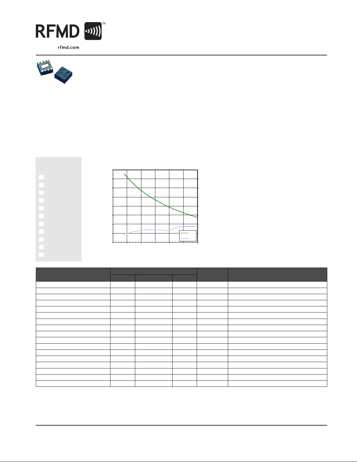
Gain and NF versus Frequency
Broadband Application Circuit (5V, 90mA)
Gain
NF
0.0 0.5 1.0 1.5 2.0 2.5 3.0
Frequency (MHz)
4.00
3.50
3.00
2.50
2.00
1.50
1.00
0.50
0.00
NF (dB)
Features
Ultra-Low Noise Figure=0.60dB
@ 900MHz
Gain=18.9dB @ 900MHz
High Linearity: OIP3=40.5dBm
@ 1900MHz
Channel Power=13.4dBm (-
65dBc IS95 ACPR, 880MHz)
P
=23.4dBm @ 1900MHz
1dB
Single-Supply Operation: 5V @
Idq=90mA
Flexible Biasing Options: 3-5V,
Adjustable Current
Broadband Internal Matching
Applications
Cellular, PCS, W-CDMA, ISM,
WiMAX Receivers
PA Driver Amplifier
Low Noise, High Linearity Gain
Block Applications
Parameter
Min. Typ. Max.
Specification
Unit Condition
Small Signal Power Gain 18.9 dB 0.9GHz
12.9 dB 1.96GHz
Output Power at 1dB Compression 23.0 dBm 0.9GHz
23.4 dBm 1.9GHz
Output Third Order Intercept Point 37.9 dBm 0.9GHz
40.5 dBm 1.9GHz
Noise Figure 0.59 dB 0.9GHz
0.64 dB 1.9GHz
Input Return Loss -14.6 dB 0.9 GHz
-21.0 dB 1.9GHz
Output Return Loss -16.8 dB 0.9GHz
-13.0 dB 1.9GHz
Reverse Isolation -24.1 dB 0.9GHz
-18.4 dB 1.9GHz
Device Operating Voltage 5.00 5.25 V
Device Operating Current 90 mA Quiescent
Thermal Resistance 65 °C/W Junction to lead
Test Conditions: VD=5V, IDQ=90mA, OIP3 Tone Spacing=1MHz, P
Z
=50Ω, 25°C, Broadband Application Circuit
S=ZL
RF MICRO DEVICES®, RFMD®, Optimum Technology Matching®, Enab ling Wireless Connectivity™, PowerStar®, POLARIS™ TOTAL RADIO™ and UltimateBlue™ are trademarks of RFMD, LLC. BLUE TOOTH is a trade-
mark owned by Bluetooth SIG, Inc., U.S.A. and licensed for use by RF MD. All other trade names, trademarks and registered trademarks are the prope rty of their respective owners. ©2006, RF Micro Devices, Inc.
per tone= 0 dBm
OUT
7628 Thorndike Road, Greensboro, NC 27409-9421 · For sales or technical
EDS-105470 Rev E
support, contact RFMD at (+1) 336-678-5570 or sales-support@rfmd.com.
1 of 12
Page 2

SPF-5122Z
Preliminary
Absolute Maximum Ratings
Parameter Rating Unit
Max Device Current (lD)120mA
Max Device Voltage (V
Max RF Input Power 27 dBm
Max Dissipated Power 660 mW
Max Junction Temperature (T
Operating Temperature Range (T
Max Storage Temperature -65 to +150 °C
ESD Rating - Human Body Model
(HBM)
Moisture Sensitivity Level (MSL) MSL 1
Operation of this device beyond any one of these limits may cause permanent
damage. For reliable continuous operation, the device voltage and current
must not exceed the maximum operating values specified in the table on
page one.
Bias Conditions should also satisfy the following expression:
I
<(TJ-TL)/RTH, j-l and TL=T
DVD
)5.5V
D
)150°C
J
) -40 to + 85 °C
L
Class 1B
LEAD
Exceeding any one or a combination of the Absolute Maximum Rating conditions may
cause permanent damage to the device. Extended application of Absolute Maximum
Rating conditions to the device may reduce device reliability. Specified typical performance or functional operation of the device under Absolute Maximum Rating conditions is not implied.
RoHS status based on EUDirective 2002/95/EC (at time of this docume nt revision).
The information in this publication is believed to be accurate and reliable. However, no
responsibility is assumed by RF Micro Devices, Inc. ("RFMD") for its u se, nor for any
infringement of patents, or other rights of third par ties, resulting from its use. No
license is granted by implication or otherwise under any patent or patent rights of
RFMD. RFMD reserves the right to change component circuitry, recommended application circuitry and specifications at any time without prior notice.
Caution! ESD sensitive device.
Typical RF Performance - Broadband Application Circuit with VD=5V, ID=90mA
Parameter Unit 0.1
GHz*
Small Signal Gain dB 27.0 24.0 19.0 15.0 13.0 12.0 11.0 6.0 7.0
Noise Figure dB 0.42 0.47 0.59 0.70 0.64 0.73 0.86 1.35 1.27
Output IP3 dBm 33.0 36.0 38.0 39.5 40.5 41.0 41.5 40.5 41.5
Output P1dB dBm 22.3 22.7 23.0 23.2 23.4 23.7 23.9 22.2 22.9
Input Return Loss dB -9.5 -10.0 -14.5 -20.0 -21.0 -22.0 -22.5 -15.0 -11.5
Output Return Loss dB -29.0 -19.5 -17.0 -14.0 -13.0 -12.5 -12.5 -7.5 -15.5
Reverse Isolation dB -32.0 -29.0 -24.0 -20.0 -18.5 -17.5 -16.5 -15.5 -13.5
Test Conditions: VD=5V, IDQ=90mA, OIP3 Tone Spacing= 1 MHz, P
1. Input RL can be improved in the 800MHz to 1000MHz band by adding a series inductor between the DC block and device input.
0.4
GHz
0.9
GHz
1.5
GHz
per tone=0 dBm, TL=25°C, ZS=ZL=50Ω, *Bias Tee Data @ 100 MHz
OUT
1.9
GHz
2.2
GHz
2.5
GHz
3.5
GHz
Typical RF Performance - Broadband Application Circuit with VD=3V, ID=58mA
Parameter Unit 0.1
GHz*
Small Signal Gain dB 26.0 23.0 18.5 14.5 12.5 11.5 10.5 6.0 6.5
Noise Figure dB 0.35 0.44 0.58 0.65 0.61 0.69 0.79 1.25 1.19
Output IP3 dBm 31.5 33.0 34.5 36.0 36.5 37.0 37.5 37.0 37.5
Output P1dB dBm 18.8 18.9 19.1 19.4 19.9 20.2 20.1 18.9 19.2
Input Return Loss dB -8.0 -9.0 -13.0 -16.5 -18.5 -19.0 -19.0 -13.5 -10.0
Output Return Loss dB -26.0 -28.5 -23.5 -18.0 -16.5 -16.0 -15.5 -9.0 -14.0
Reverse Isolation dB -31.0 -28.0 -23.0 -19.0 -17.5 -16.0 -15.0 -14.5 -12.5
Test Conditions: VD=3V, IDQ=58mA, OIP3 Tone Spacing= 1 MHz, P
1. Input RL can be improved in the 800MHz to 1000MHz band by adding a series inductor between the DC block and device input.
0.4
GHz
0.9
GHz
1.5
GHz
per tone=0 dBm, TL=25°C, ZS=ZL=50Ω, *Bias Tee Data @ 100MHz
OUT
1.9
GHz
2.2
GHz
2.5
GHz
3.5
GHz
3.8
GHz
3.8
GHz
2 of 12
7628 Thorndike Road, Greensboro, NC 27409-9421 · For sales or technical
support, contact RFMD at (+1) 336-678-5570 or sales-support@rfmd.com.
EDS-105470 Rev E
Page 3

Preliminary
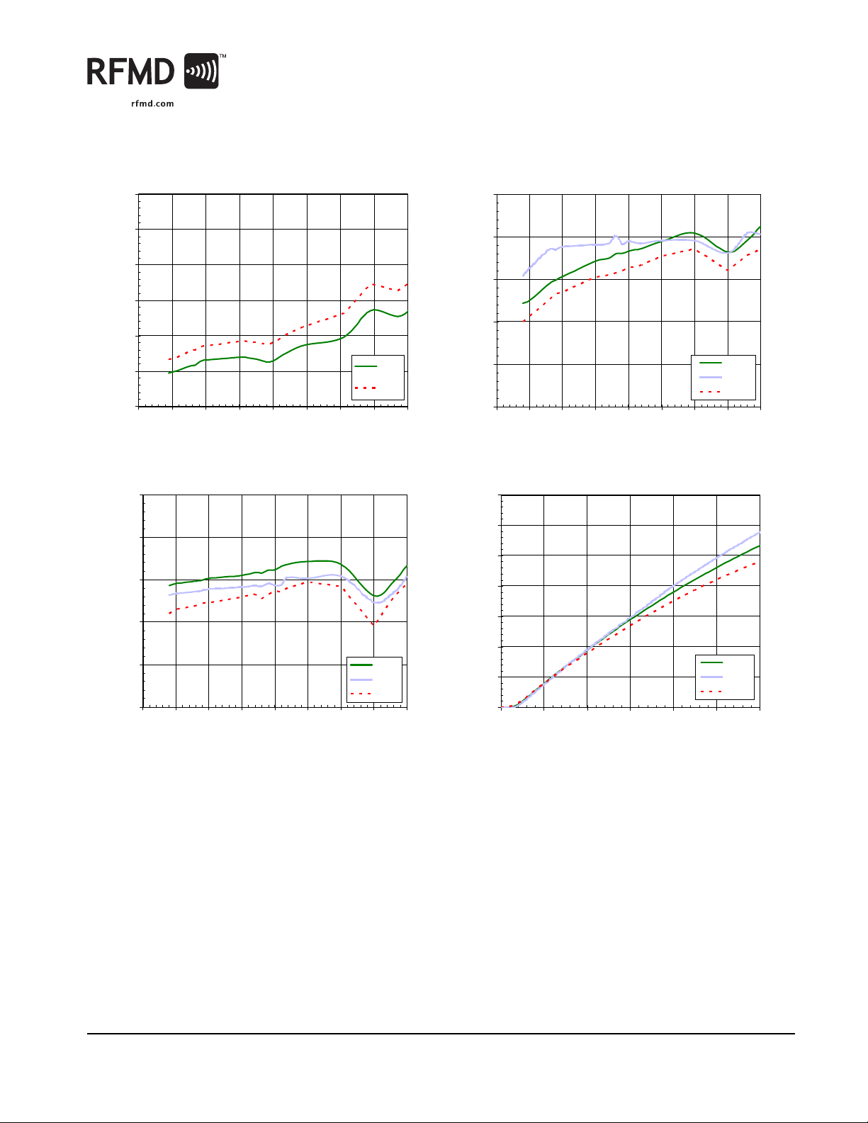
Typical RF Performance - Broadband Application Circuit with VD=5V, ID=90mA
SPF-5122Z
NF versus Frequency
3.0
2.5
2.0
1.5
NF (dB)
1.0
0.5
0.0
0.0 0.5 1.0 1.5 2.0 2.5 3.0 3.5 4.0
Frequency (GHz)
P
versus Frequency
1dB
27.0
25.0
25°C
85°C
OIP3 versus Frequency
46.0
42.0
38.0
(dBm)
3
34.0
OIP
30.0
26.0
0.0 0.5 1.0 1.5 2.0 2.5 3.0 3.5 4.0
(0 dBm/tone, 1 MHz spacing)
Frequency (GHz)
Device Current versus Voltage
140.0
120.0
100.0
25°C
-40°C
85°C
23.0
(dBm)
1dB
21.0
P
19.0
17.0
0.0 0.5 1.0 1.5 2.0 2.5 3.0 3.5 4.0
Frequency (GHz)
25°C
-40°C
85°C
80.0
(mA)
D
I
60.0
40.0
20.0
0.0
0.0 1.0 2.0 3.0 4.0 5.0 6.0
VD (V)
25°C
-40°C
85°C
EDS-105470 Rev E
7628 Thorndike Road, Greensboro, NC 27409-9421 · For sales or technical
support, contact RFMD at (+1) 336-678-5570 or sales-support@rfmd.com.
3 of 12
Page 4

SPF-5122Z
Preliminary
Typical RF Performance - Broadband Application Circuit with VD=5V, ID=90mA
S11 versus Frequency
0.0
-5.0
-10.0
-15.0
S11 (dB)
-20.0
-25.0
-30.0
0.0 0.5 1.0 1.5 2.0 2.5 3.0 3.5 4.0
Frequency (GHz)
S12 versus Frequency
0.0
-5.0
-10.0
25°C
-40°C
85°C
S21 versus Frequency
32.0
28.0
24.0
20.0
16.0
S21 (dB)
12.0
8.0
4.0
0.0
0.0 0.5 1.0 1.5 2.0 2.5 3.0 3.5 4.0
Frequency (GHz)
S22 versus Frequency
0.0
-5.0
-10.0
25°C
-40°C
85°C
-15.0
S12 (dB)
-20.0
-25.0
-30.0
0.0 0.5 1.0 1.5 2.0 2.5 3. 0 3. 5 4.0
Frequency (GHz)
25°C
-40°C
85°C
-15.0
S22 (dB)
-20.0
-25.0
-30.0
0.0 0.5 1.0 1.5 2.0 2.5 3.0 3.5 4.0
Frequency (GHz)
25°C
-40°C
85°C
4 of 12
7628 Thorndike Road, Greensboro, NC 27409-9421 · For sales or technical
support, contact RFMD at (+1) 336-678-5570 or sales-support@rfmd.com.
EDS-105470 Rev E
Page 5

Preliminary
Typical RF Performance - Broadband Application Circuit with VD=5V, ID=90mA
SPF-5122Z
OIP3 versus Power
46.0
42.0
38.0
(dBm)
3
34.0
OIP
30.0
26.0
0.0 3.0 6.0 9.0 12.0 15.0
(900 MHz, 1 MHz spacing)
Output Power per Tone (dBm)
ACP versus Channel Power @ 880MHz
-30.0
-40.0
-50.0
-60.0
IS-95 with 9 DPCH
ACP (dBc)
-70.0
25°C
-40°C
85°C
880MHz IS95 Source
-40°C
25°C
85°C
OIP3 versus Power
46.0
42.0
38.0
(dBm)
3
34.0
OIP
30.0
26.0
0.0 3.0 6.0 9.0 12.0 15.0
(1900 MHz, 1 MHz spacing)
Output Power per Tone (dBm)
ACP versus Channel Power @ 2140MHz
-30.0
-40.0
-50.0
-60.0
ACP (dBc)
WCDMA w ith 64 DPCH
25°C
-40°C
85°C
-40°C
25°C
85°C
System
-80.0
-90.0
0.0 2.0 4.0 6.0 8.0 10.0 12.0 14.0 16.0 18.0
EDS-105470 Rev E
-70.0
Source
-80.0
5.0 7.0 9.0 11.0 13.0 15.0 17.0
Channel Power (dBm)
7628 Thorndike Road, Greensboro, NC 27409-9421 · For sales or technical
support, contact RFMD at (+1) 336-678-5570 or sales-support@rfmd.com.
Source
Channel Power (dBm)
5 of 12
Page 6

SPF-5122Z
Preliminary
Typical RF Performance - Broadband Application Circuit with VD=3V, ID=58mA
NF versus Frequency
3.0
2.5
2.0
1.5
NF (dB)
1.0
0.5
0.0
0.0 0.5 1.0 1.5 2.0 2.5 3.0 3.5 4.0
Frequency (GHz)
P
versus Frequency
1dB
22.0
20.0
25°C
85°C
OIP3 versus Frequency
42.0
38.0
34.0
(dBm)
3
30.0
OIP
26.0
22.0
0.0 0.5 1.0 1.5 2.0 2.5 3.0 3.5 4.0
(0 dBm/tone, 1 MHz spacing)
Frequency (GHz)
25°C
-40°C
85°C
18.0
(dBm)
1dB
16.0
P
14.0
12.0
0.0 0.5 1.0 1.5 2.0 2.5 3.0 3.5 4.0
Frequency (GHz)
25°C
-40°C
85°C
6 of 12
7628 Thorndike Road, Greensboro, NC 27409-9421 · For sales or technical
support, contact RFMD at (+1) 336-678-5570 or sales-support@rfmd.com.
EDS-105470 Rev E
Page 7

SPF-5122Z
Preliminary
Typical RF Performance - Broadband Application Circuit with VD=3V, ID=58mA
S11 versus Frequency
0.0
-5.0
-10.0
-15.0
S11 (dB)
-20.0
-25.0
-30.0
0.0 0.5 1.0 1.5 2.0 2.5 3.0 3.5 4.0
Frequency (GHz)
S12 versus Frequency
0.0
-5.0
-10.0
25°C
-40°C
85°C
S21 versus Frequency
32.0
28.0
24.0
20.0
16.0
S21 (dB)
12.0
8.0
4.0
0.0
0.0 0.5 1.0 1.5 2.0 2.5 3.0 3.5 4.0
Frequency (GHz)
S22 versus Frequency
0.0
-5.0
-10.0
25°C
-40°C
85°C
-15.0
S12 (dB)
-20.0
-25.0
-30.0
0.0 0.5 1.0 1.5 2.0 2.5 3.0 3.5 4.0
Frequency (GHz)
25°C
-40°C
85°C
-15.0
S22 (dB)
-20.0
-25.0
-30.0
0.0 0.5 1.0 1.5 2.0 2.5 3.0 3.5 4.0
Frequency (GHz)
25°C
-40°C
85°C
7 of 12
7628 Thorndike Road, Greensboro, NC 27409-9421 · For sales or technical
support, contact RFMD at (+1) 336-678-5570 or sales-support@rfmd.com.
EDS-105470 Rev E
Page 8

SPF-5122Z
0.0
0.2
1.0
2.0
5.0
0.2
0.5
1.0
2.0
5.0
0.2
0.5
1.0
2.0
5.0
z
z
z
50 MHz
z
z
z
8 GHz
0.5 GHz
0.0
0.2
0.5
2.0
5.0
0.2
0.5
1.0
2.0
5.0
0.2
0.5
1.0
2.0
5.0
z
z
z
50 MHz
3 GHz
8
z
0.5 GHz
z
Preliminary
De-embedded Device S-parameters (Bias Tee Data)
G
versus Frequency
MAX
30.0
(5V, 90mA)
Gmax
25.0
20.0
15.0
, Gain (dB)
MAX
G
10.0
5.0
0.0
0.0 1.0 2.0 3.0 4.0 5.0 6.0 7.0 8.0
Gain
Frequency (GHz)
S11 versus Frequency (5V 46mA) S22 versus Frequency (5V 46mA)
3 GH
2 GH
4 GH
1 GH
6 GH
6 GH
GH
1 GH
2 GH
4 GH
7628 Thorndike Road, Greensboro, NC 27409-9421 · For sales or technical
8 of 12
support, contact RFMD at (+1) 336-678-5570 or sales-support@rfmd.com.
EDS-105470 Rev E
Page 9

Preliminary
0.0
0.2
1.0
2.0
5.0
0.2
0.5
1.0
2.0
5.0
0.2
0.5
1.0
2.0
5.0
z
2 GHz
z
50 MHz
z
z
z
z
0.0
0.2
0.5
2.0
5.0
0.2
0.5
1.0
2.0
5.0
0.2
0.5
1.0
2.0
5.0
4
z
2 GHz
z
z
8 GHz
z
G
MAX
30.0
versus Frequency
(3V, 58mA)
SPF-5122Z
Gmax
25.0
20.0
15.0
Gain
, Gain (dB)
MAX
G
10.0
5.0
0.0
0.0 1.0 2.0 3.0 4.0 5.0 6.0 7.0 8.0
Frequency (GHz)
S11 versus Frequency (3V 25mA) S22 versus Frequency (3V 25mA)
3 GH
4 GH
1 GH
6 GH
0.5 GH
8 GH
6 GH
0.5 GH
1 GH
GH
7628 Thorndike Road, Greensboro, NC 27409-9421 · For sales or technical
EDS-105470 Rev E
support, contact RFMD at (+1) 336-678-5570 or sales-support@rfmd.com.
9 of 12
Page 10

SPF-5122Z
out
s
H
F
F
Z
d
F
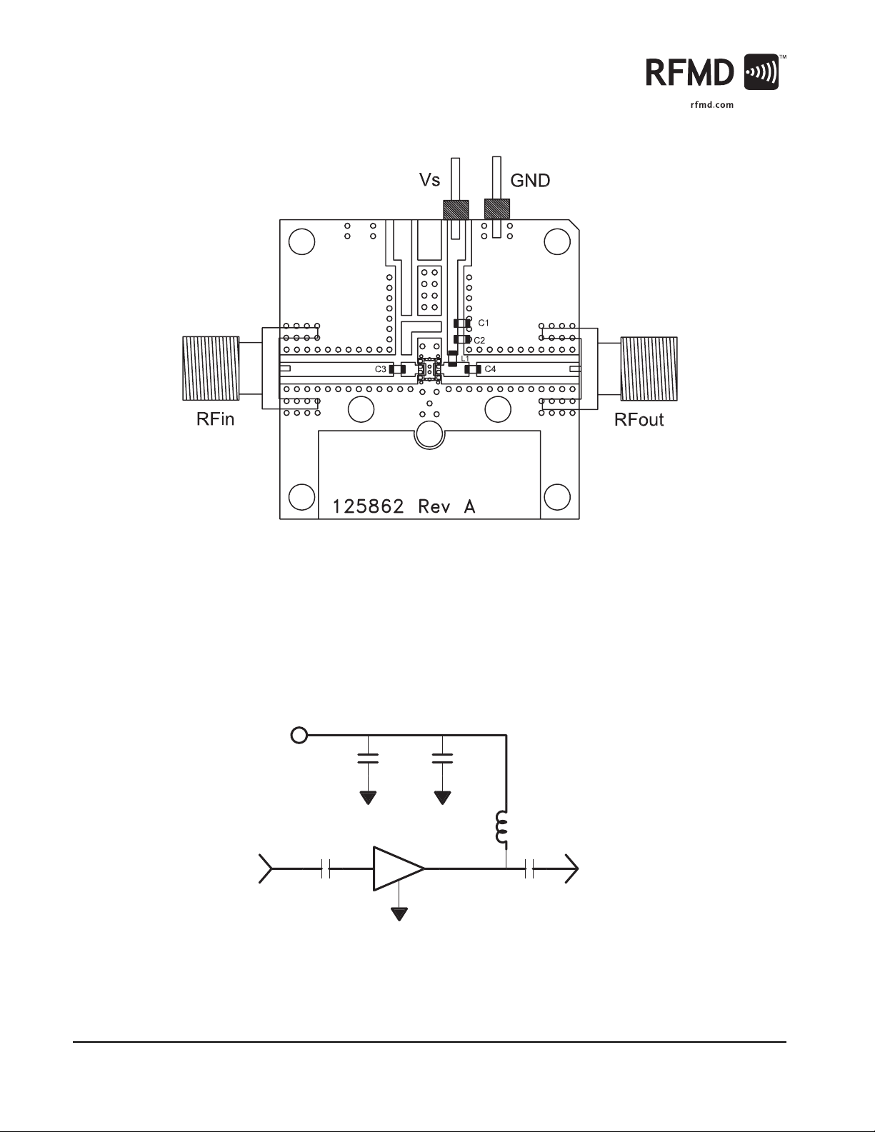
Evaluation Board Layout and Bill of Materials
Preliminary
Bill of Materials (SPF-5122Z, 400MHz to 3000 MHz
C1 TAJB104KLRH, Rohm, 0.1uF
C2 MCH185A101JK, Rohm, 100pF
C3 MCH185A101JK, Rohm, 100pF
C4 MCH185A101JK, Rohm, 100pF
L1 LL1608-FSR15J, Toko, 150nH
PCB 125862-A
Application Schematic
(400MHz to 3000MHz)
V
.1u
100p
100p
150n
PF-5122
100pF
Epa
F
7628 Thorndike Road, Greensboro, NC 27409-9421 · For sales or technical
10 of 12
support, contact RFMD at (+1) 336-678-5570 or sales-support@rfmd.com.
EDS-105470 Rev E
Page 11

Preliminary
Z
F
)
0057
0088
95
00
0337
SPF-5122Z
Pin Function Description
1,3,5,
N/A
Ground or No-Connect. No connection internal
6,8
2RF IN
4N/A
7RF OUT/BIAS
EPAD GND
RF Input, DC coupled and matched to 50Ω. An external DC block is required.
Ground or No-Connect. Internally Grounded.
RF Output, Bias applied through this pin. Matched to 50Ω.
EPAD must be conductively attached to RF and DC ground.
Part Identification Suggested Pad Layout
Pin 1 Designation (top view
.02
.
P
1
.
Package Drawing
Dimensions in inches (millimeters)
Refer to drawing posted at www.rfmd.com for tolerances.
.
.02
Ordering Information
Part Number Description Reel Size Devices/Reel
SPF-5122Z Lead Free, RoHS Compliant 7” 3000
SPF-5122Z-EVB1 400 MHz to 3000MHz Evaluation Board N/A N/A
7628 Thorndike Road, Greensboro, NC 27409-9421 · For sales or technical
EDS-105470 Rev E
support, contact RFMD at (+1) 336-678-5570 or sales-support@rfmd.com.
11 of 12
Page 12

SPF-5122Z
Preliminary
12 of 12
7628 Thorndike Road, Greensboro, NC 27409-9421 · For sales or technical
support, contact RFMD at (+1) 336-678-5570 or sales-support@rfmd.com.
EDS-105470 Rev E
 Loading...