

Page 1
HIGH-CURRENT MOTOR CONTROLLER/DRIVER
1
OUT
A
CLOCK
OUT
SENSE
SENSE
OUT
CLOCK
OUT
2
A
3
A
4
A
5
A
6
A
7
A
8
A
9
A
10
B
11 12
B
B
13
B
14
B
15
B
16
B
17
B
18
B
STROBE
REF/ENABLE
CNTRL SPLY
SERIAL DATA
GROUND
GROUND
STROBE
REF/ENABLE
CNTRL SPLY
SERIAL DATA
ABSOLUTE MAXIMUM RATINGS
Load Supply Voltage, VBB. . . . . . . . . . . . 46 V
FET Output Voltage, V
Control Supply Voltage, V
Peak Output Current,
I
(t
≤ 10 µs). . . . . . . . . . . . . . . . 5.0 A
OUTM
Continuous Output Current, I
SLA7042M . . . . . . . . . . . . . . . . . . . . . 1.5 A
SLA7044M . . . . . . . . . . . . . . . . . . . . . 3.0 A
Input Voltage Range,
V
IN
Reference Voltage, V
Package Power Dissipation, PD. See Graph
Junction Temperature, T
Operating Temperature Range,
T
A
Storage Temperature Range,
T
stg
w
. . . . . . . . . . . . . . -0.3 V to VDD + 0.3 V
. . . . . . . . . . . . . . . . . . . . -20°C to +85°C
. . . . . . . . . . . . . . . . . . -40°C to +150°C
at T
SR/LATCH
V
REF
V
CC
V
REF
V
CC
SR/LATCH
= +25°C
A
DS
REF
ø
CONTROL/LOGIC
D/A
+
+
CONTROL/LOGIC
D/A
ø
. . . . . . . . . . . 100 V
. . . . . . . . . 7.0 V
DD
OUT
. . . . . . . . . . . . V
. . . . . . . . . +150°C
J
Dwg. PK-008
DD
SLA7042M
AND
SLA7044M
MICROSTEPPING, UNIPOLAR PWM,
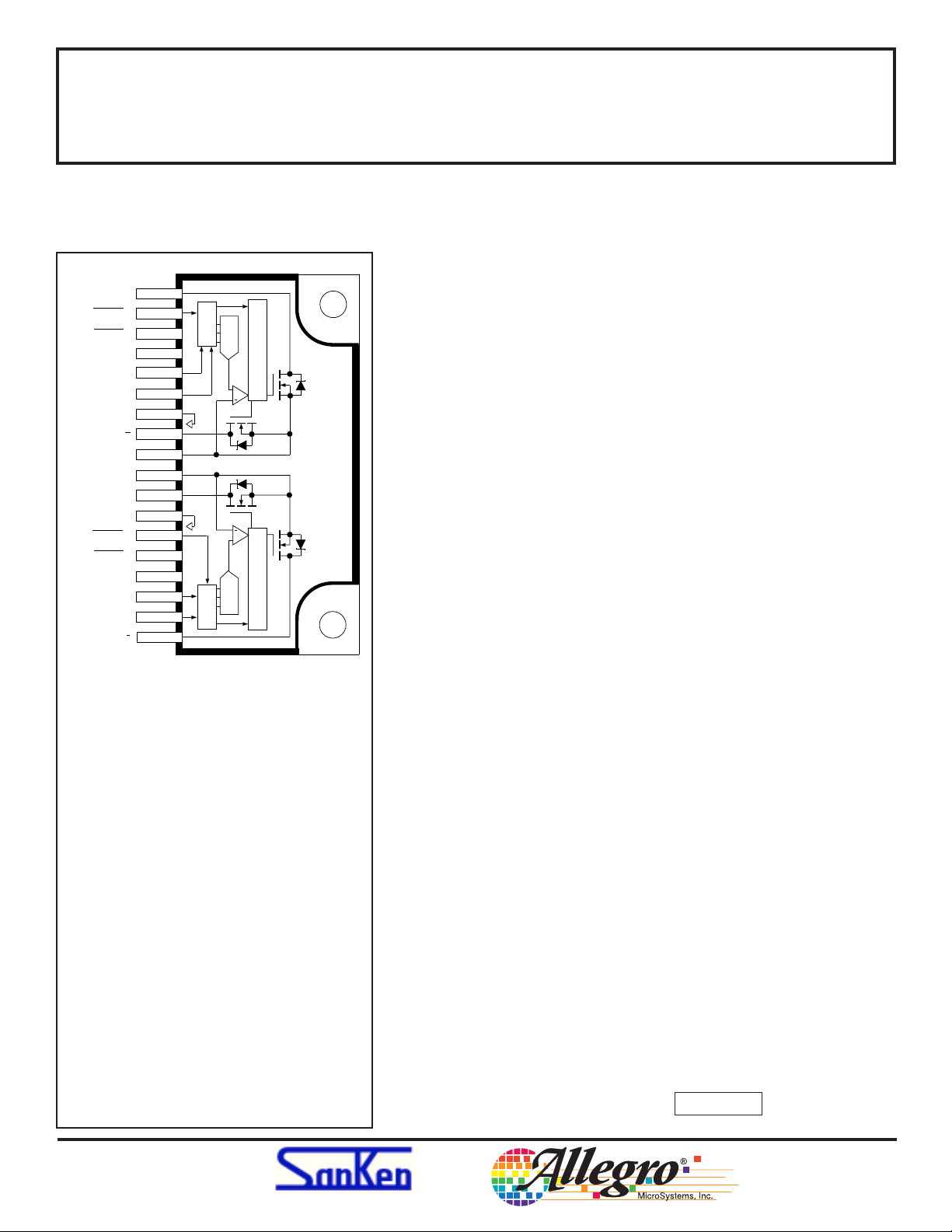
The SLA7042M and SLA7044M are designed for high-efficiency
and high-performance microstepping operation of 2-phase, unipolar
stepper motors. Microstepping provides improved resolution without
limiting step rates, and provides much smoother low-speed motor
operation. An automated, innovative packaging technology combined
with power NMOS FETs and monolithic CMOS logic/control circuitry
advances power multi-chip modules (PMCMs™) toward the complete
integration of motion control. Each half of these stepper motor controller/drivers operate independently. The 4-bit shift registers are serially
loaded with motor phase information and output current-ratio data (eight
levels). The combination of user-selectable current-sensing resistor,
linearly adjustable reference voltage, and digitally selected output
current ratio provides users with a broad, variable range of of full, half,
and microstepping motor control (I
Each PMCM is rated for a maximum motor supply voltage of 46 V
and utilizes advanced NMOS FETs for the high-current, high-voltage
driver outputs. The avalanche-rated (≥100 V) FETs provide excellent
ON resistance, improved body diodes, and very-fast switching. The
multi-chip ratings and performance afford significant benefits and
advantages for stepper drives when compared to the higher dissipation
and slower switching speeds associated with bipolar transistors. Highly
automated manufacturing techniques provide low-cost and exceptionally reliable PMCMs suitable for controlling and directly driving a broad
range of 2-phase, unipolar stepper motors. The SLA7042M and
SLA7044M are identical except for
Complete applications information is given on the following pages.
PWM current is regulated by appropriately choosing current-sensing
resistors, a voltage reference, and digitally programmable current ratio.
Inputs are compatible with 5 V logic and microprocessors.
BENEFITS AND FEATURES
■ Cost-Effective, Multi-Chip Solution
■ ‘Turn-Key’ Motion-Control Module
■ Motor Operation to 3 A and 46 V
■ 3rd Generation High-Voltage FETs
■ 100 V, Avalanche-Rated NMOS
■ Low r
■ Advanced, Improved Body Diodes
■ Microstepping Unipolar Drive
■ High-Efficiency, High-Speed PWM
Always order by complete part number: SLA7042M .
NMOS Outputs
DS(on)
OUT
r
DS(on)
≈ [V
/3 • RS] • Current Ratio).
REF
and output current ratings.
■ Independent PWM Current Control
(2-Phase)
■ Digitally Programmable PWM
Current Control
■ Low Component-Count PWM Drive
■ Low Internal-Power Dissipation
■ Electrically Isolated Power Tab
■ Logic IC- and µP-Compatible
Inputs
■ Machine-Insertable Package
Data Sheet
28202A*
™
Page 2
SLA7042M
2
5
0
8
7
AND
SLA7044M
MICROSTEPPING,
UNIPOLAR PWM, HIGH-CURRENT
MOTOR CONTROLLER/DRIVERS
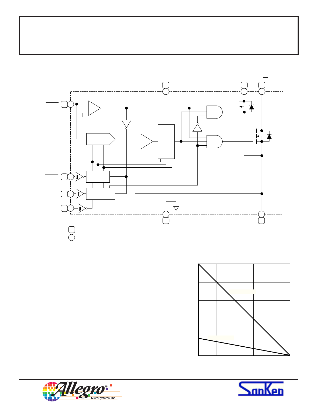
FUNCTIONAL BLOCK DIAGRAM
REF/ENABLE
STROBE
DATA
CLOCK
CONTROL
SUPPLY
4 8
1
V
DD
143
+
V – 1
DD
V
REF
132
1
6
165
CHANNEL A PIN NUMBERS
CHANNEL B PIN NUMBERS
D/A
LATCHES
SHIFT REG
ENABLE
+
NOISE FILTER
PWM OFF TIMER
PROGRAMMABLE
PHASE
1
7
GROUND
OUT
OUT
A/B
1
11
A/B
1
1
9
SENSE
Dwg. FK-006
Note that channels A and B are electrically isolated.
ALLOWABLE PACKAGE
POWER DISSIPATION
115 Northeast Cutoff, Box 15036
Worcester, Massachusetts 01615-0036 (508) 853-5000
Copyright © 1995, 1998 Allegro MicroSystems, Inc.
25
20
R = 5.0°C/W
θJM
15
10
5
R = 28°C/W
θJA
0
25
ALLOWABLE PACKAGE POWER DISSIPATION in WATTS
50 75 100 125 150
TEMPERATURE in °C
Dwg. GK-018-1
™
Page 3
SLA7042M
AND
SLA7044M
MICROSTEPPING,
UNIPOLAR PWM, HIGH-CURRENT
MOTOR CONTROLLER/DRIVERS
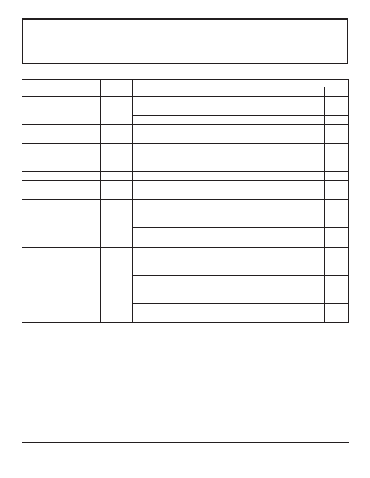
DC ELECTRICAL CHARACTERISTICS at T
= +25°C, V
A
= 5 V unless otherwise noted.
DD
Limits
Characteristic Symbol Test Conditions Min Typ Max Units
FET Leakage Current I
FET ON Voltage V
FET ON Resistance r
Body Diode Forward Voltage V
Control Supply Voltage V
Control Supply Current I
Logic Input Voltage V
V
Logic Input Current I
REF/ENABLE Input Voltage V
DSS
DS(ON)
DS(on)
SD
DD
DD
IN(1)
IN(0)
IN(1)
I
IN(0)
REF/EN
VDS = 100 V — — 4.0 mA
SLA7042M, I
SLA7044M, I
SLA7042M, I
SLA7044M, I
SLA7042M, I
SLA7044M, I
= 1.2 A — — 800 mV
OUT
= 3 A — — 855 mV
OUT
= 1.2 A — — 0.67 Ω
OUT
= 3 A — — 0.285 Ω
OUT
= –1.2 A — — 1.2 V
OUT
= –3 A — — 1.6 V
OUT
Operating 4.5 5.0 5.5 V
Each controller, VDD = 5.5 V — — 7.0 mA
3.5 — — V
— — 1.5 V
V
= V
IN(1)
DD
V
= 0 — — –1.0 µA
IN(0)
— — 1.0 µA
DATA, CLOCK, STROBE, and OUT Enabled 0.4 — 2.5 V
DATA, CLOCK, STROBE, and OUT Disabled VDD - 1 — — V
REF/ENABLE Input Current I
REF/EN
0 V ≤ V
≤ 5 V — — ±1.0 µA
REF/EN
Step Reference SRCR DATA Input = 000X — 0 — %
Current Ratio DATA Input = 001X — 20 — %
DATA Input = 010X — 40 — %
DATA Input = 011X — 55.5 — %
First Bit Entered (X) = Phase DATA Input = 100X — 71.4 — %
Second Bit Entered = LSB DATA Input = 101X — 83 — %
Last Bit Entered = MSB DATA Input = 110X — 91 — %
DATA Input = 111X — 100 — %
NOTE: Negative current is defined as coming out of (sourcing) the specified device pin.
TYPICAL AC CHARACTERISTICS at T
= +25°C, V
A
= 5 V, I
DD
= 1 A, Logic Levels are VDD and
OUT
Ground
PWM OFF Time DATA Input = 001X ................................................................. 7 µs
DATA Input = 010X ................................................................. 7 µs
DATA Input = 011X ................................................................. 9 µs
DATA Input = 100X ................................................................. 9 µs
DATA Input = 101X ................................................................. 9 µs
DATA Input = 110X ................................................................ 11 µs
DATA Input = 101X ................................................................ 11 µs
Output RiseTime t
Output Fall Time t
Strobe-to-Output Switching Time t
r
f
pd
10% to 90% ........................................................................... 0.5 µs
90% to 10% ........................................................................... 0.1 µs
50% to 50% ........................................................................... 0.7 µs
Page 4

SLA7042M
AND
SLA7044M
MICROSTEPPING,
UNIPOLAR PWM, HIGH-CURRENT
MOTOR CONTROLLER/DRIVERS
CLOCK
DATA
STROBE
D
B
A
C
D
E
A
B
C
F
Dwg. WK-002
SERIAL PORT TIMING CONDITIONS
(T
= +25°C, Logic Levels are V
A
A. Minimum Data Active Time Before Clock Falling Edge (Data Set-Up Time) ........... 150 ns
B. Minimum Data Active Time After Clock Falling Edge (Data Hold Time) .................. 150 ns
C. Minimum Data Pulse Width...................................................................................... 350 ns
D. Minimum Clock Pulse Width .................................................................................... 350 ns
E. Minimum Time Between Clock and Strobe Falling Edges ....................................... 650 ns
F. Minimum Strobe Pulse Width ................................................................................... 500 ns
and Ground)
DD
APPLICATIONS INFORMATION
The SLA7042M and SLA7044M modules integrate two
CMOS controller ICs and four NMOS FETs. Each half of the
device operates independently, although the CLOCK inputs
may be connected together and the STROBE inputs may be
connected together. Pulling V
bit shift registers to be serially loaded with motor phase and
output currrent ratioing data.
The first bit selects the motor phase (logic high = Output A
or B, logic low = Output A or B); the next three bits determine
the motor current ratio (eight steps, 0% to 100%). The internal
D/A converter, in conjunction with a current-sensing resistor
and input reference voltage, completes the microstepping
current control.
Pulling V
high (within 1 V of VDD) resets the shift
REF/EN
register and latches to turn the MOS drivers OFF and inhibits
the serial DATA input.
115 Northeast Cutoff, Box 15036
Worcester, Massachusetts 01615-0036 (508) 853-5000
low (<2.5 V) allows the 4-
REF/EN
™
Page 5

SLA7042M
AND
SLA7044M
MICROSTEPPING,
UNIPOLAR PWM, HIGH-CURRENT
MOTOR CONTROLLER/DRIVERS
REGULATING THE PWM OUTPUT CURRENT
The output current (and motor coil current) waveform
is illustrated in Figure 1. Setting the maximum PWM
current trip point to meet the specified full-step running
current for the motor, I
100% ratio), requires only a current-sensing resistor, RS,
and an input reference voltage, V
and 2.5 V.
I
OUT
PHASE A
0
PHASE A
FIGURE 1.␣ PHASE A COIL CURRENT WAVEFORM
max (DATA input = 111X =
OUT
, between 0.4 V
REF/EN
V
max ≈
REF/EN
3 • R
S
I
OUT
Dwg. WK-001
SERIAL DATA INPUT ENABLE
In a minimum-component application, a voltage divider
provides V
and an npn transistor provides the
REF/EN
required pull-down to enable the serial data input as
shown in Figure 2.
I
OUT
max ≈
R
2
R1 + R
2
V
3 • R
b
S
•
µP STEPPER MOTOR CONTROL
Alternative REFERENCE/ENABLE input configurations provide for more complete motor control. A tri-state
logic element and a voltage divider allows a fixed reference voltage, with both output disable and data enable
functions. Complete µP control is usually accomplished
with a D/A converter as shown in Figure 3. Here, digital
control provides an output disable (>VDD - 1 V), V
VEN (<2.5 V).
REF
, and
ENABLE
DATA
V
DD
V
b
R
R
TO CHANNEL B
1
V
REF/EN
2
SERIAL DATA
D/A
PWM
OFF-TIME
CONTROL
FIGURE 2.␣ PWM CONTROL (RUN MODE)
Ø
CONTROL
LOGIC
V
BB
AA
DRIVE
SENSE
R
S
Dwg. EK-011
B
B
Page 6

SLA7042M
AND
SLA7044M
MICROSTEPPING,
UNIPOLAR PWM, HIGH-CURRENT
MOTOR CONTROLLER/DRIVERS
V
b
R
1
R
H = OFF
Z = REFERENCE
L = ENABLE DATA
2
FIGURE 3. ␣COMPLETE CONTROL
SERIAL DATA INPUT
The serial DATA input port is enabled (active low) by
the REFERENCE/ENABLE input. When V
tween 0.4 V and 2.5 V, information on the DATA input is
read into the shift register on each high-to-low transition of
the CLOCK.
There are four bits: the first bit entered controls the
REF/EN
is be-
V
DD
TO OTHER CHANNEL
D/A
V
REF/EN
(OPTIONAL)
......
FROM µP
111...1 = OFF
000...0 = ENABLE DATA
Dwg. EK-012
motor phase — a high level enables OUTA or OUTB, a low
level enables OUTA or OUTB. The next three bits set the
step reference voltage ratio and PWM OFF time as shown
in the Characteristics Tables — the least-significant bit first
and the most-significant bit last.
Data written into the serial data port is latched and
becomes active on a high-to-low transition at STROBE.
LOAD CURRENT
(NOT TO SCALE)
V
DD
- 1 V
REFERENCE/ENABLE
2.5 V
CLOCK
SERIAL DATA
STROBE
DISABLED
0
V
DD
MOTOR PWM OPERATION
ENTER
0
DD
V
0
V
DD
0
V
DD
0
DATA
3.1 µs
MIN
0 0 1 0
= 20%
DATA LATCHED
DON'T CARE
0 1 0 0
= 40%
Dwg. WK-003
FIGURE 4. ␣TIMING RELATIONSHIPS
115 Northeast Cutoff, Box 15036
Worcester, Massachusetts 01615-0036 (508) 853-5000
™
Page 7

SLA7042M
AND
SLA7044M
MICROSTEPPING,
UNIPOLAR PWM, HIGH-CURRENT
MOTOR CONTROLLER/DRIVERS
REFERENCE/ENABLE INPUT
The serial DATA input port is enabled (active low) by
the REFERENCE/ENABLE input when V
0.4 V and 2.5 V. With V
greater than VDD - 1 V, the
REF/EN
REF/EN
is between
serial DATA input port is disabled, the outputs are OFF,
and the controller/driver will not be affected by changes at
the DATA, CLOCK, or STROBE inputs.
With V
current limit is a linear function of V
between 0.4 V and 2.5 V, the output
REF/EN
and the step
REF
reference current ratio.
V
≈
REF
3 • R
• SRCR
S
I
OUT
In a typical (SLA7042M) application where VDD = 5 V,
a V
allowable load current of 1.2 A, the maximum value of R
is 0.69 Ω and I
between 0.4 V and 2.5 V, and a maximum
REF/EN
min is 0.11 A when SRCR is 100%
OUT
S
(DATA input = 111X).
POWER DISSIPATION CALCULATIONS
The SLA7042/44M normally do not require special
heat sinking except under unusual circumstances (two
phases operating near maximum output current and T
A
>65°C). However, as with all power drivers, the basic
constituents of power dissipation should be evaluated.
Conduction losses (internal power dissipation) include:
(a) FET output power dissipation (I
I
OUT
• V
DS(ON)
),
(b) FET body diode power dissipation (VSD • I
OUT
2
• r
DS(on)
or
OUT
), and
(c) control circuit power dissipation (VDD • IDD).
PACKAGE RATINGS/DERATING FACTORS
Thermal calculations must also consider the temperature effects on the output FET ON resistance. The applicable thermal ratings for the 18-lead power-tab SIP PMCM
package are:
R
= 28°C/W (junction to ambient with no heat sink)
θJA
or 4.5 W at +25°C and a derating factor of -36 mW/°C
for operation above +25°C.
R
= 5°C/W (junction to mounting surface).
θJM
TEMPERATURE EFFECTS ON FET r
DS(on)
Analyzing safe, reliable operation includes a concern
for the relationship of NMOS ON resistance to junction
temperature. Device package power calculations must
include the increase in ON resistance (producing higher
output ON voltages) caused by higher operating junction
temperatures. Figure 5 provides a normalized ON resistance curve, and all thermal calculations should consider
increases from the given +25°C limits, which may be
caused by internal heating during normal operation.
2.5
2.0
1.5
1.0
0.5
NORMALIZED FET ON RESISTANCE
0
-40 +80 +160
0
JUNCTION TEMPERATURE in °C
+40 +120
Dwg. GK-017
FIGURE 5.␣ NORMALIZED ON RESISTANCE
vs TEMPERATURE
The power MOSFET outputs of these devices are
similar to the International Rectifier type IRL510
(SLA7042M) and IRL520 (SLA7044M). These devices
feature an excellent combination of fast switching, ruggedized device design, low on-resistance, and cost effectiveness.
Page 8

SLA7042M
AND
SLA7044M
MICROSTEPPING,
UNIPOLAR PWM, HIGH-CURRENT
MOTOR CONTROLLER/DRIVERS
Dimensions in Inches
(for reference only)
1.22
±0.008
0.126
±0.006
ø
0.630
±0.008
118
0.026
0.961
0.646
±0.008
1.232
+0.008
–0.004
±0.008
±0.008
0.126
0.390
0.022
0.066
±0.016
±0.006
0.189
±0.008
±0.008
0.512
±0.008
0.264
±0.020
+0.008
–0.004
x 0.150
0.067
±0.004
0.096
±0.008
0.118
0.157
±0.028
Dimensions in Millimeters
(controlling dimensions)
31
±0.2
3.2
ø
±0.15
±0.2
16
118
The products described here are manufactured in Japan by Sanken Electric Co.,
Ltd. for sale by Allegro MicroSystems, Inc.
Sanken Electric Co., Ltd. and Allegro MicroSystems, Inc. reserve the right to
make, from time to time, such departures from the detail specifications as may be
required to permit improvements in the design of their products.
The information included herein is believed to be accurate and reliable.
However, Sanken Electric Co., Ltd. and Allegro MicroSystems, Inc. assume no
responsibility for its use; nor for any infringements of patents or other rights of third
parties which may result from its use.
0.65
24.4
16.4
31.3
+0.2
–0.1
±0.2
±0.2
±0.2
Dwg. MK-002-18 in
3.2
±0.15
x 3.8
4.8
±0.2
9.9
±0.2
±0.2
13
1.7
±0.1
2.45
±0.2
6.7
±0.5
3.0
+0.2
0.55
–0.1
1.68
±0.4
4.0
±0.7
Dwg. MK-002-18 mm
NOTES: 1. Exact body and lead configuration at vendor’s option within
limits shown.
2. Recommended mounting hardware torque: 4.34 – 5.79 lbf•ft (6 – 8
kgf•cm or 0.588 – 0.784 Nm).
3. The shaded area is exposed (electrically isolated) heat spreader.
4. Recommend use of metal-oxide-filled, alkyl-degenerated oil base,
silicone grease (Dow Corning 340 or equivalent).
115 Northeast Cutoff, Box 15036
Worcester, Massachusetts 01615-0036 (508) 853-5000
™
 Loading...