

Page 1
DS5117 Issue 2.1 October 1999
SL2035
High Performance Broadband Downconverter
Preliminary Information
Ordering Information
SL2035/IG/MP1S (Tubes)
SL2035/IG/MP1T (Tape and Reel)
Features
● Single Chip Broadband Solution
● Wide Dynamic Range RF Input
● Low Phase Noise Balanced Internal Local Oscillator
● High Frequency Range: 1 to 1·3 GHz
● ESD Protection 2kV min., MIL-STD-883B Method 3015
Cat.1 (Normal ESD handling procedures should be
observed)
Applications
● Double Conversion Tuners
● Digital Terrestrial Tuners
● Data Transmit Systems
● Data Communications Systems
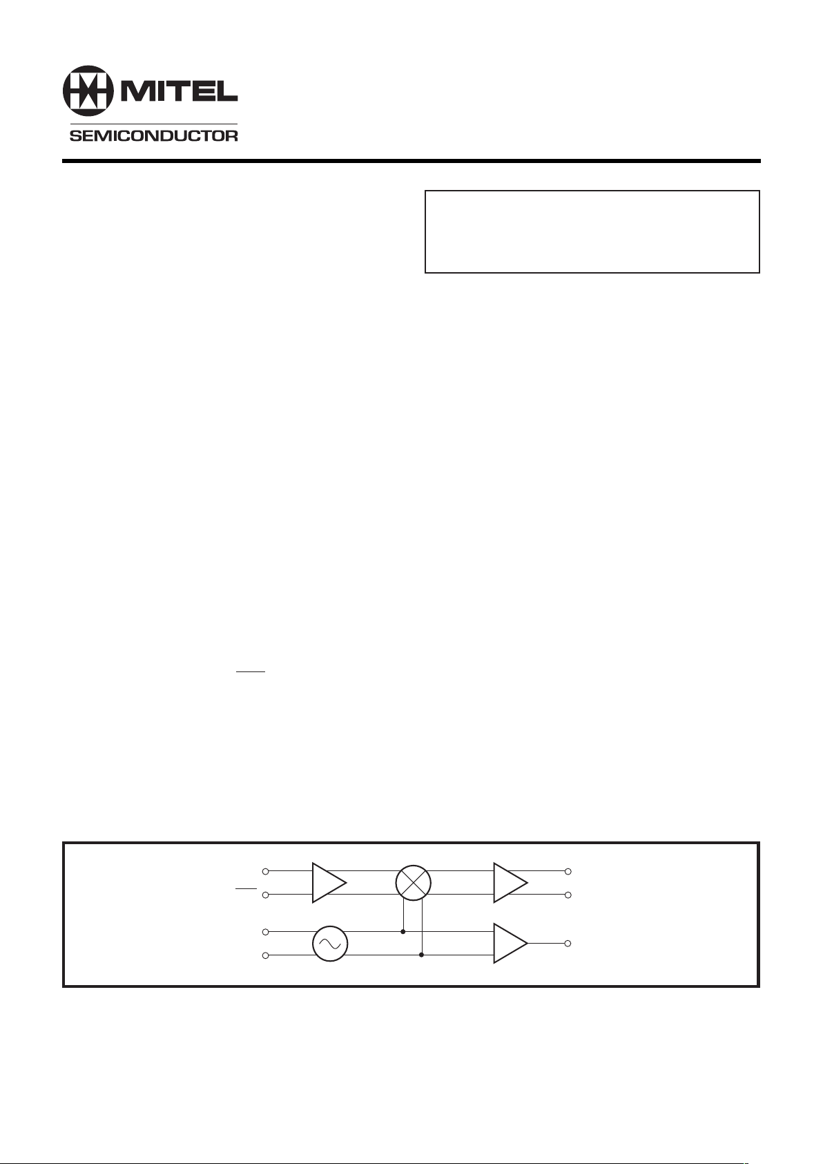
The SL2035 is a bipolar, broadband wide dynamic range
mixer oscillator, optimised for applications as the
downconverter in double conversion tuner systems. It also
has application in any system where a wide dynamic range
broadband frequency converter is required.
The SL2035 is a single chip containing all necessary active
circuitry and simply requires an external tuneable resonant
network for the local oscillator. The block diagram is shown
in Figure 1 and pin connections are shown in Figure 2.
In normal application the signal from the high IF output is
connected to the RFIN and RFIN inputs. The RF input
preamplifier of the device is designed for low noise figure
within the operating region and for high intermodulation
distortion intercept so offering good signal to noise plus
composite distortion spurious performance.
The preamplifier also provides gain to the mixer section
and back isolation from the local oscillator section. The
approximate model of the RF input is shown in Figure 3.
Absolute Maximum Ratings
Supply voltage, V
CC
RF differential input voltage
All I/O port DC offset
Storage temperature
Junction temperature
Package thermal resistance
Chip to ambient, θ
JA
Chip to case, θ
JC
20·3V to 17V
2·5V
20·3 to VCC 10·3V
255°C to 1150°C
1150°C
20°C/W
80°C/W
The output of the preamplifier is fed to the mixer section
which is optimised for low radiation application. In this stage
the RF signal is mixed with the local oscillator frequency,
which is generated by an on-chip oscillator. The oscillator
block uses an external tuneable network and is optimised
for low phase noise. A typical application is shown in
Figure 5. This block also contains a buffer-amplifier to
interface with an external PLL to allow for frequency
synthesis of the local oscillator.
The IF output can be loaded either differentially or singleended. It is recommended that the differential load as in
Figure 5 is applied as this gives best noise performance. If
the output is loaded single-ended the noise figure will be
degraded. The approximate model of the IF output is shown
in Figure 4.
In application care should be taken to achieve symmetric
balance to the IF outputs to maximise intermodulation
performance.
Figure 1 SL2035 block diagram
RFIN
RFIN
LO2
LO1
IF1
IF2
PRSC1
Page 2
2
SL2035
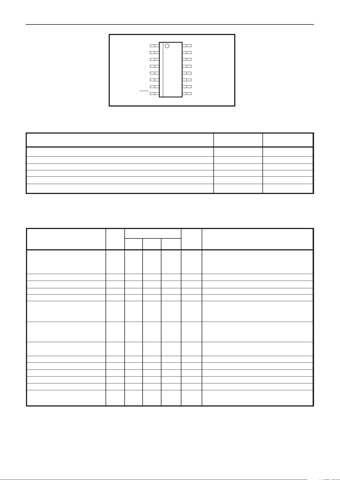
Figure 2 Pin connections - top view
Quick Reference Data
All data applies with circuit component values given in Table 1
Characteristic
Value Units
MP16
SL
2035
1
2
3
4
5
6
7
8
16
15
14
13
12
11
10
9
IF2
NC
GND
GND
GND
GND
RFIN
RFIN
IF1
NC
V
CC
/VCO
LO2
LO1
V
CC
/VCO
PRSC1
VCC/LNA
Electrical Characteristics
Tamb = 240°C to 185°C, VCC = 5V 65%, VEE = 0V. These characteristics are guaranteed by either production test or
design. They apply within the specified ambient temperature and supply voltage ranges unless otherwise stated.
Characteristic Conditions
Max.
Min.
Value
Typ.
Units
IF output pins 1 and 16 will be nominally
connected to VCC through the differential
balun load as in Figure 5
Operating condition only
See Figure 3
See Note 1
T
AMB
= 27°C, with input matching network
as in Figure 5.
With differential load
Differential voltage gain to 50Ω load on
output of impedance transformer as in
Figure 5
Channel bandwidth 8MHz within operating
frequency range
995-1305MHz
See Note 1
Application as Figure 5. See Note 2
Application as Figure 5
Application as Figure 5
Compatible with all standard IF frequencies,
determined by application
Pin
99
1300
221
13
12
14
0·5
220
125
1·4
288
TBA
60
9,11,14
7,8
7,8
7,8
7,8
12,13
1,16
1000
27
9
8
116
0·9
295
30
97
10
11
118
290
mA
MHz
dBµV
dB
dB
dB
dB
dB
dBµV
GHz
dBc/Hz
dBc/Hz
MHz
Supply current
Input frequency range
Composite peak input signal
Input impedance
Input return loss
Input noise figure
Conversion gain
Gain variation within channel
Through gain
IIP3
LO operating range
LO phase noise, 10kHz offset
LO phase noise floor
IF output frequency range
cont…
NOTES
1. Any two tones within RF operating range at 92dBµV with output load as in Figure 5.
2. Use low side LO injection.
RF input operating frequency range
Input noise Figure, SSB
Conversion gain
IIP3 input referred
P1dB input referred
LO phase noise at 10 kHz offset, fRF 1 to 1·3GHz, application as in Figure 5
1000-1300
12
11
118
106
,290
MHz
dB
dB
dBµV
dBc
dBc/Hz
Page 3

3
SL2035
Electrical Characteristics (continued)
95
25
Characteristic
To device input
To device input
Into 50Ω load
See Figure 4
Conditions
Max.
Min.
Value
Units
dBµV
dBµV
dBµV
Ω
Ω
Typ.
72
92
75
LO and harmonic leakage
to RF input
Fundamental
2nd harmonic
LO Prescaler output swing
LO Prescaler output impedance
IF output impedance
Pin
7,8
7,8
10
10
1,16
3·3p
6
6
820
PIN 7
PIN 8
2p
325
PIN 1
PIN 16
Figure 3 Approximate model of RF input Figure 4 Approximate model of IF output
Application Notes
Figure 5 shows the SL2035 in a typical downconverter
application.
The network connected to RF input pin 7 and pin 8 is to
improve the matching between the device input and the
source. The source would normally be from the 1·1MHz
IF output of the upconverter (SL2030) via passive BPF
and gain stage all designed for 50Ω characteristic
impedance.
The network connected to the IF output pin 1 and pin 16 is
a narrow band tuned balun centred typically on 40MHz.
This matches the device output impedance of nominally
400Ω (balanced) to 50Ω (unbalanced).
The network connected to the LO pin 12 and pin 13 is a
varactor diode loaded resonant microstrip line resonator.
Fine adjustment of the tuning range can be achieved by
physically moving C19 (see Figure 5) closer to the LO pins.
This extends the bottom end of the tuning range.
It is important to provide good decoupling on the 5V
supplies and to use a layout which provides some isolation
between the RF, IF and LO ports.
Page 4

4
SL2035
Figure 5 SL2035 upconverter application
SL
2035
1
2
3
4
5
6
7
8
16
15
14
13
12
11
10
9
IF2
GND
GND
GND
GND
RFIN
RFIN
IF1
V
CC
/VCO
LO2
LO1
V
CC
/VCO
PRSC1
V
CC
/LNA
L8
C5
C4
IF OUT
S1 RESONATOR
C19
C10 C13
V
CC2
C17 C9
V
CC1
C18 C8
C3
R12
SKT2
C21
SKT1
RFIN
C2
C1
L5
C23
D1
V
CC3
C15
C14
C24
R9
R10
C22
EXTERNAL
VARACTOR DRIVE
(REMOVE R9)
SKT4
L7
C52
V
CC1
L6
C53
V
CC2
L3
C54
V
CC3
5V DEVICE SUPPLY
2
1
1
2
3
GND
30V
5V
30V SYNTHESISER
GND
5V SYNTHESISER
J2
POWER
J1
POWER
C11
T1
BCW31
130V
15V
SP
5659
1
2
3
4
5
6
7
8
16
15
14
13
12
11
10
9
CP
XTAL
REF/COMP
ADDRESS
SDA
SCL
P3
P2
DRIVE
V
EE
RF I/P
RF I/P
V
CC
ADC
P0
P1
C42
R7
C31
R8
L9
C4
X1
C30
C38C47
15V
C43 C46
R11
SCL5
5V
SDA5
J3
3
4
5
6
I2C BUS
NOTE: Refer to Table 1 for component values
C41
L10
C6
SKT3
L11
C37 NC
C34
Page 5

5
SL2035
0·5
1·0
1·5
1·5
3 3 3
0·5
0·5
Table 1 Component values for Figure 5
Figure 6 Microstrip resonator (dimensions are in mm)
C41
C42
C43
C46
C47
D1
L3
L5
L6
L7
L8
L9
L10
L11
R7
R8
R9
R10
R11
R12
S1
T1
X1
C1
C2
C3
C4
C5
C8
C9
C10
C11
C13
C14
C15
C17
C18
C19
C21
C22
C23
C24
C30
C31
C34
C36
C37
C38
Component
1nF
1nF
1 nF
10nF
56pF
100pF
100pF
100pF
10µF
100nF
100nF
100pF
100nF
100nF
2pF
1nF
33nF
47pF
1nF
18pF
330nF
100nF
56pF
NC
100nF
Value/type Component
4·7µF
3·3nF
100nF
100pF
100pF
IT397
220nH
1·8nH
220nH
220nH
1µH
220nH
680nH
680nH
15kΩ
22kΩ
15kΩ
1kΩ
4·7kΩ
50Ω
Resonator (Figure 6)
BCW31
4MHz crystal
Value/type
Page 6

M Mitel (design) and ST-BUS are registered trademarks of MITEL Corporation
Mitel Semiconductor is an ISO 9001 Registered Company
Copyright 1999 MITEL Corporation
All Rights Reserved
Printed in CANADA
TECHNICAL DOCUMENTATION - NOT FOR RESALE
World Headquarters - Canada
Tel: +1 (613) 592 2122
Fax: +1 (613) 592 6909
North America Asia/Pacific Europe, Middle East,
Tel: +1 (770) 486 0194 Tel: +65 333 6193 and Africa (EMEA)
Fax: +1 (770) 631 8213 Fax: +65 333 6192 Tel: +44 (0) 1793 518528
Fax: +44 (0) 1793 518581
http://www.mitelsemi.com
Information relating to products and services furnished herein by Mitel Corporation or its subsidiaries (collectively “Mitel”) is believed to be reliable. However, Mitel assumes no
liability for errors that may appear in this publication, or for liability otherwise arising from the application or use of any such information, product or service or for any infringement of
patents or other intellectual property rights owned by third parties which may result from such application or use. Neither the supply of such information or purchase of product or
service conveys any license, either express or implied, under patents or other intellectual property rights owned by Mitel or licensed from third parties by Mitel, whatsoever.
Purchasers of products are also hereby notified that the use of product in certain ways or in combination with Mitel, or non-Mitel furnished goods or services may infringe patents or
other intellectual property rights owned by Mitel.
This publication is issued to provide information only and (unless agreed by Mitel in writing) may not be used, applied or reproduced for any pur pose nor form par t of any order or
contract nor to be regarded as a representation relating to the products or services concerned. The products, their specifications, services and other information appearing in this
publication are subject to change by Mitel without notice. No warranty or guarantee express or implied is made regarding the capability, performance or suitability of any product or
service. Information concerning possible methods of use is provided as a guide only and does not constitute any guarantee that such methods of use will be satisfactory in a specific
piece of equipment. It is the user’s responsibility to fully determine the performance and suitability of any equipment using such information and to ensure that any publication or
data used is up to date and has not been superseded. Manufacturing does not necessarily include testing of all functions or parameters. These products are not suitable for use in
any medical products whose failure to perform may result in significant injury or death to the user. All products and materials are sold and services provided subject to Mitel’s
conditions of sale which are available on request.
 Loading...