

Page 1

SL3522
500MHz 75dB Logarithmic/Limiting Amplifier
Advance Information
Supersedes edition in Professional Products IC Handbook May 1991 DS3534 - 2.0 April 1994
The SL3522 is a monolithic seven stage successive
detection logarithmic amplifier integrated circuit for use in the
100MHz to 500MHz frequency range. It features an on–chip
video amplifier with provision for external adjustment of log
Slope and offset. It also features a balanced RF output. The
SL3522 operates from supplies of ±5V.
FEATURES
■ 75dB Dynamic Range
■ Surface Mount SO Package
■ Adjustable Log Slope and Offset
■ 0dBm RF Limiting Output
■ 60dBm Limiting Range
■ 2V Video Output Range
■ Low Power (Typ. 1W)
■ Temperature Range (T
): -55°C to +125°C
CASE
RF O/P GND
RF O/P–
RF O/P+
RF O/P V
VIDEO O/P V
VIDEO O/P
VIDEO O/P V
N/C
N/C
V
GND
V
GND
V
EE
EE
EE
EE
EE
CC
128
2
3
4
5
6
7
8
9
10
11
12
13
14
Fig.1 Pin connections - top view
27
26
25
24
23
22
21
20
19
18
17
16
15
RF I/P+
RF I/P–
V
EE
GND
V
EE
GND
V
EE
GND
VIDEO V
EE
GAIN ADJUST
TRIM REF
OFFSET ADJ
VIDEO GND
VIDEO V
CC
MC28
APPLICATIONS
■ Ultra Wideband Log Receivers
■ Channelised and Monpulse Radar
■ Instrumentation
ABSOLUTE MAXIMUM RATINGS
Supply Voltage ±6.0V
Storage temperature -65°C to +175°C
Junction temperature +175°C
Thermal resistance
Die-to-case 15.5°C/W
Die-to-ambient 76.5°C/W
Applied DC voltage to RF input ±400mV
Applied RF power to RF input +15dBm
RF
27
I/P –
RF
I/P +
28
ORDERING INFORMATION
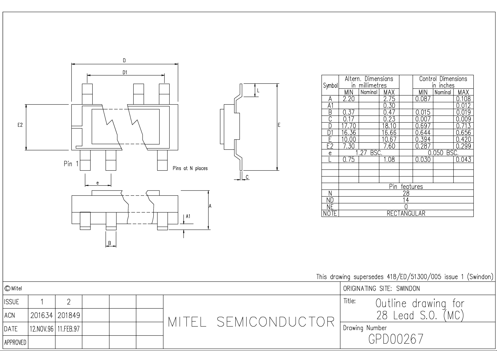
SL3522 A MC (Miniature Ceramic package)
SL3522 C MC (Miniature Ceramic package)
SL3522 NA 1C (Probe-tested bare die)
(Also available: SL3522 AA MC screened to Mitel HI-REL
level A. Contact Mitel Semiconductor sales outlet for a
separate datasheet.)
ESD PROTECTION
To achieve the high frequency performance there are no
ESD protection structures on the RF input pins (27, 28). These
pins are highly static sensitive, typically measured as 250V
using MIL-STD-883 method 3015. Therefore, ESD handling
precautions are essential to avoid degradation of
performance or permanent damage to this device.
RF
RF
O/P–
91014
VIDEO GAIN
AND OFFSET
O/P+
ADJUST
O/P
V
CC
16
13
12
15
O/P
GND
VIDEO
OUT
O/P
V
EE
VIDEO
V
CC
3, 5, 7, 20, 22, 24, 26 V
4, 6, 8, 21, 23, 25 GND
EE
Fig.2 Functional block diagram
19 18 17
GAIN
ADJ
RTR
R
G
OFFSET
O
ADJ
Page 2

SL3522
ELECTRICAL CHARACTERISTICS
The electrical characteristics are guaranteed over the following range of operating conditions, using test circuit in Fig. 3 (unless
otherwise stated):
Temperature range: Military: SL3522 A MC, SL3522 NA 1C 55°C to +125°C (T
Commercial: SL3522 C MC 0°C to +70°C (T
CASE
Supply voltage: VCC: +4.50V to +5.50V (all grades)
VEE: -4.5V to -5.50V (all grades)
Frequency =100MHz to 500MHz
Rg, Ro, Rt =1.5KΩ
Video output load =200Ω//20pF
Test conditions (unless otherwise stated):
Temperature: SL3522 A MC: +25°C, +125°C & -55°C (T
CASE
)
SL3522 C MC: +25°C
SL3522 NA 1C +25°C
Supply voltage: VCC = +5.0V, VEE = -5.0V
Parameter
Pin
Value
Units
Conditions
Min. Typ. Max.
Positive supply current
14, 15
28
35
mA
V
CC
= +5.0V
(quiescent)
Negative supply current
(quiescent)
Dynamic range
Linearity
Video output range
Video slope
Video slope variation
Video slope adjust range
Video offset
Video offset variation
Video offset adjust range
Video trim reference
voltage
Video output impedance
Video rise time
ALL V
Pins
13
13
13
13
13
13
13
17, 18,
19
13
13
EE
75
70
-1
-1
-1.25
1.30
18
-5
±20
-0.1
±0.5
-0.59
150
180
1.75
21
±30
+0.25
-05
-0.54
10
16
175
210
+1
+1
+1.25
2.00
24
+5
+0.5
-0.49
mA
mA
dB
dB
dB
dB
dB
V
mV/dB
%
%
V
mV/°C
V
V
Ω
ns
= -5.0V See note 1
V
EE
V
= -5.0V See note 2
EE
100 to 400MHz See note 1, 3
See note 1, 4
T
= -55°C
CASE
T
= +25°C
CASE
T
= +125°C
CASE
See note 5
RG = 1kΩ to 2.2kΩ
= +25°C
T
CASE
RO = 1kΩ to 2.2kΩ
See note 8
10% - 90% (60dB step)
See note 7
Input VSWR
RF bandwidth
27, 28
9, 10
1.5:1
450
MHz
Zs = 50Ω See note 7
TCASE = +25°C RFIN = -70dBm
See notes 2, 7
RF limiting range
RF limited output level
9, 10
9, 10
-3.0
60
-1.0
+1.0
dB
dBm
See notes 2, 6, 7
R1 = 50Ω single ended
See note 2
RF output impedance
9, 10
50
Ω
Single ended See notes 2, 8
CASE
)
)
2
Page 3

ELECTRICAL CHARACTERISTICS (cont.)
Parameter
Pin
Value
Min. Typ. Max.
Units
SL3522
Conditions
Phase variation with RF
Input level
Phase tracking between
units
15
Degrees
3
Degrees
Freq = 300MHz RF
See notes 2, 7
T
= +25°C FREQ = 300MHz
CASE
See notes 2, 7
= -60 to +10dBm
IN
Notes
1 RF output buffer OFF (pin 8 disconnected from 0V)
2 RF output buffer ON (pin 8 connected to 0V)
3 Minimum dynamic range under any single set of operating conditions
4 Log linearity guaranteed for pin = -64dBm to +6dBm for ALL supply, temperature and frequency conditions
5 Full range of supply, temperature and frequency conditions
6 Input limiting range typically -50dBm to +10dBm
7 Not tested, but guaranteed by characterisation
8 Not tested, but guaranteed by design
The SL3522 CANNOT be GUARANTEED to operate below 100MHz and meet the electrical characteristics shown above.
However, characterisation has shown that the device can still function adequately down to frequencies of 50MHz, with the following
reservations:-
1)The video bandwidth is fixed to approx 40MHz a certain amount of carrier breakthrough on the video O/P (pin 13) will occur,
with input signal frequencies below 100MHz.
2)There are 2 RF coupling capacitors (20pF) on-chip, which couple the output signal from stage 3 to the input of stage 4 (ref
Fig. 24). These can introduce undesirable limiting phase performance for input signal frequencies below 100MHz.
RF INPUT
123
ANZAC
TP101
654
L1
10n
L2
GAIN
ADJUST
R
2k2
G
10n
R
1k5
T
OFFSET
ADJUST
2k2
R
0
+5V V
CC
262728
321
10n
+5V V
EE
NOTES
1. Inductors L1 to L5 = 3 TURNS
2. D.U.T. mounted in a test socket
3. Transmission line BALUNS used
30SWG on Ferrite bead.
– ENPLAS OTS–28–1.27–04
– not recommended in Application (see Para 3C)
SL3552
SW1
Fig.3 Test circuit
10n
1n 1n
100
654
ANZAC
TP101
123
L4
RF OUTPUT
L5
10n
10n
1516171819202122232425
L3
1413121110987654
10n
VIDEO
470
18p200
OUTPUT
3
Page 4
SL3522
PRODUCT DESCRIPTION
The SL3522 is a complete monolithic successive detection
Log/limiting amplifier which can operate over an input
frequency range of 100MHz to 500MHz. Producing a log/lin
characteristic for input signals between -64dBm and +6dBm,
the log amplifier can provide an accuracy of better than
±1.00dB at case temperatures of -55°C and +25°C and an
accuracy of better than ±1.25dB at +125°C. The dynamic
range is better than 75dB over a frequency range of 100MHz
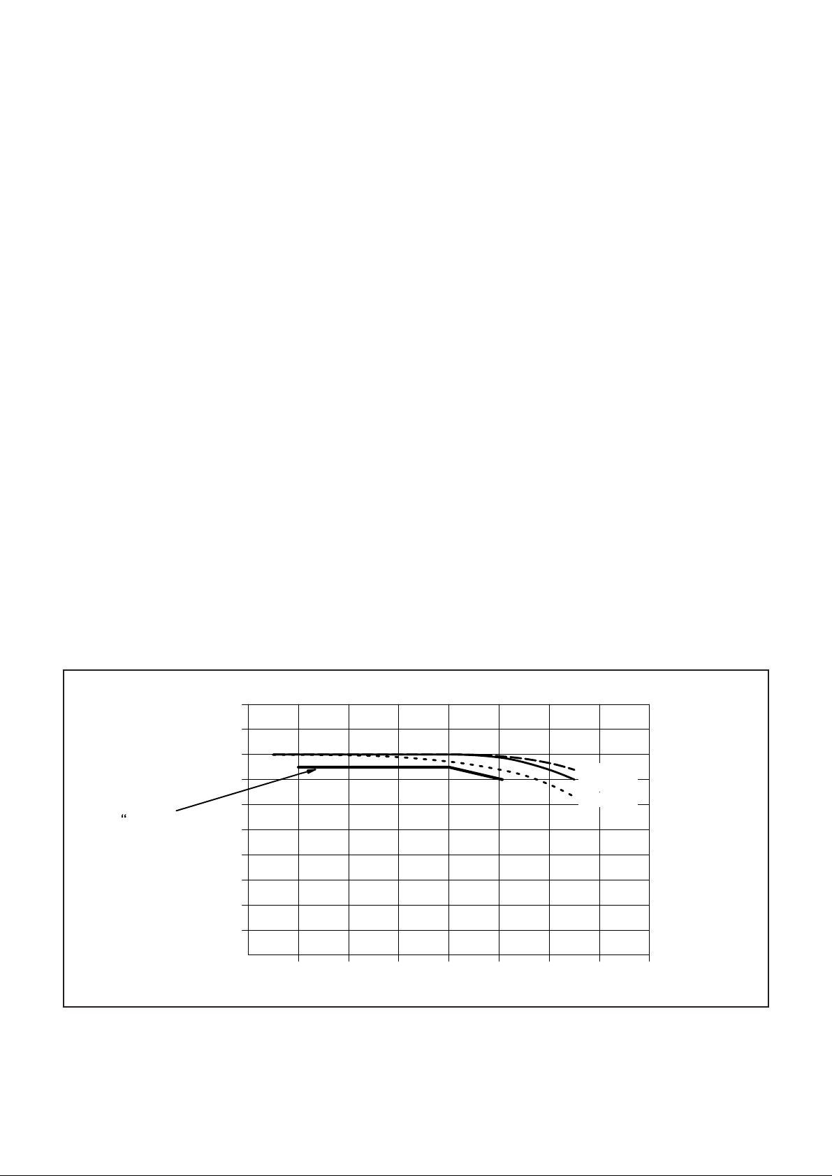
to 400MHz. The graph in fig 4 shows how the dynamic range
is guaranteed over frequency.
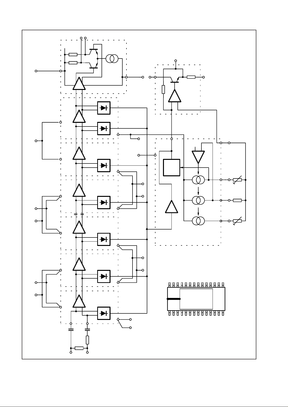
The SL3522 consists of 6 Gain stages, 7 Detector stages,
a limiting RF Output buffer and a Video Output amplifier. The
power supply connections to each section are isolated from
each other to aid stability.
The SL3522 consumes 1.1W of power when ALL parts of
the circuit are powered up from a ±5.0V power supply. As the
circuit uses a differential architecture, the power consumption
of the RF gain/detector stages and RF Output Buffer will be
independent of RF input signal level. However, the Video
Output (pin 13) is driven by a single ended emitter follower and
so the power consumption of the Video amplifier will vary with
RF input signal level between pins 27 and 28.(upto 10mA over
2V video output range with max video load of 200Ω //20pF) The
SL3522 has a high RF gain (>50dB) across a wide bandwidth
(>450MHz) when the limiting RF Output Buffer is enabled. The
limiting RF Output Buffer provides a balanced Limited Output
level of nominally –1.0dBm on each RF Output connection (pin
9 and 10), for RF input signal levels on pins 27 and 28 in excess
of –50dBm.
The limiting RF Output Buffer can be isolated from the
other sections of the SL3522, by disconnecting the RF Output
Buffer GND (pin 8) from 0V, and leave the pin floating. This
feature aids stability in applications NOT requiring a Limited RF
Output signal, and lowers the power consumption of the
SL3522 to 0.95Watts, when the other sections are powered up
from a ±5.0V power supply.
Each of the Gain and Detector stages has approximately
12dB of gain, and a significant amount of on-chip RF
decoupling (200pF per stage), also to aid stability. The Video
amplifier provides a positive going output signal proportional to
the log of the amplitude of an RF input applied between pins 27
and 28. The gain and the offset of the Video amplifier can be
adjusted by 3 resistors; R
, RT , and RO which are connected
G
to Gain adjust (pin 19),Trim reference (pin 18) and Offset
adjust (pin 17). With R
set to 1.5kΩ , R
T
can be set to any value
G
between 1kΩ and 2k2Ω and achieve a range in Video Slope of
±20%, centred on 21mV/dB. Similarly, R
can be set to any
O
value between 1kΩ and 2.2KΩ and achieve an offset range of
±0.5V, which should allow the Video Offset to be trimmed to 0V
if required.
The RF input pins (27 and 28) have a 50Ω terminating
resistor connected between them on–chip. These are
capacitively coupled to the I/P gain stage with 20pF on-chip
capacitors. (Refer to APPLICATION NOTES section for
information on how to connect an RF input signal to the device).
100
90
Minimum
guaranteed
dynamic
range (dB)”
80
70
60
50
40
30
20
10
0
100 200 300 400 500 600 700 800
–55°C
+25°C
+125°C
Fig.4 Plot showing guaranteed dynamic range v. frequency
(typical achievable dynamic range lines indicated across temperature)
4
Page 5

APPLICATION NOTES
SL3522
1) VIDEO–AMPLIFIER
The SL3522 uses a single ended Video amplifier to
produce a trimmable Video transfer characteristic. Both the
gain (Slope) and Offset of the amplifier can be externally
adjusted.
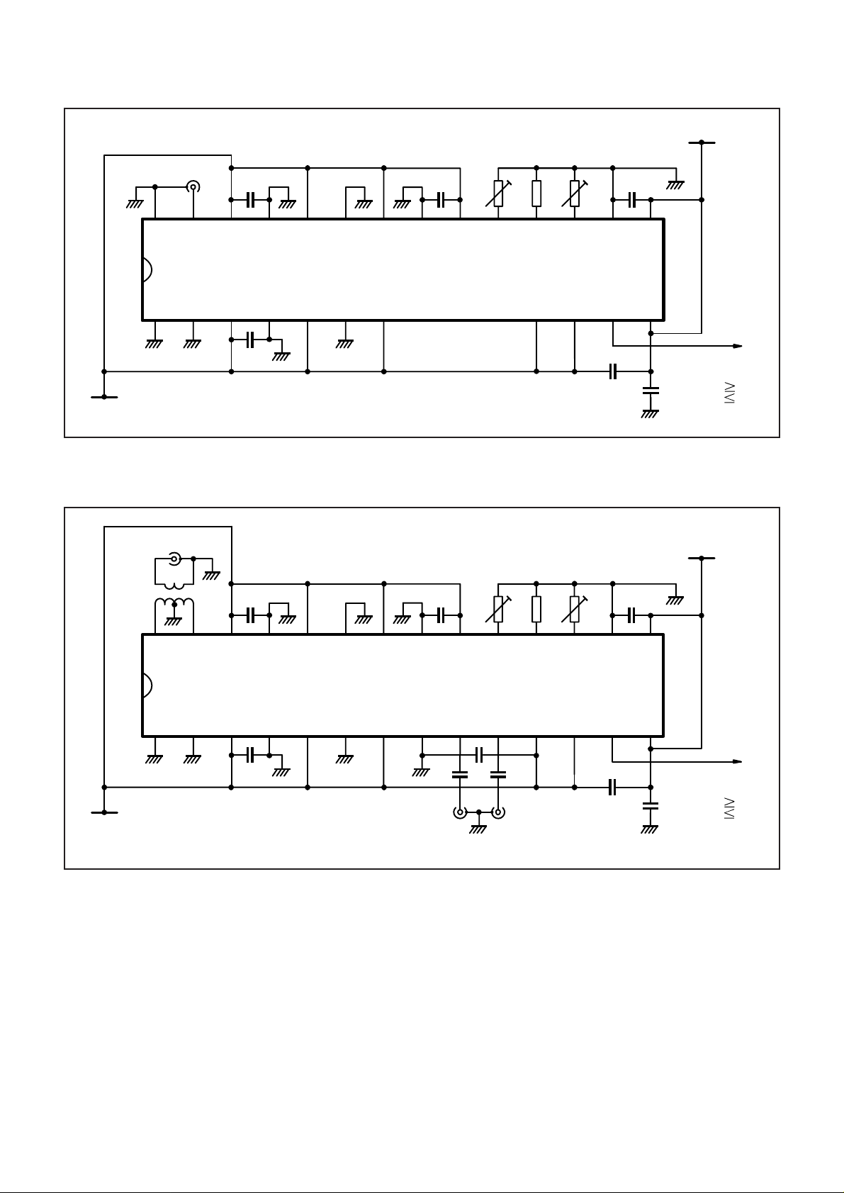
a) Gain and Offset trimming (ref Applications
circuits in figs 5 and 6)
The Gain and Offset control is achieved by adjusting R
and R
respectively. The control is dependent upon their
O
difference from the Trim reference resistor, RT. Adjustment of
Gain has an effect on Offset, but adjustment of Offset does
NOT affect the Gain. Therefore the Gain should be optimised
first. The Offset should only be adjusted once the Gain has
been set.
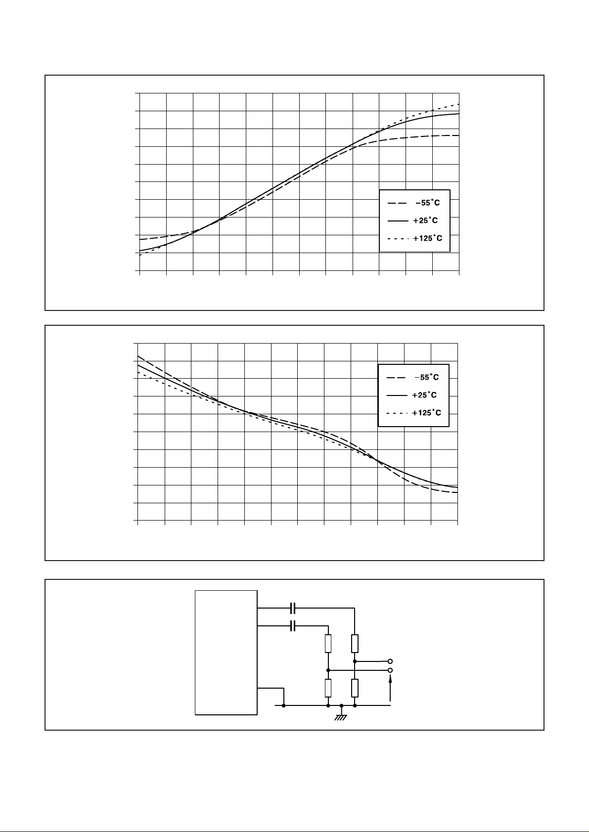
Fig 7 shows the variation of Video Offset with value of RO,
for a fixed value of R
and RG = 1k5Ω.
T
Fig 8 shows the variation of Video Slope with value of RG,
for a fixed value of R
and RO = 1k5Ω.
T
The Video amplifier incorporates temperature
compensation for Video gain (Slope). To ensure temperature
stability for Video gain (Slope) over the operating temperature
range, it is recommended that the resistors with identical
temperature coefficients of resistance are used for R
and R
T
The Video amplifier does NOT incorporate temperature
compensation for Video Offset. Although it is recommended
that a resistor with identical temperature coefficient of
resistance to R
be used for R
T
, it may be necessary to use an
O
additional external temperature compensating network.
b) Video performance
The Video–amplifier has a critically damped rise time of
16ns (10% - 90%).In order to achieve this transient
performance, it is important to ensure that:-
i) the resistor connected to Trim reference (pin 18), has a
nominal resistance of 1.5kΩ, with a parasitic capacitance
LESS than 5pF.
ii) the load applied to the Video Output (pin 13) does NOT
exceed 200Ω resistance in parallel with 20pF.
Also, the following decoupling should be incorporated:-
i) The Video Output V
(pin 14) should be decoupled with
CC
a 10nF capacitor to the RETURN line from the video load,
connected to Video GND (pin 16), avoiding any common
impedance path.
ii) The Video Output Vee (pin 12) should be decoupled
with a 10nF capacitor DIRECTLY to Video-Output VCC (pin
14).
2) SL3522 AS A LOG AMPLIFIER
with RF output buffer disabled (pin 8 floating)
If the SL3522 is to be used as a Logarithmic successive
detection amplifier only, with no requirement for a limited RF
Output, the RF input (pins 27 and 28) can be driven EITHER
differentially or single ended from a 50Ω source. If being used
with a single ended input, the SIGNAL should be applied to pin
27 and the RETURN should be connected to pin 28, as shown
in the Application circuit diagram in Fig 5.
The SL3522 is VERY stable when used in this way.
Although not a crucial requirement, it is recommended that the
device should be mounted using a ground plane.
3) SL3522 AS A LOG/LIMITING AMPLIFIER
- with RF Output-Buffer ENABLED (pin 8 connected
to GND)
If the SL3522 is to be used as a Limiting or Log/limiting
amplifier with a requirement for a Limited RF Output signal,care
is required in the layout of components and connections around
the device to ensure stability. The following precautions should
be observed (refer to Application circuit diagram in Fig. 6):-
G
.
G
a) The device should be mounted on a ground plane,
ensuring that the impedance between the ground plane and
ALL the GND pins is kept as low as possible. If a multilayer PCB
is used where the ground plane is connected to the GND pins
using through-plated holes (vias), it is essential to ensure that
the vias have a very low impedance. ALL supply decoupling
capacitors should be RF chip capacitors whose leads should be
kept as short as possible.
b) The RF V
connections (pins 3,5,7,11,20,22,24,26)
EE
should be connected to a low impedance copper plane. A two
layer PCB should help to achieve this.
c) The RF input (pins 27 and 28) should be driven with a
balanced source impedance. One way of achieving this is to
use an isolating BALUN transformer (50Ω UNBALANCED →
50Ω BALANCED) connected between the signal source and
the RF input pins. (e.g. Mini circuits TT1–6, TO –75). The device
stability is VERY sensitive to an imbalance of the differential
source impedance at pins 27 and 28. Use of a transmission line
BALUN though, is NOT recommended.
d) The RF Output connections (pins 9 and 10) should each
be loaded with matched impedances ideally 50Ω transmission
lines. The RF Output lines leading away from the device should
be balanced. Driving highly reactive SWR loads is NOT
recommended as these can encourage device instability, as
can an imbalance of the differential load impedance at pins 9
and 10.
e) The RF Output connections (pins 9 and 10) are DC
coupled, and ideally the output pins should be capacitively
coupled to their loads using 1nF capacitors. However the RF
Outputs can drive a DC load to GND and a DC offset of approx.
400mV will exist on each RF Output pin. IT WILL NOT BE
POSSIBLE TO DISABLE THE RF OUTPUT BUFFER UNDER
THESE CONDITIONS.
f) The RF output (pins 9 and 10) has a tendancy to limit on
self noise, particularly at low ambient temperatures (-55°C),
when the RF output buffer is enabled.
NOTE that this will effect the liminting range as the gain of the
RF output buffer will reduce as the amount of noise limiting
increases.
If required the limited RF Output can be attenuated using
an attenuation network as shown in fig. 9. Under these
conditions the effective RF Output currents will be reduced,
allowing the device to operate with a greater margin of
stability.It may be possible to run the device without a BALUN
transformer on the RF input if the total output impedance on the
RF Output >> 50Ω , and the attenuation components are
mounted as close as possible to the RF Output connections
(pins 9 and 10). The RF input connection could then be
configured as in Fig 5.
5
Page 6
SL3522
–5V V
EE
RF INPUT
RF INPUT
10n
10n
GAIN
ADJUST
R
2k2
G
R
1k5
T
OFFSET
ADJUST
R
2k2
0
262728
SL3522
321
10n
10n
Fig.5 Application circuit successive detection logarithmic function only
10n
10n
GAIN
ADJUST
R
2k2
G
R
1k5
T
OFFSET
ADJUST
R
2k2
0
10n
10n
+5V V
CC
1516171819202122232425
1413121110987654
10n
+5V V
VIDEO
OUTPUT
VIDEO
LOADING
R
200
C 20p
CC
–5V V
EE
262728
1516171819202122232425
SL3522
10n
1413121110987654
10n
VIDEO
OUTPUT
VIDEO
LOADING
R
200
C 20p
321
10n
10n
1n
1n
RF OUTPUT
Fig.6 Application circuit - Log / Limiting function
6
Page 7
1.50
1.25
1.00
.75
.50
.25
0.00
Video offset (V)
–.25
–.50
–.75
–1.00
Fig.7 Video offset v. offset-adjust resistor (pin17 to gnd) across temperature
SL3522
22001000 1100 1200 1300 1400 1500 1600 1700 1800 1900 2000 2100
Offset–adjust resistor (ohms)
30
28
26
24
22
20
18
16
Video slope (mV/dB)
14
12
10
1000 1100 1200 1300 1400 1500 1600 1700 1800 1900 2000 2100
Gain–adjust resistor (ohms)
Fig.8 Video slope v. gain-adjust resistor (pin19 to gnd) across temperature
RF O/P–
RF O/P+
9
10
1n
1n
2200
SL3522
R1 R1
RF O/P GND
Fig.9 Network for attenuating limited RF output
8
50 50
7
Page 8
SL3522
A PRACTICAL APPLICATION FOR THE SL3522
AS A LOG/LIMITING AMPLIFIER
The SL3522, with the RF Output-Buffer ENABLED, has a
large limited RF Output level (0dBm on each of two RF Output
pins (9 and10)) and a wide RF bandwidth (450MHz) in a small
28 pin Miniature Ceramic S.O package. As a result, there is a
tendency for the device to become unstable unless care is
used in the application.
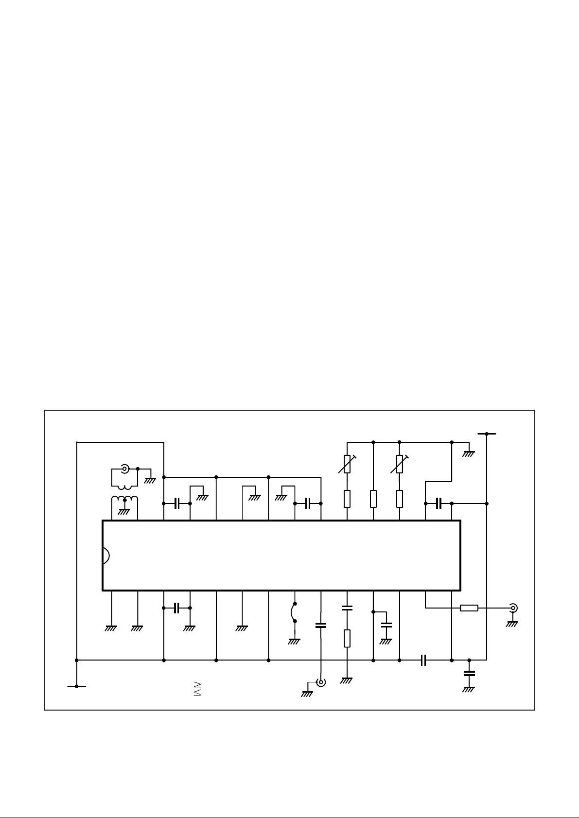
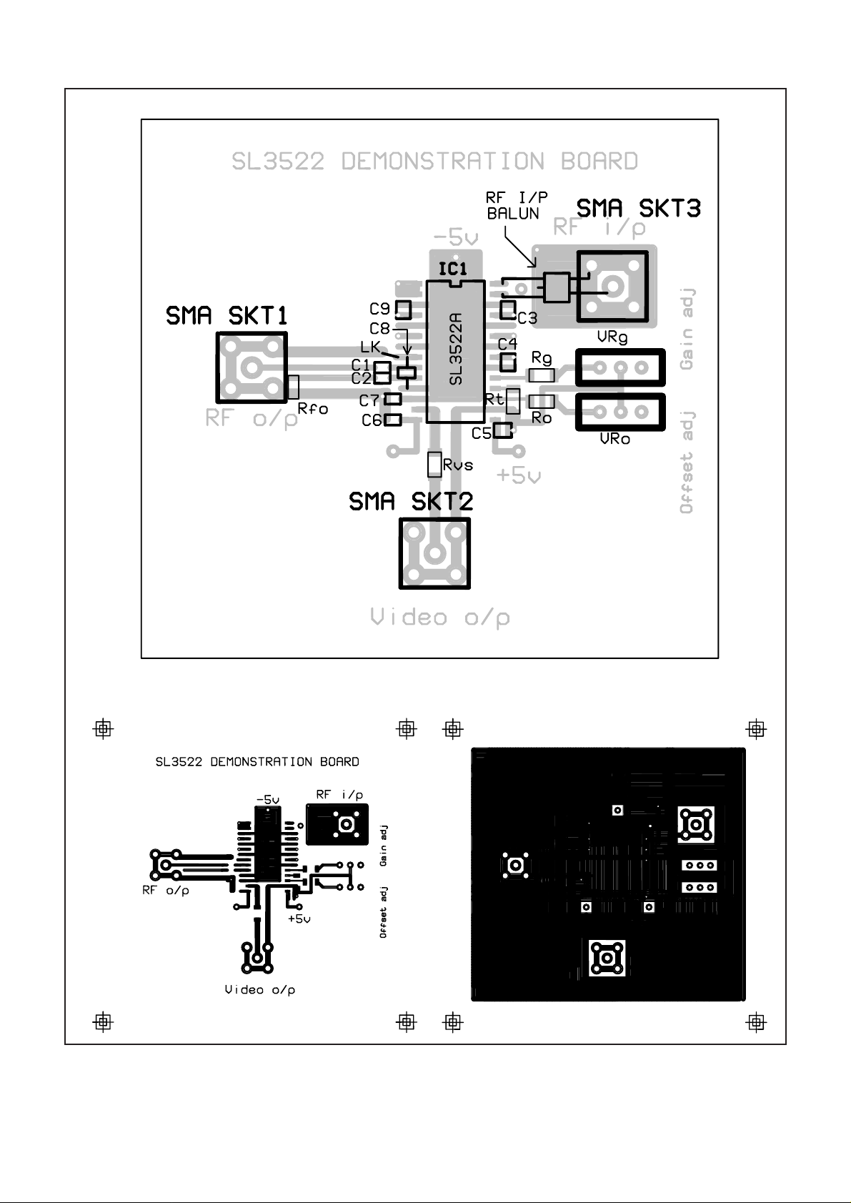
The PCB layout for a ”SL3522 DEMONSTRATION
BOARD” in Fig. 11 has proved reliably stable. The PCB is a
double layer Fibre epoxy board which uses SMDs where
possible. A circuit diagram for the Demonstration PCB appears
in Fig. 10.
The following points should be noted when this
application is realised practically:-
1) A wire needs to connect the two pads connected to pins
14 and 15 of the SL3522, to allow +5V to appear at both pins.
2) ALL the GND connections to the SL3522 are made
through the PCB to a Ground plane on the bottom side. It is
important to ensure that the impedance of each of these
connections is kept to an absolute minimum to prevent
instability. If these connections are achieved using through
plated holes, it is recommended that they are filled with solder
to lower their impedance.
3) The PCB is configured to accept SMA, SMB or SMC
connectors for the RF input, RF Output and Video Output
connections. These can be changed if necessary to an
alternative type, but it is vital to ensure that the ground plane
is solidly connected to the Guard Ring which surrounds the RF
Output tracks.
4) The PCB is configured to accept a small surface
mounting DC isolating BALUN transformer (e.g VANGUARD
VE43666, available from Vanguard Electronics Company Inc,
1480 West 178th St. GARDENA, C.A. 90248, U.S.A. Tel:U.S.A. (213) 323 – 4100) to couple a signal into the RF input
connections (pins 27 and 28). It is NOT recommended to
attempt operating the SL3522 with the RF Output Buffer
enabled, WITHOUT using an input BALUN, although it may be
possible, provided the input source impedance to both pins 27
and 28 remains balanced. The centre tap of the secondary
winding of the transformer should be soldered to the small
ground plane on the upper side of the PCB.
5) The RF Output connection to the PCB is from pin 9 of
the SL3522 only, with pin 10 being terminated on the PCB
using a 51Ω resistor. It is important to ensure that both pin 9
and10 are terminated with equal impedances.
6) The RF Output Buffer can be enabled by soldering a
link (LK) between pin 8 of the SL3522 and the adjacent guard
track around the RF Output lines. Similarly, the buffer can be
disabled by removing the same link. When the buffer is
disabled, the following components can be omitted:-
1nF capacitors (C1, C2)
10nF capacitor (C8)
51Ω resistor (R
FO
)
7) The Slope (gain) and Offset of the Video Output can be
adjusted using two 1kΩ trimmers, provision for which is
included in the PCB layout.
The plots in Fig. 12 to fig. 23 are typical of the performance
of SL3522 devices used with the PCB layout detailed in Fig.11.
–5V V
RF INPUT
EE
10n
262728
321
C9
10n
VIDEO LOADING
R 200
C 20p
SL3522
LK
RF OUTPUT
GAIN
ADJUST
VRG 1k
C4C3
10n 10n
C1
1n
R
R
G
1k5
1k
C8
C2
10n
1n
R
FO
51 C7
OFFSET
ADJUST
VR0 1k
C5
R
T
O
1k
10n
+5V V
CC
1516171819202122232425
1413121110987654
R
VS
150
C6
10n
VIDEO
OUTPUT
Fig.10 SL3522 demonstration board circuit diagram
8
Page 9
SL3522
Fig.11 Demonstartion Circuit PCB showing components positions (2x full size) with top and bottom copper masks (full size)
9
Page 10
SL3522
VIDEO O/P (V)
2
1.75
1.5
1.25
1
0.75
0.5
0.25
0
–90 –80 –70 –60 –50 –40 –30 –20 –10 0
RF input power (dBm)
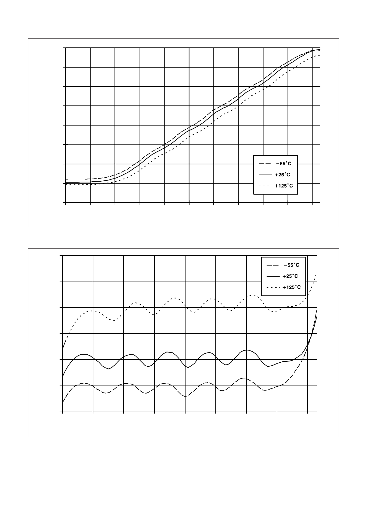
Fig.12 Video O/P vs CW input level at 325MHz across temperature (VCC = +5.0V, VEE = -5.0V)
8
6
4
2
LOG – ERROR (dB)
0
10
–2
–4
–70 –60 –50 –40 –30 –20 –10 0
RF input power (dBm)
10
Fig.13 Video O/P log-error, (referenced to single straight line measured at 325MHz, +25°C, 5.0V PSUs) across temperature
10
Page 11
7
6
5
4
3
2
1
LOG – ERROR (dB)
0
–1
SL3522
4.5V
5.0V
–2
–3
–70 –60 –50 –40 –30 –20 0 10
RF input power (dBm)
–10
5.5V
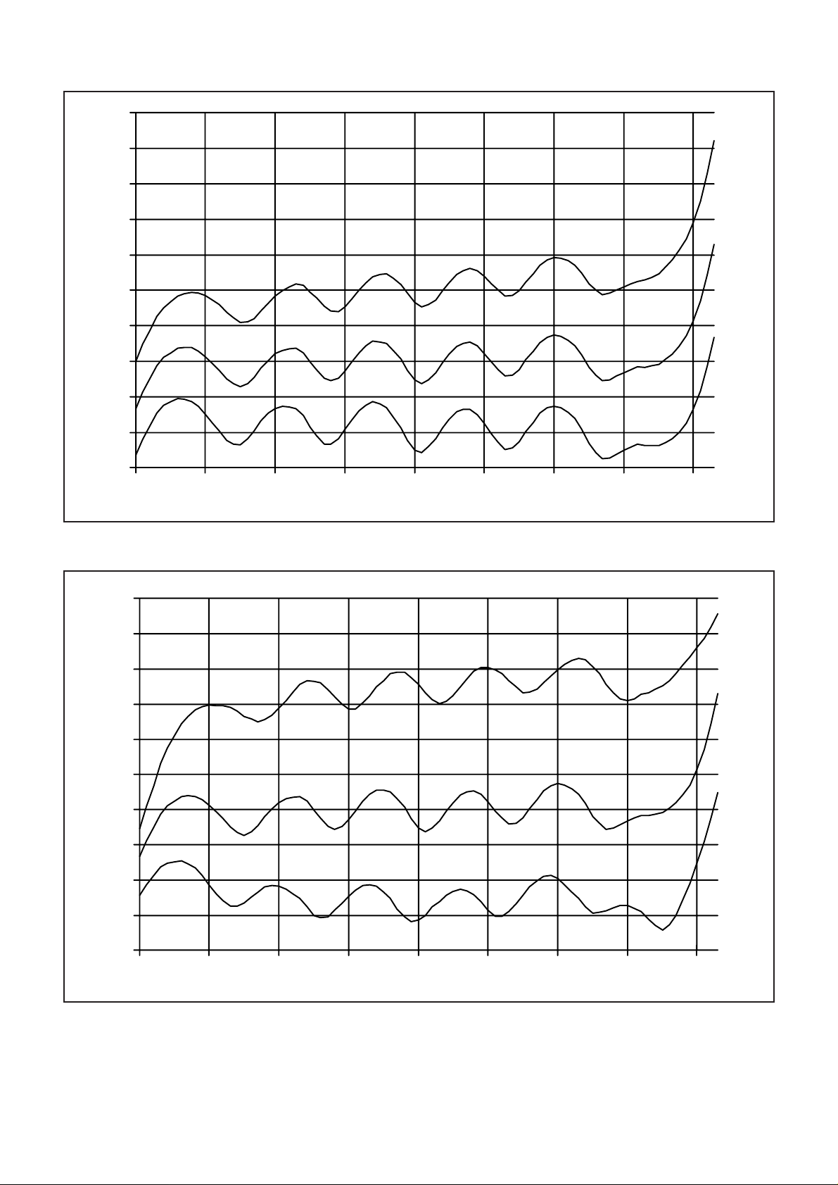
Fig.14 Video log error, (referenced to single straight line measured at 325MHz, 25°C, 5.0V PSUs), across supply voltage
6
5
4
3
2
1
LOG – ERROR (dB)
0
500MHz
325MHz
–1
–2
–3
–4
–70 –60 –50 –40 –30 –20
RF input power (dBm)
Fig.15 Video log error, (referenced to single straight line measured at 325MHz, 25°C,
–10
100MHz
010
11
Page 12
SL3522
70
60
50
40
30
GAIN (dB)
20
10
0
10 110 210 310 410 510 610 710 810 910 1010
Frequency (MHz)
0
–5
–10
–15
–20
–25
RF output power (dBm)
–30
–35
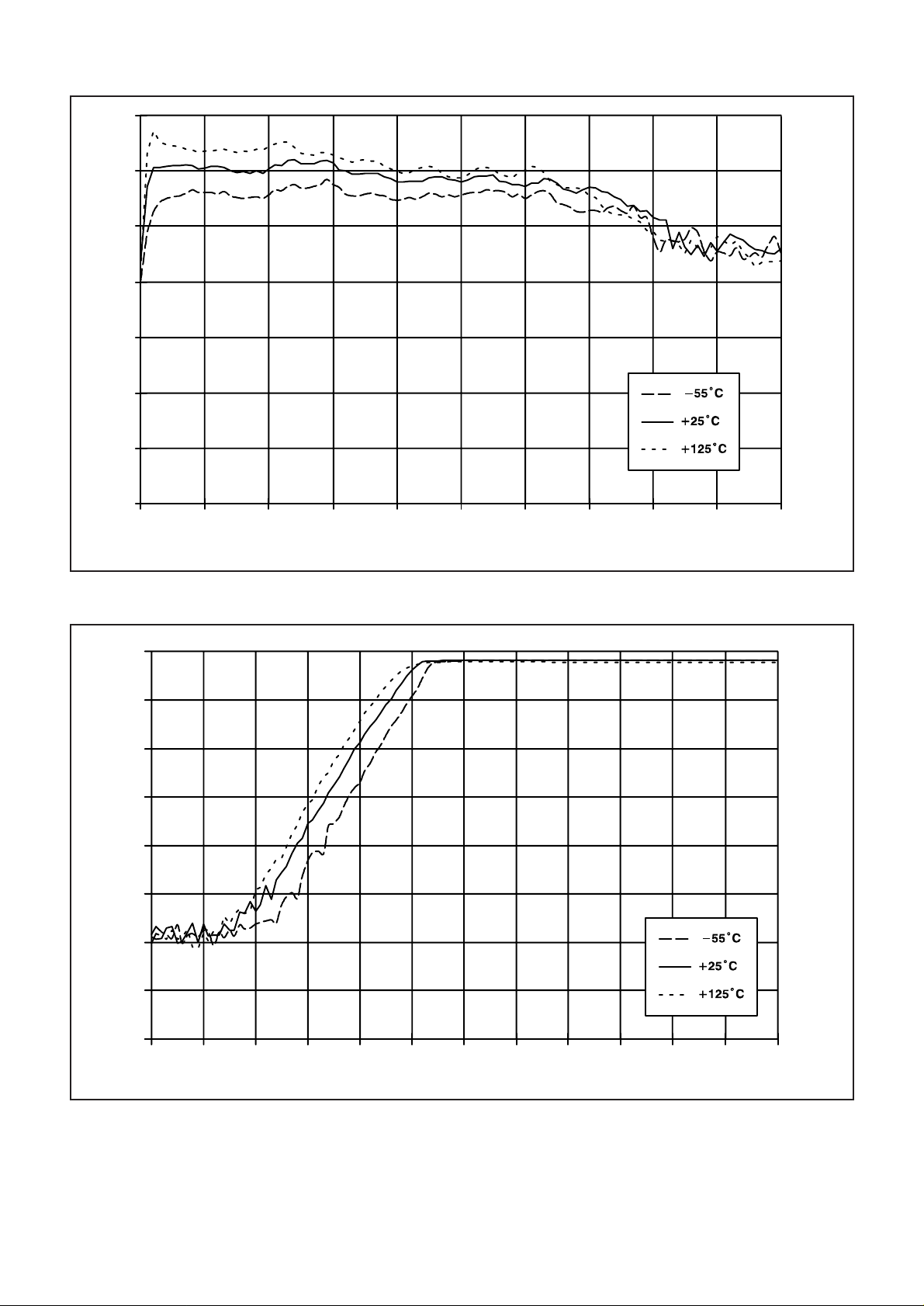
Fig.16 Linear gain (-70dBm I/P)
12
–40
–110 –100 –90 –80 –70 –60 –50 –40 –30 –20 –10 0 10
RF input power (dBm)
Fig.17 RF input → output limiting transfer characteristic at Frequency = 100MHz
Page 13
0
–5
–10
–15
–20
–25
RF output power (dBm)
–30
–35
SL3522
–40
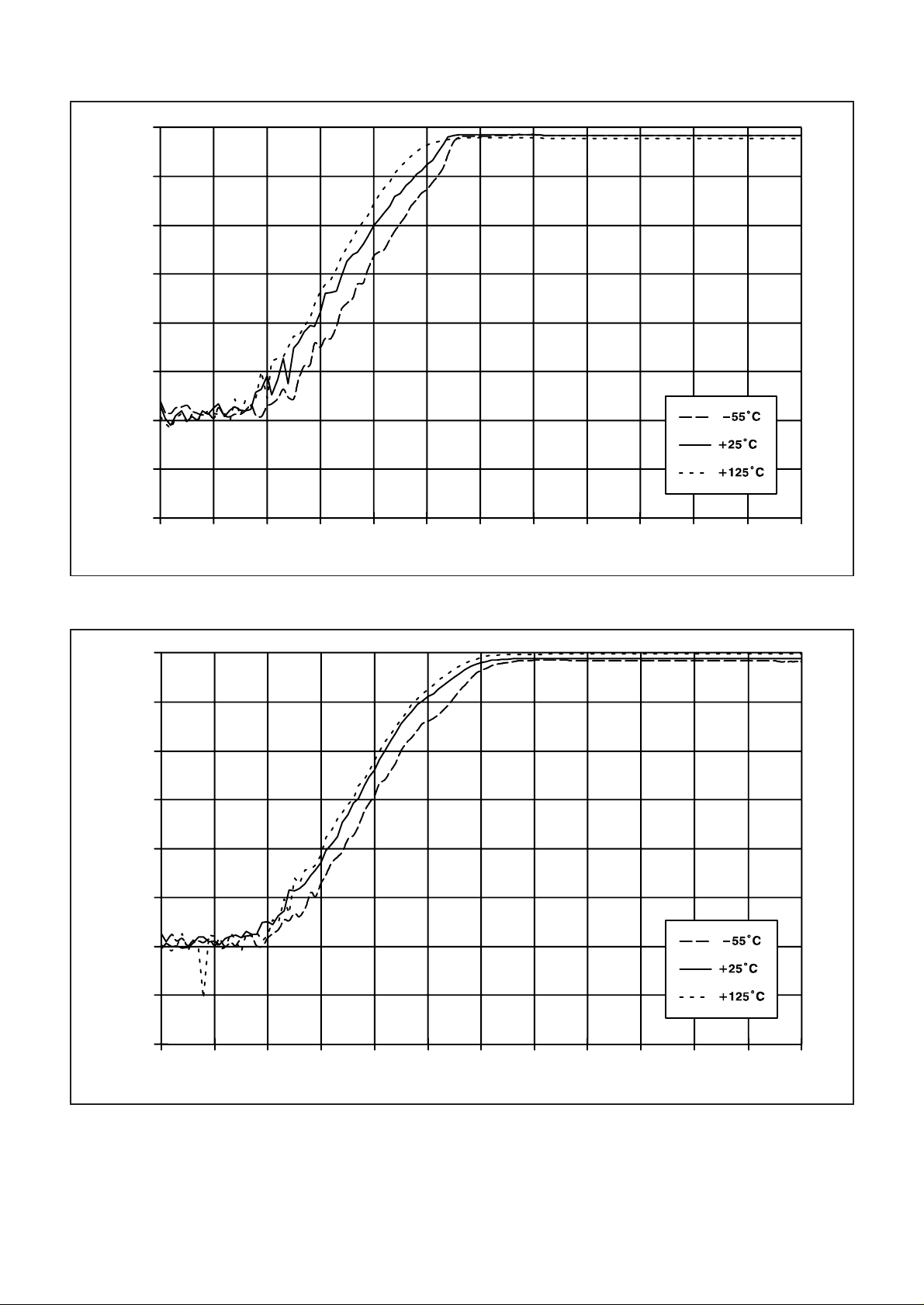
–110 –100 –90 –80 –70 –60 –50 –40 –30 –20 –10 0 10
RF input power (dBm)
Fig.18 RF input → output limiting transfer characteristic at Frequency = 325MHz
0
–5
–10
–15
–20
–25
RF output power (dBm)
–30
–35
–40
–110 –100 –90 –80 –70 –60 –50 –40 –30 –20 –10 0 10
RF input power (dBm)
Fig.19 RF input → output limiting transfer characteristic at Frequency = 500MHz
13
Page 14
SL3522
20
15
10
5
0
–5
Phase error (degrees)
–10
–15
–20
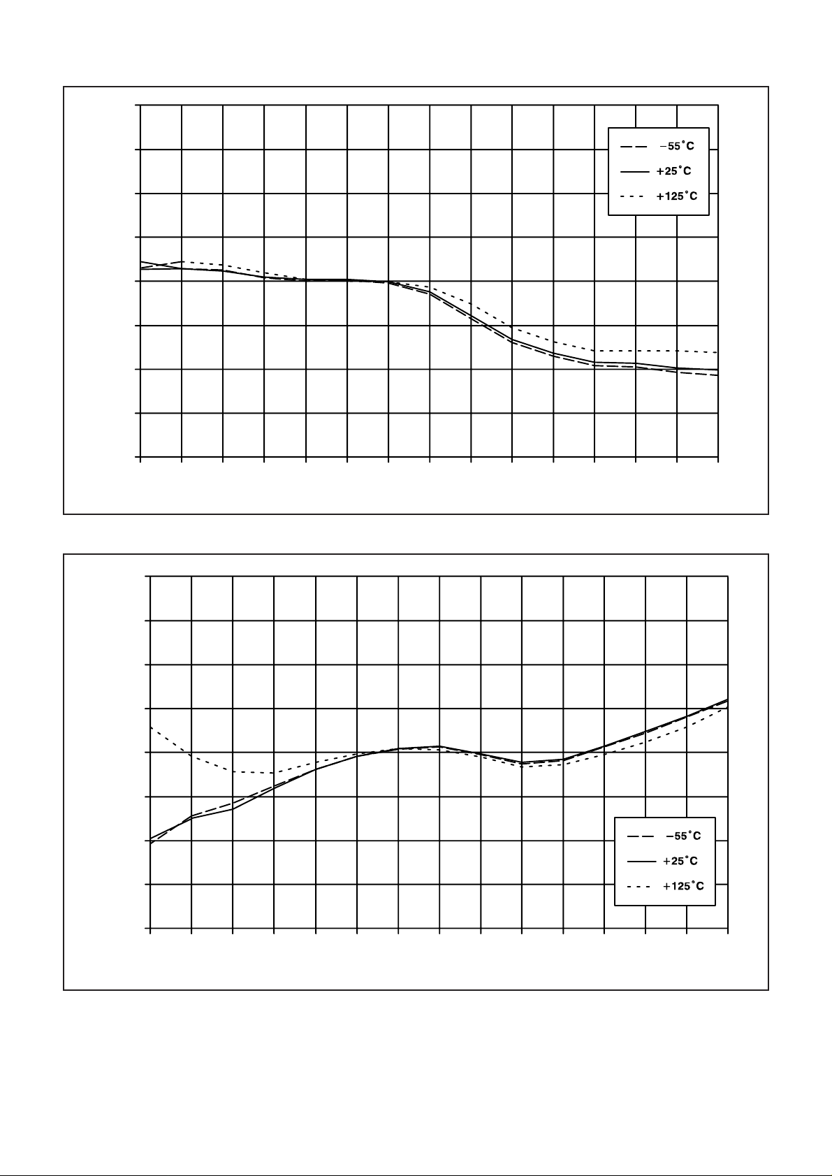
–60 –55 –50 –45 –40 –35 –30 –25 –20 –15 –10 –5 0 5 10
20
15
10
5
0
–5
Phase error (degrees)
–10
–15
RF input power (dBm)
Fig.20 Limiting phase (100MHz) normalised at -30dBm
14
–20
–60 –55 –50 –45 –40 –35 –30 –25 –20 –15 –10 –5 0 5 10
RF input power (dBm)
Fig.21 Limiting phase (300MHz) normalised at -30dBm
Page 15
20
15
10
5
0
–5
Phase error (degrees)
–10
–15
SL3522
–20
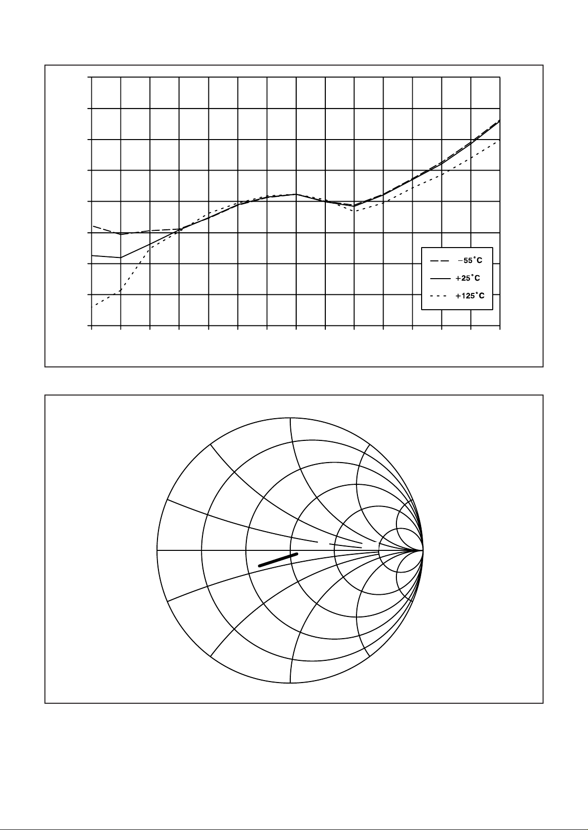
–60 –55 –50 –45 –40 –35 –30 –25 –20 –15 –10 –5 0 5 10
RF input power (dBm)
Fig.22 Limiting phase (500MHz) normalised at -30dBm
+j1
+j0.2
–j0.2
+j0.5
0.50.2 10
600MHz
2
100MHz
+j2
+j5
5
–j5
–j0.5
–j1
–j2
Fig.23 Typical input impedance normalised to 50Ω - 20dBm I/P level
15
Page 16
SL3522
9
10
5kR
–
OFFSETGAIN
13
500R
12
BUFFER
VIDEO O/P
+
16171819
–0.55V
LIMITING RF
OUTPUT BUFFER
8
21
50R 50R
STAGES 6&7
14
11
20
15
STAGE 4 STAGE 5
60 23
STAGE 3
2457 22
RF I/P +
RF I/P –
VEEGND
VEEGND
VEEGND
27262524232221201918171615
40 25
STAGE 1 STAGE 2
27
20pF
55R
20pF
326
25R
28
12823456789
EE
EE
EE
V
GND
GND
V
RF O/P GND
N/C
N/C
V
ADJUST
& OFFSET
VIDEO GAIN
VIDEO VEEGAIN ADJUST
TRIM REF
OFFSET ADJ
VIDEO GND
1011121314
EE
EE
RF O/P –
RF O/P +
VIDEO O/P
RF O/P V
VIDEO O/P V
CC
VIDEO V
CC
VIDEO O/P V
TO
RR
G
R
Fig.24 SL3522 Schematic diagram
16
Page 17
SL3522
1
46 45 44 43 42 41 40 39 38 37 36 35 34
2
3
4
56789101112
13 15 16 17 18 19 20 2114
33 32 31 30 29 28
47
48
49
50
51
52
27
26
25
24
23
22
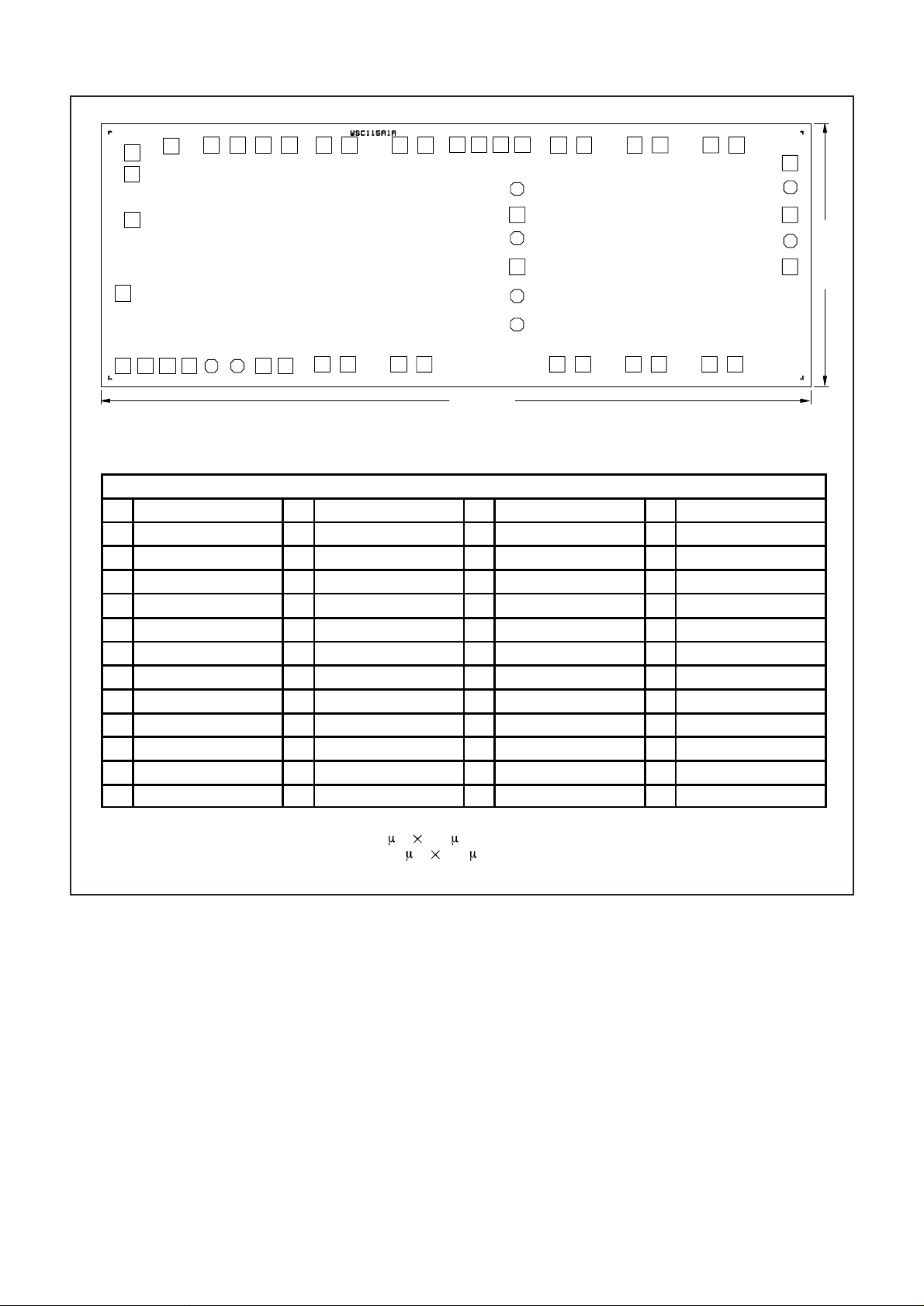
5.480mm
TO SCALE
TERMINALS ((X) DENOTES MC PACKAGE PIN NUMBER)
1 Video O/P (13) 14 VEE 5A (22) 27 Test point 40 VEE 5B (7)
2 Video O/P VCC (14) 15 VEE 4A (22) 28 VEE 1B (3) 41 RF BUF O/P GND (8)
3 Gain VCC (15) 16 GND 4B (23) 29 GND 1B (4) 42 RF BUF O/P GND (8)
4 Video GND (16) 17 GND 3A (23) 30 GND 2B (4) 43 RF O/P – (9)
5 Offset ADJ (17) 18 VEE 3A (24) 31 VEE 2A (5) 44 RF O/P + (10)
6 Trim REF (18) 19 VEE 2A (24) 32 VEE 3A (5) 45 RF BUF O/P VEE (11)
7 Gain ADJ (19) 20 GND 2A (25) 33 GND 3B (6) 46 Video O/P VEE (12)
8 Gain VEE (20) 21 GND 1A (25) 34 Test point 47 Test point
9 Test point 22 VEE 1A (26) 35 Test point 48 Test point
10 Test point 23 Test point 36 T est point 49 Test point
11 VEE 6A (20) 24 RF I/P signal (27) 37 Test point 50 Test point
12 GND 6A (21) 25 Test point 38 GND 4B (6) 51 Test point
13 GND 5A (21) 26 RF I/P return (28) 39 VEE 4B (7) 52 Test point
2.085mm
NOTES
1. All pads with square cross–section =120
2. All pads with octagonal cross–section =100
3. Chip is passivated with polyimide
Fig.25 SL3522 pad map for bare IC dice
m 120 m
m 100 m
17
Page 18
Page 19

http://www.mitelsemi.com
World Headquarters - Canada
Tel: +1 (613) 592 2122
Fax: +1 (613) 592 6909
North America Asia/Pacific Europe, Middle East,
Tel: +1 (770) 486 0194 Tel: +65 333 6193 and Africa (EMEA)
Fax: +1 (770) 631 8213 Fax: +65 333 6192 Tel: +44 (0) 1793 518528
Fax: +44 (0) 1793 518581
Information relating to products and services furnished herein by Mitel Corporation or its subsidiaries (collectively “Mitel”) is believed to be reliable. However, Mitel assumes no
liability for errors that may appear in this publication, or for liability otherwise arising from the application or use of any such information, product or service or for any infringement of
patents or other intellectual property rights owned by third parties which may result from such application or use. Neither the supply of such information or purchase of product or
service conveys any license, either express or implied, under patents or other intellectual property rights owned by Mitel or licensed from third parties by Mitel, whatsoever.
Purchasers of products are also hereby notified that the use of product in certain ways or in combination with Mitel, or non-Mitel furnished goods or services may infringe patents or
other intellectual property rights owned by Mitel.
This publication is issued to provide information only and (unless agreed by Mitel in writing) may not be used, applied or reproduced for any purpose nor form part of any order or
contract nor to be regarded as a representation relating to the products or services concerned. The products, their specifications, services and other information appearing in this
publication are subject to change by Mitel without notice. No warranty or guarantee express or implied is made regarding the capability, performance or suitability of any product or
service. Information concerning possible methods of use is provided as a guide only and does not constitute any guarantee that such methods of use will be satisfactory in a specific
piece of equipment. It is the user’s responsibility to fully determine the performance and suitability of any equipment using such information and to ensure that any publication or
data used is up to date and has not been superseded. Manufacturing does not necessarily include testing of all functions or parameters. These products are not suitable for use in
any medical products whose failure to perform may result in significant injury or death to the user. All products and materials are sold and services provided subject to Mitel’s
conditions of sale which are available on request.
M Mitel (design) and ST-BUS are registered trademarks of MITEL Corporation
Mitel Semiconductor is an ISO 9001 Registered Company
Copyright 1999 MITEL Corporation
All Rights Reserved
Printed in CANADA
TECHNICAL DOCUMENTATION - NOT FOR RESALE
 Loading...