

Datasheet Si3012-KS, Si3012-KT, Si3014-KS, Si3014-KT, Si3015-BS Datasheet (Silicon Laboratories)
...Page 1
Si3035
3.3 V FCC/JATE D
IRECT
A
CCESS
A
Features
Complete DAA includes the following:
!
3.3 V to 5 V Digital/Analog
Power Supplies
!
JATE Filter Option
!
86 dB Dynamic Range TX/RX
Paths
!
Daisy-Chaining for Up to Eight
Devices
!
Integrated Ring Detec t or
!
3000 V Isolation
!
Support for Caller ID
!
Low Profile SOIC Packages
!
Direct Interface to DSPs
!
Integrated Modem Codec
!
Compliant with FCC Part 68
!
Low-Power Standb y Mode
!
Proprietary ISOcap™ Technology
!
Pin Compatible with Si3034, Si3032
!
Optional IIR Digital Filter
Applications
!
V.90 Modems
!
Voice Mail Systems
!
Fax Machines
!
Set Top Boxes
Description
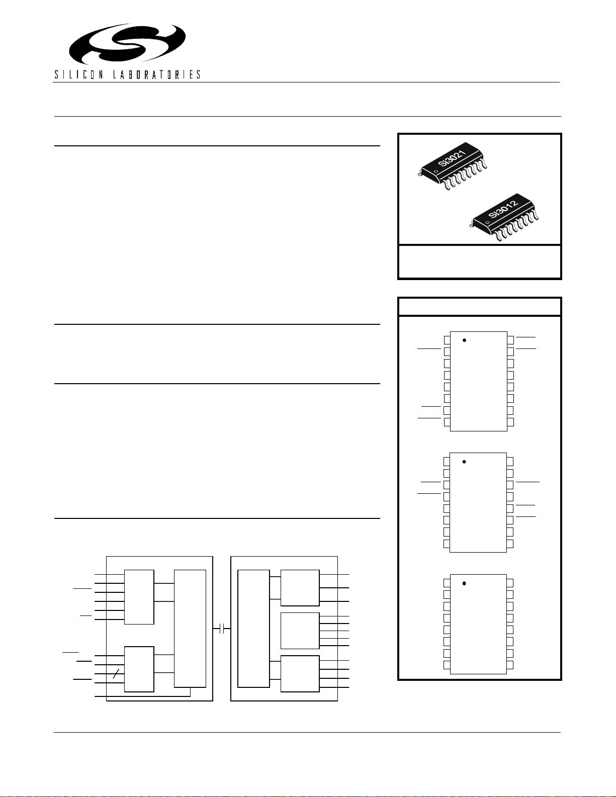
The Si3035 is an integrat ed direct ac cess arrange ment (DAA) c hipset that
provides a digital, low-cost, solid-state interface to a telephone line.
Available in two 16-pin small outline packages, it eliminates the need for an
analog front end (AFE), a n is olation transformer, relays, opto-isolators, and
a 2- to 4-wire hybrid. The Si3035 dramatically reduces the number of
discrete components and cost require d to achieve compliance with FCC
Part 68. The Si3035 interfaces directly to standard modem DSPs and
supports all FCC and J ATE out-of-band noise require ments. International
support is provided by the pin compatible Si3034.
Functional Block Diagram
Si3021 Si3012
RRANGEMENT
Ordering Information
See page 50.
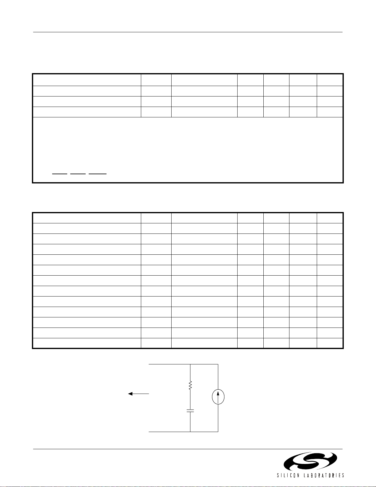
Pin Assignments
Si3021 (SOIC)
MCLK
FSYNC
SCLK
FC/RGDT
RESET
FC/RGDT
RESET
AOUT
1
2
3
V
4
D
SDO
5
SDI
6
7
8
Si3021 (TSSOP)
1
SDO
SDI
2
3
4
5
M1
6
C1A
7
GND
8
16
15
14
13
12
11
10
9
16
15
14
13
12
11
10
9
OFHK
RGDT/FSD
M0
V
A
GND
C1A
M1
AOUT
V
D
SCLK
FSYNC
MCLK
OFHK
RGDT/FSD
M0
V
A
MCLK
SCLK
FSYNC
SDI
SDO
FC/RGT
RGDT/FSD
OFHK
MODE
RESET
AOUT
Digital
Interfa ce
Control
Interfa ce
Isolation
Interfa ce
Isolation
Interfa ce
Hybrid
DC
Termination
Ring Detect
Off-H o o k
Out
TX
In
RX
HYBD
VREG2
VREG
DCT
REXT
IGND
RNG1
RNG2
QB
QE
Si3012 (SOIC or TSSOP)
TSTA
TSTB
IGND
RNG1
RNG2
C1B
QB
QE
1
2
3
4
5
6
7
8
US Patent # 5,870,046
TX
16
NC
15
RX
14
REXT
13
DCT
12
HYBD
11
VREG2
10
VREG
9
US Patent # 6,061,009
Other Patents Pending
Rev. 1.2 12/00 Copyright © 2000 by Silicon Laboratories Si3035-DS12
Page 2

Si3035
2 Rev. 1.2
Page 3

Si3035
T
ABLE OF
C
ONTENTS
Section Page
Electrical Specifications . . . . . . . . . . . . . . . . . . . . . . . . . . . . . . . . . . . . . . . . . . . . . . . . . 4
Typical Application Circuit . . . . . . . . . . . . . . . . . . . . . . . . . . . . . . . . . . . . . . . . . . . . . . . 15
Bill of Materials . . . . . . . . . . . . . . . . . . . . . . . . . . . . . . . . . . . . . . . . . . . . . . . . . . . . . . 16
Analog Output . . . . . . . . . . . . . . . . . . . . . . . . . . . . . . . . . . . . . . . . . . . . . . . . . . . . . . 17
Functional Description . . . . . . . . . . . . . . . . . . . . . . . . . . . . . . . . . . . . . . . . . . . . . . . . . . 18
Initialization . . . . . . . . . . . . . . . . . . . . . . . . . . . . . . . . . . . . . . . . . . . . . . . . . . . . . . . . 18
Isolation Barrier . . . . . . . . . . . . . . . . . . . . . . . . . . . . . . . . . . . . . . . . . . . . . . . . . . . . . 18
Off-Hook . . . . . . . . . . . . . . . . . . . . . . . . . . . . . . . . . . . . . . . . . . . . . . . . . . . . . . . . . . . 18
Ring Detect . . . . . . . . . . . . . . . . . . . . . . . . . . . . . . . . . . . . . . . . . . . . . . . . . . . . . . . . 19
Improved JATE Support . . . . . . . . . . . . . . . . . . . . . . . . . . . . . . . . . . . . . . . . . . . . . . . 19
Digital Interface . . . . . . . . . . . . . . . . . . . . . . . . . . . . . . . . . . . . . . . . . . . . . . . . . . . . . 19
Clock Generation Subsystem . . . . . . . . . . . . . . . . . . . . . . . . . . . . . . . . . . . . . . . . . . . 20
Power Management . . . . . . . . . . . . . . . . . . . . . . . . . . . . . . . . . . . . . . . . . . . . . . . . . . 24
Analog Output . . . . . . . . . . . . . . . . . . . . . . . . . . . . . . . . . . . . . . . . . . . . . . . . . . . . . . 24
On-Hook Line Monitor . . . . . . . . . . . . . . . . . . . . . . . . . . . . . . . . . . . . . . . . . . . . . . . . 25
Loop Current Monitor . . . . . . . . . . . . . . . . . . . . . . . . . . . . . . . . . . . . . . . . . . . . . . . . . 25
Multiple Device Support . . . . . . . . . . . . . . . . . . . . . . . . . . . . . . . . . . . . . . . . . . . . . . . 25
Gain Control . . . . . . . . . . . . . . . . . . . . . . . . . . . . . . . . . . . . . . . . . . . . . . . . . . . . . . . . 26
Filter Selection . . . . . . . . . . . . . . . . . . . . . . . . . . . . . . . . . . . . . . . . . . . . . . . . . . . . . . 26
Revision Identification . . . . . . . . . . . . . . . . . . . . . . . . . . . . . . . . . . . . . . . . . . . . . . . . 32
Calibration . . . . . . . . . . . . . . . . . . . . . . . . . . . . . . . . . . . . . . . . . . . . . . . . . . . . . . . . . 32
In-Circuit Testing . . . . . . . . . . . . . . . . . . . . . . . . . . . . . . . . . . . . . . . . . . . . . . . . . . . . 32
Exception Handling . . . . . . . . . . . . . . . . . . . . . . . . . . . . . . . . . . . . . . . . . . . . . . . . . . 33
Control Registers . . . . . . . . . . . . . . . . . . . . . . . . . . . . . . . . . . . . . . . . . . . . . . . . . . . . . . . 34
Appendix—UL1950 3rd Edition . . . . . . . . . . . . . . . . . . . . . . . . . . . . . . . . . . . . . . . . . . . . 45
Pin Descriptions: Si3021 . . . . . . . . . . . . . . . . . . . . . . . . . . . . . . . . . . . . . . . . . . . . . . . . . 46
Pin Descriptions: Si3012 . . . . . . . . . . . . . . . . . . . . . . . . . . . . . . . . . . . . . . . . . . . . . . . . . 48
Ordering Guide . . . . . . . . . . . . . . . . . . . . . . . . . . . . . . . . . . . . . . . . . . . . . . . . . . . . . . . . . 50
SOIC Outline . . . . . . . . . . . . . . . . . . . . . . . . . . . . . . . . . . . . . . . . . . . . . . . . . . . . . . . . . . . 51
TSSOP Outline . . . . . . . . . . . . . . . . . . . . . . . . . . . . . . . . . . . . . . . . . . . . . . . . . . . . . . . . . 52
Contact Information . . . . . . . . . . . . . . . . . . . . . . . . . . . . . . . . . . . . . . . . . . . . . . . . . . . . . 54
Rev. 1.2 3
Page 4
Si3035
Electrical Specifications
Table 1. Recommended Operating Conditions
Parameter
1
Ambient Temperature T
Si3021 Supply Voltage, Analog V
Si3021 Supply Voltage, Digital
Notes:
1.
The Si3035 specifications are guaranteed when the typical application circuit (including component
3
Symbol Test Condition
A
A
V
D
K-Grade 0 25 70 °C
Min
2
Typ
Max
2
Unit
4.75 5.0 5.25 V
3.0 3.3/5.0 5.25 V
tolerances) and any Si3021 and any Si3012 are used. See Figure 16 on page 15 for typical application
circuit.
2.
All minimum and maximum specifications are guaranteed and apply across the recommended operating conditions.
Typical values apply at nominal supply voltages and an operating temperature of 25 °C unless otherwise stated.
3. The digital supply, V
operating from 3.3 V. The 3.3 V operation applies to both the serial port and the digital signals
RGDT, OFHK, RESET, M0, and M1.
, can operate from either 3.3 V or 5.0 V. The Si3021 supports interface to 3.3 V logic when
D
Table 2. Loop Characteristics
(VA = Charge Pump, VD = +3.3 V ± 0. 3 V, TA = 0 to 70°C for K-Grade, Refer to Figure 1)
Parameter Symbol Test Condition Min Typ Max Unit
DC Termination Voltage V
DC Termination Voltage V
DC Ring Current (
DC Ring Current
with caller ID)
(w/o caller ID)
AC Termination Impedance Z
Operating Loop Current I
I
RDC
I
RDC
ACT
LP
TR
TR
Loop Current Sense Bits LCS LCS = Fh 180 155 — mA
IL = 20 mA — — 7.7 V
IL = 105 mA 12 — — V
—— 1 mA
—— 20µA
—600— Ω
20 — 120 mA
Ring Voltage Detect V
Ring Frequency F
On-Hook Leakage Current I
Ringer Equivalence Num. (
Ringer Equivalence Num.
with caller ID)
(w/o caller ID)
Si3012
RING
RD
R
LK
V
BAT
REN — 1.0 1.67 —
REN — 0.2 — —
TIP
+
600
Ω
V
TR
10 µF
–
Figure 1. Test Circuit for Loop Characteristics
4 Rev. 1.2
13 18 26 V
RMS
15 — 68 Hz
= –48 V — — 1 µA
I
L
Page 5
Si3035
Table 3. DC Characteristics, VD = +5 V
(VA = +5 V ±5%, VD = +5 V ±5%, TA = 0 to 70°C for K-Grade)
Parameter Symbol Test Condition Min Typ Max Unit
High Level Input Voltage V
Low Level Input Voltage V
High Level Output Voltage V
Low Level Output Voltage V
Input Leakage Current I
Power Supply Current, Analog I
Power Supply Current, Digital
Total Supply Current, Sleep Mode
Total Supply Current, Deep Sleep
Notes:
1. All inputs at 0.4 or V
= 0 mA).
OUT
is not functional in this state.
2.
(Static I
RGDT
1
1
1,2
– 0.4 (CMOS levels). All inputs held static except clock and all outputs unloaded
D
IA + I
IA + I
OH
OL
I
D
IH
IL
IO = –2 mA 3.5 — — V
IO = 2 mA — — 0.4 V
L
A
VA pin — 0.3 1 mA
VD pin — 14 18 mA
D
D
PDN = 1, PDL = 0 — 1.3 2.5 mA
PDN = 1, PDL = 1 — 0.04 0.5 mA
3.5 — — V
——0.8V
–10 — 10 µA
Table 4. DC Characteristics, VD = +3.3 V
(VA = Charge Pump, VD = +3.3 V ± 0.3 V, TA = 0 to 70°C for K-Grade)
Parameter Symbol Test Condition Min Typ Max Unit
High Level Input Voltage V
Low Level Input Voltage V
High Level Output Voltage V
Low Level Output Voltage V
Input Leakage Current I
Power Supply Current, Analog
Power Supply Current, Digital
Total Supply Current, Sleep Mode
Total Supply Current, Deep Sleep
Power Supply Voltage, Analog
Notes:
1. Only a decoupling capacitor should be connected to V
2. There is no I
to the V
3. All inputs at 0.4 or V
(Static I
4. RGDT
5. The charge pump is rec om m end ed to be used only when V
applied to the device before V
current consumption when the internal charge pump is enabled and only a decoupling cap is connected
A
pin.
A
= 0 mA).
OUT
is not functional in this state.
1,2
3
3
3,4
1,5
– 0.4 (CMOS levels). All inputs held static except clock and all outputs unloaded
D
is applied on power up if driven from separate supplies.
D
IH
IL
OH
OL
L
I
A
I
D
IA + I
IA + I
V
D
D
A
2.0 — — V
——0.8V
IO = –2 mA 2.4 — — V
IO = 2 mA — — 0.35 V
–10 — 10 µA
VA pin — 0.3 1 mA
VD pin — 9 12 mA
PDN = 1, PDL = 0 — 1.2 2.5 mA
PDN = 1, PDL = 1 — 0.04 0.5
Charge Pump On 4.3 4.6 5.00 V
when the charge pump is on.
A
< 4.5 V. When the charge pum p is not use d, VA should be
D
Rev. 1.2 5
Page 6

Si3035
Table 5. AC Characteristics
(VA = Charge Pump, VD = +3.3 V ± 0.3 V, TA = 0 to 70°C for K-Grade)
Parameter Symbol Test Condition Min Typ Max Unit
Sample Rate
1
PLL1 Output Clock Frequency F
Transmit Frequency Response Low –3 dB corner — 16 — Hz
Receive Frequency Response Low –3 dB corner — 16 — Hz
2
Transmit Full Scale Level
Receive Full Scale Level
Dynamic Range
Dynamic Range
4
5
Total Harmonic Distortion
(0 dB gain) V
2,3
(0 dB gain) V
6
Fs Fs = F
PLL1
FPLL1 = F
TX
RX
/5120 7.2 — 11.025 kHz
PLL2
"
MCLK
M1/N1 36 — 58 MHz
—0.98—V
—0.98—V
PEAK
PEAK
DR VIN = 1 kHz, –3 dBFS 80 86 — dB
DR VIN = 1 kHz, –3 dBFS — 84 — dB
THD VIN = 1 kHz, –3 dBFS — –84 — dB
Dynamic Range (call progress AOUT) DR
THD (call progress AOUT) THD
AO
AO
AOUT Full Scale Level — 0.75 V
VIN = 1 kHz 60 — — dB
VIN = 1 kHz — 1.0 — %
—V
D
PP
AOUT Output Impedance — 10 — kΩ
Mute Level (call progress AOUT) –90 — — dB
Dynamic Range (caller ID mode) DR
Caller ID Full Scale Level (0 dB gain)
Notes:
1. See Figure 23 on page 22.
2. Parameter measured at TIP and RING of Figure16 on page 15.
3. Receive Full Scale Level will produce – 0.9 dBFS at SDO.
4.
DR = 3 dB + 20 log (RMS signal/RMS noise). Applies to both the transmit and receive paths. Measurement bandwidth
is 300 to 3400 Hz. Sample Rate = 9.6 kHz, Loop Current = 40 mA.
5.
DR = 3 dB + 20 log (RMS signal/RMS noise). Applies to both the transmit and receive paths. Measurement bandwidth
is 15 to 3400 Hz. Sample Rate = 9.6 kHz, Loop Current = 40 mA.
6. THD = 20 log (RMS distortion/RMS signal). Applies to both the transmit and receive paths.
Sample Rate = 9.6 kHz, Loop Current = 40 mA.
2
V
CID
VIN = 1 kHz, –13 dBFS — 60 — dB
CID
—0.8—V
PEAK
6 Rev. 1.2
Page 7
Si3035
Table 6. Absolute Maximum Ratings
Parameter Symbol Value Unit
DC Supply Voltage V
Input Current, Si3021 Digital Input Pins I
Digital Input Voltage V
Operating Temperature Range T
Storage Temperature Range T
Note: Permanent device damage may occur if the above Absolute Maximum Ratings are exceeded. Functional operation
should be restricted to the conditions as specified in the operational sections of this data sheet. Exposure to absolute
maximum rating conditions for extended periods may affect device reliability.
, V
D
IN
IND
STG
A
–0.5 to 6.0 V
±10 mA
–0.3 to (VD + 0.3) V
A
–40 to 100 °C
–65 to 150 °C
Table 7. Switching Characteristics—General Inputs
(VA = Charge Pump, VD = 3.0 to 5.25 V, TA = 0 to 70°C for K-Grade, CL = 20 pF)
Parameter
1
Cycle Time, MCLK t
MCLK Duty Cycle t
Rise Time, MCLK t
Fall Time, MCLK t
MCLK Before RESET
RESET
Pulse Width
M0, M1 Before RESET
Notes:
1.
All timing (except Rise and Fall time) is referenced to the 50% level of the waveform. Input test levels are
VIH = VD – 0.4 V, VIL = 0.4 V. Rise and Fall times are referenced to the 20% and 80% levels of the waveform.
2. The minimum RESET
3. M0 and M1 are typically connected to V
↑ t
2
3
↑
pulse width is the greater of 250 ns or 10 MCLK cycle times.
or GND and should not be changed during normal operation.
D
Symbol Min Typ Max Unit
16.67 — 1000 ns
40 50 60 %
—— 5 ns
—— 5 ns
10 — — cycles
250 — — ns
150 — — ns
t
mc
dty
mr
t
rl
mxr
r
f
MCLK
RESET
M0, M1
t
t
r
t
rl
t
mxr
mc
t
mr
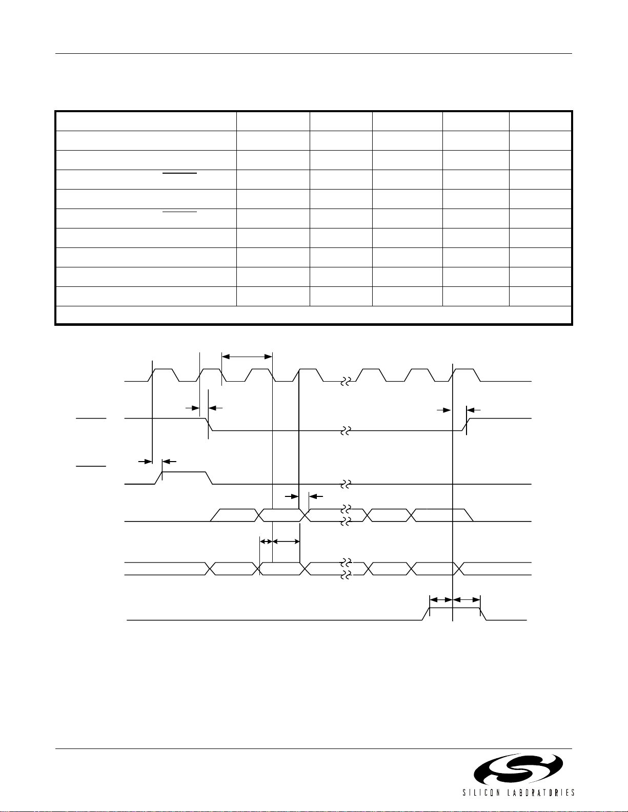
Figure 2. General Inputs Timing Diagram
Rev. 1.2 7
t
f
V
IH
V
IL
Page 8
Si3035
Table 8. Switching Characteristics—Serial Int erface (DCE = 0)
(VA = Charge Pump, VD = 3.0 to 5.25 V, TA = 0 to 70°C for K-Grade, CL = 20 pF)
Parameter Symbol Min Typ Max Unit
Cycle time, SCLK t
SCLK duty cy cle t
Delay time, SCLK ↑ to FSYNC
↓ t
Delay time, SCLK ↑ to SDO valid t
Delay time, SCLK ↑ to FSYNC
↑ t
Setup time, SDI before SCLK ↓ t
Hold time, SDI after SCLK ↓ t
Setup time, FC ↑ before SCLK ↑ t
Hold time, FC ↑ after SCLK ↑ t
c
dty
d1
d2
d3
su
h
sfc
hfc
354 1/256 Fs — ns
—50—%
——10ns
——20ns
——10ns
25 — — ns
20 — — ns
40 — — ns
40 — — ns
Note: All timing is referenced to the 50% level of the waveform. Input test levels are V
t
c
SCLK
t
d1
FSYNC
(mode 0)
= VD – 0.4 V, VIL = 0.4 V
IH
t
d3
V
OH
V
OL
FSYNC
(mode 1)
16 Bit
SDO
16 Bit
SDI
FC
t
d3
t
d2
D15 D14 D1 D0
t
su
t
h
Figure 3. Serial Interface Timing Diagr am
D0D1D14D15
t
sfc
t
hfc
8 Rev. 1.2
Page 9

Table 9. Switching Characteristics—Serial Int erface (DCE = 1, FSD = 0)
(VA = Charge Pump, VD = 3.0 to 5.25 V, TA = 0 to 70°C for K-Grade, CL = 20 pF)
Si3035
Parameter
1,2
Cycle Time, SCLK t
SCLK Duty Cycle t
Delay Time, SCLK ↑ to FSYNC
Delay Time, SCLK ↑ to FSYNC
↑ t
↓ t
Delay Time, SCLK ↑ to SDO valid t
Delay Time, SCLK ↑ to SDO Hi-Z t
Delay Time, SCLK ↑ to RGDT
Delay Time, SCLK ↑ to RGDT
↓ t
↑ t
Setup Time, SDO Before SCLK ↓ t
Hold Time, SDO After SCLK ↓ t
Setup Time, SDI Before SCLK t
Hold Time, SDI After SCLK t
Symbol Min Typ Max Unit
c
dty
d1
d2
d3
d4
d5
d6
su
h
su2
h2
354 1/256 Fs — ns
—50 —%
— — 10 ns
— — 10 ns
0.25tc – 20 — 0.25tc + 20 ns
— — 20 ns
— — 20 ns
— — 20 ns
25 — — ns
20 — — ns
25 — — ns
20 — — ns
Notes:
1. All timing is referenced to the 50% level of the waveform. Input test levels are V
2. Refer to the section "Multiple Device Support" on page 25 for functional details.
32 SCLKs
t
c
16 SCLKs 16 SCLKs
= VD – 0.4 V, VIL = 0.4 V.
IH
SCLK
t
d1
FSYNC
(mode 1)
FSYNC
(mode 0)
t
SDO
(ma ster)
SDO
(slave 1)
FSD
(Mode 0)
FSD
(Mode 1)
SDI D15 D0
t
d2
t
d5
d3
t
su
D15 D14 D13 D0
t
su2
D14
t
h
t
h2
D13
t
d2
t
d6
t
d4
t
d5
t
d3
D15
t
d5
t
d2
Figure 4. Serial Interface Timing Diagram (DCE = 1, FSD = 0)
Rev. 1.2 9
Page 10

Si3035
Table 10. Switching Characteristics—Serial Interface (DCE = 1, FSD = 1)
(VA = Charge Pump, VD = 3.0 to 5.25 V, TA = 0 to 70°C for K-Grade, CL = 20 pF)
Parameter
1,2
Cycle Time, SCLK t
SCLK Duty Cycle t
Delay Time, SCLK ↑ to FSYNC
Delay Time, SCLK ↑ to FSYNC
↑ t
↓ t
Delay Time, SCLK ↑ to SDO valid t
Delay Time, SCLK ↑ to SDO Hi-Z t
Delay Time, SCLK ↑ to RGDT
↓ t
Setup Time, SDO Before SCLK ↓ t
Hold Time, SDO After SCLK ↓ t
Setup Time, SDI Before SCLK t
Hold Time, SDI After SCLK t
Symbol Min Typ Max Unit
c
dty
d1
d2
d3
d4
d5
su
h
su2
h2
354 1/256 Fs — ns
—50 —%
— — 10 ns
— — 10 ns
0.25tc – 20 — 0.25tc + 20 ns
— — 20 ns
— — 20 ns
25 — — ns
20 — — ns
25 — — ns
20 — — ns
Notes:
1. All timing is referenced to the 50% level of the waveform. Input test levels are V
2. Refer to the section "Multiple Device Support" on page 25 for functional details.
= VD – 0.4 V, VIL = 0.4 V.
IH
SCLK
FSYNC
(mode 1)
SDO
(ma ste r)
SDO
(slave 1)
FSD
SDI
t
c
t
d1
t
d3
t
d2
D15
t
su
t
h
D14 D13 D0
t
d4
t
d3
D15
t
d5
D14
t
h2
t
su2
D15 D1 D0
Figure 5. Serial Interface Timing Diagram (DCE = 1, FSD = 1)
10 Rev. 1.2
Page 11
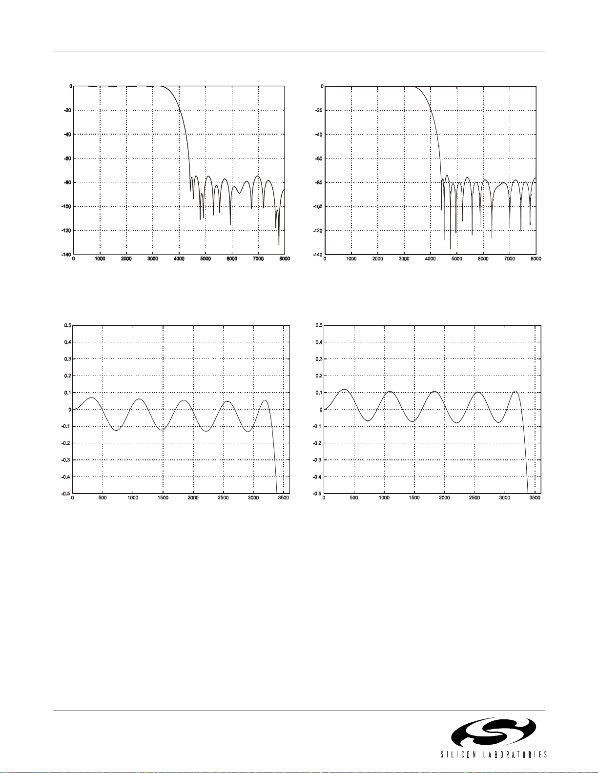
Table 11. Digital FIR Filter Characteristics—Transmit and Receive
(VA = Charge Pump, VD = +5 V ±5%, Sample Rate = 8kHz, TA = 0 to 70°C for K-Grade)
Parameter Symbol Min Typ Max Unit
Si3035
Passband (0.1 dB)
Passband (3 dB)
F
(0.1 dB)
F
(3 dB)
0—3.3kHz
0—3.6kHz
Passband Ripple Peak-to-Peak –0.1 — 0.1 dB
Stopband — 4.4 — kHz
Stopband Attenuation –74 — — dB
Group Delay
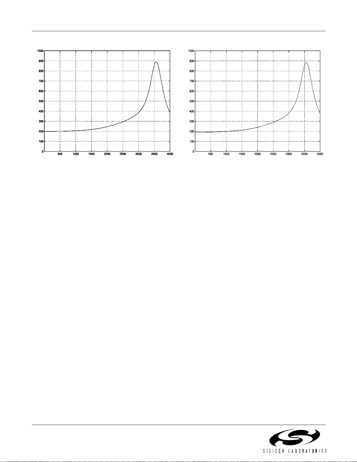
Note: Typical FIR filter characteristics for Fs = 8000 Hz are shown in Figures 6, 7, 8, and 9.
t
gd
— 12/Fs — sec
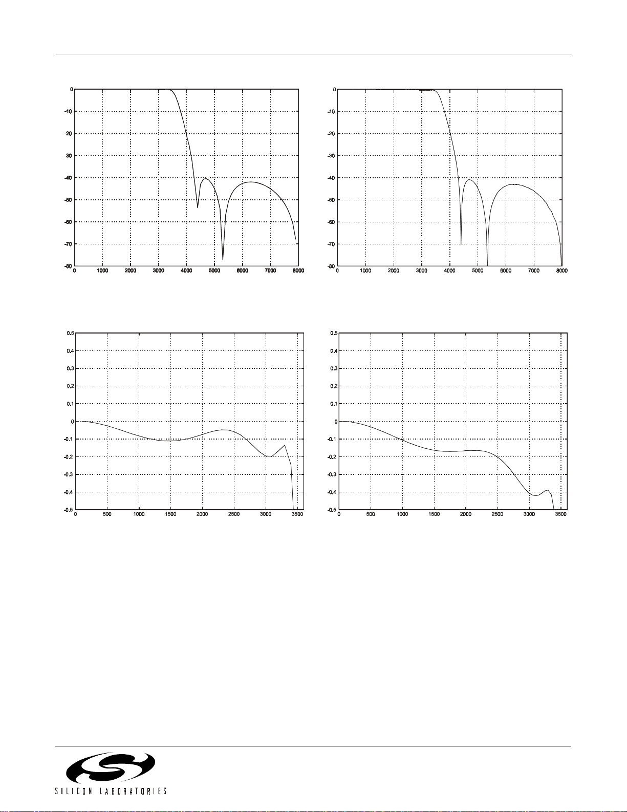
Table 12. Digital IIR Filter Characteri stics—Transmit and Receive
(VA = Charge Pump, VD = +5 V ±5%, Sample Rate = 8 kHz, TA = 0 to 70°C for K-Grade)
Parameter Symbol Min Typ Max Unit
Passband (3 dB)
F
(3 dB)
Passband Ripple Peak-to-Peak –0.2 — 0.2 dB
Stopband — 4.4 — kHz
Stopband Attenuation –40 — — dB
Group Delay
Note: Typical IIR filter characteristics for Fs = 8000 Hz are shown in Figures 10, 11, 12, and 13. Figures 14 and 15 show
group delay versus input frequency.
t
gd
0—3.6kHz
— 1.6/Fs — sec
Rev. 1.2 11
Page 12
Si3035
Attenuation—dB
Input Frequency—Hz
Figure 6. FIR Receive Filter Response
Attenuation—dB
Attenuation—dB
Input Frequency—Hz
Figure 8. FIR Transmit Filter Response
Attenuation—dB
Input Frequency—Hz
Figure 7. FIR Receive Filter Passband Ripple
For Figures 6–9, all filter plots apply to a sample rate of
Fs = 8 kHz. The filters scale with the sample rate as follows:
F
where Fs is the sample frequency.
12 Rev. 1.2
(0.1 dB)
F
(– 3 dB)
= 0.4125 Fs
= 0.45 Fs
Input Frequency—Hz
Figure 9. FIR T ransmi t Filter Passband Ripple
Page 13
Si3035
Attenuation—dB
Input Frequency—Hz
Figure 10. IIR Receive Filter Response
Attenuation—dB
Attenuation—dB
Input Frequency—Hz
Figure 12. IIR T ransmit Filter Response
Attenuation—dB
Input Frequency—Hz
Figure 11. IIR Receive Filter Passband Ripple
For Figures 10–13, all filter plots apply to a sample rate of
Fs = 8 kHz. The filters scale with the sample rate as follows:
F
(–3 dB)
where Fs is the sample frequency.
Input Frequency—Hz
Figure 13. IIR Transmit Filter Passband Ripple
= 0.45 Fs
Rev. 1.2 13
Page 14
Si3035
Delay—µs
Input Frequency—Hz
Figure 14. IIR Receive Group Delay Figure 15. IIR Transmit Group Delay
Delay—µs
Input Frequency—Hz
14 Rev. 1.2
Page 15

Typical Application Circuit
p
Decoupling cap for U1 VD
VCC
C10
RGDTb
OFHKb
MCLK
FSYNCb
SCLK
SDO
RESETb
AOUT
M0
SDI
FC
M1
R3
Decoupling cap for U1 VA
10
C3
Z4
U1
1
MCLK
2
FSYNC
3
SCLK
4
VD
5
SDO
6
SDI
7
FC
89
RESET AOUT
SOIC Pinout
Si3021
OFHK
RGDT
GND
16
15
14
M0
13
VA
12
11
C1A
10
M1
D3
BAV99
R27
C30
Rev. 1.2 15
No Ground Plane In DAA Section
R28
C1
D4
BAV99
C2
Z5
U2
Si3012
1
2
3
4
5
6
7
89
TSTA
TSTB
NC2
IGND
C1B
REXT
RNG1
DCT
RNG2
HYBD
QB
VREG2
QE VREG
16
TX
15
14
RX
13
12
11
10
C6
C16
R23
R1
R4
C12
R2
C8
R21
+
C5
C23
+
R18
Z1
R10
Q1
R5
Q2
R6
C20
Q3
FB2
RING
Note 1: R3 is not required when Vcc=3.3 V and the charge pump is
enabled (CPE = 1).
Note 2: If JATE support is not required, R21, C12 and C23
may be removed (R21 is effectively 0 ohms) and R4 should
be changed to a 604 ohm, 1/4 W, +- 1%.
Note 3: See Appendix for applications requiring UL 1950
3rd Edition com
liance.
D2
C9
C11
R22
C4
C7
R9
RV2
D1
C25
RV1
C24
FB1
C32
C31
TIP
Si3035
Figure 16. Typical Application Schematic
Page 16

Si3035
Bill of Materials
Table 13. Component Values—Typical Application
Component
1
Value Supplier(s)
C1,C4 150 pF, 3 kV, X7R, ±20% Novacap, Venkel, Johanson, Murata,
Panasonic, SMEC
C2 Not Installed
C3 0.22 µF, 16 V, X7R, ±20%
C5 1 µF, 16 V, Tant/Elec, ±20%
C6,C10,C16 0.1 µF, 16 V, X7R, ±20%
C7,C8,C9 15 nF, 250 V, X7R, ±20% Novacap, Johanson, Murata, Panasonic, SMEC
C11 39 nF, 16 V, X7R, ±20%
2
C12
2
C23
C24, C25, C31,C32
4
C30
5
D1,D2
3
2.7 nF, 16 V, X7R, ±20%
0.1 µF, 16 V, Tant/Elec/X7R, ±20%
1000 pF, 3 kV, X7R, ±10% Novacap, Venkel, Johanson, Murata, Panasonic, SMEC
Not Installed
Dual Diode, 300 V, 225 mA Central Semiconductor
D3,D4 BAV99 Dual Diode, 70 V, 350 mW Diodes, Inc., OnSemiconductor, Fairchild
FB1,FB2 Ferrite B ead Murata
Q1,Q3 A42, NPN, 300 V OnSemiconductor, Fairchild
Q2 A92, NPN, 300 V OnSemiconductor, Fairchild
RV1 Sidactor, 275 V, 100 A Teccor, ST Microelectronics, Microsemi, TI
RV2 MOV, 240 V Panasonic
R1 51 Ω, 1/2 W ±5%
R2 15 Ω, 1/4 W ±5%
R4
2
6
R3
,R18,R21
2
Not Installed
301 Ω, 1/10 W, ±1%
R5,R6 36 kΩ, 1/10 W ±5%
R9,R10 2 kΩ, 1/10 W ±5%
R22,R23 20 kΩ, 1/10 W ±5%
R27,R28 10 Ω, 1/10 W ±5%
U1 Si3021 Silicon Labs
U2 Si3012 Silicon Labs
Z1 Zener diode , 18 V Vishay, Rohm, OnSemiconductor
Z4,Z5 Zener diode, 5.6 V, 1/2 W Diodes, Inc., OnSemiconductor, Fairchild
Notes:
1. The following reference designators were intentionally omitted: C13–C15, C17–C22, C26–C29, R7, R8, R11–R17,
R19, and R20.
2. If JATE support is not required, C12, and C23 may be removed.
3.
Alternate population option is C24, C25 (2200 pF, 3 kV, X7R, ±10% and C31, C32 not installed).
4. Install only if needed for improved radiated emissions performance (10 pF, 16 V, NPO, ±10%).
5. Several diode bridge configurations are acc ep tab le (sup pl iers incl ude General Semi, Diodes Inc.)
6. If the charge pump is not enabl ed (with th e CPE bit in Register 6), V
a 10 Ω, 1/10 W, ±5% if V
is also 4.75 to 5.25 V.
D
must be 4.75 to 5.25 V. R3 can be installed with
A
16 Rev. 1.2
Page 17
Si3035
Analog Output
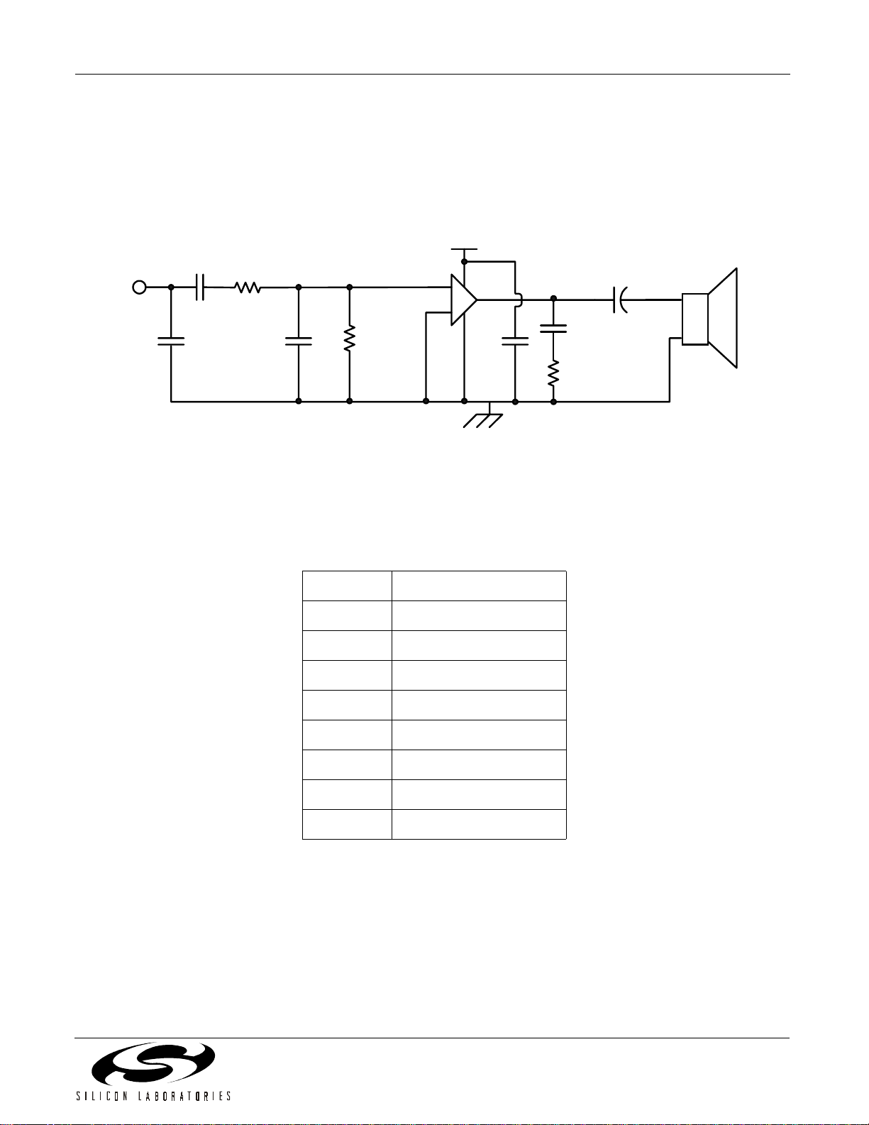
Figure 17 illustrates an optional application circuit to support the analo g output capability of the Si3035 for call
progress monitoring purp oses . T he AR M bi ts in Regi s ter 6 allow the receive path to be atte nua ted by 0 dB, –6 dB,
or –12 dB. The ATM bits, which are also in Register 6, allow the transmit path to be attenuated by –20 dB, –26 dB,
or –32 dB. Both the transmit and receive paths can also be independently muted.
+5 V
AOUT
C2
C1
R3
C6 R1
6
3
+
5
2
–
4
C3
R2
C4
+
C5
Speaker
Figure 17. Optional Connection to AOUT for a Call Progress Speaker
‘
Table 14. Component Values—Optional Connection to AOUT
Symbol Value
C1 2200 pF, 16 V, ±20%
C2, C3, C5 0.1 µF, 16 V, ±20%
C4 100 µF, 16 V, Elec. ±20%
C6 820 pF, 16 V, ±20%
R1 3 kΩ, 1/10 W, ±5%
R2 10 Ω, 1/10 W, ±5%
R3 47 kΩ, 1/10 W, ±5%
U1 LM386
Rev. 1.2 17
Page 18

Si3035
Functional Description
The Si3035 is an integrated chipset that provides a
low-cost, isolated, silicon-based interface to the
telephone line. The Si303 5 saves cost and board area
by eliminating the need for a modem AFE or serial
codec. It also eliminates the need for an isolation
transformer, relays, opto-isolators, and a 2- to 4-wire
hybrid. The Si3035 solution requires only a few
low-cost, discrete components to achieve full
compliance with FCC Part 68 and JATE out-of-band
noise requirements. See Figure 16 on page 15 for a
typical application circuit. See the pin-compatible
Si3034 or Si3044 data sheets for designs requiring
global support.
The Si3035 North America /Japan DAA offers a number
of new features not supported by the Si3032 device.
These include operation from a single 3.3 V power
supply, JATE (Japan) filter option, finer resolution for
both transmit and receive levels on AOUT (call progress
output), daisy-cha ining for up to eight devices, and an
optional IIR filter. Table 15 summarizes the new Si3035
features.
Table 15. New Si3035 Features
Category Si3032 Si3035
Daisy-Chaining — Up to 8 Devices
Optional IIR Filter — Yes
procedure:
1. Program the PLLs with registers 7 to 9 (N1[7:0], M1[7:0],
N2[3:0] and M2[3:0]) to the appropriate divider ratios for
the supplied MCLK freque ncy and desired sample rate , as
defined in "Clock Generati on Subs ys te m" on page 20.
2. Wait until the PLLs are locked. This time is between
100 µS and 1 ms.
3. Write an 0x80 into Register 6. This enables the charge
pump for the V
and enables the AOUT for call progress monitoring.
pin, powers up the line-sid e chip (Si3012) ,
A
After this procedure is comp lete, the Si3035 is ready for
ring detection and off-hook.
Isolation Barrier
The Si3035 achieves an isolation barrier through a
low-cost, high-voltage capacitor in conjunction with
Silicon Laboratories’ proprietary ISOcap signal
processing technique s. Th ese techn iques eliminate any
signal degradation due to capacitor mismatches,
common mode interference, or noise coupling. As
shown in Figure 16 on page 15, the C1, C2, and C4
capacitors isolate the Si3021 (DSP-side) from the
Si3012 (line-side). All transmit, receive, control, and
caller ID data are communicated through this barrier.
The ISOcap inter-chip communication is disabled by
default. To enable it, the PDL bit in Regis ter 6 must be
cleared. No communication between the Si3021 and
Si3012 can occur until this bit is cleared. The clock
generator must be programmed to an acceptable
sample rate prior to clearing the PDL bit.
Receive Gain 0, 6 dB 0, 3, 6, 9, 12 dB
Transmit Attenuation 0, –3 dB 0, –3, –6 –9,
–12 dB
V
A
V
D
5 V 3.3 V* or 5 V
3.3 V or 5 V 3.3 V or 5 V
JATE Support — Yes
AOUT Levels (dB) 0, mute 0, –6, –12, mute
*Note:
The VA supply is internally generated by an on-chip
charge pump.
Initialization
When the Si3035 is initially powe re d up, the R ES ET pin
should be asserted. When the RESET
deasserted, the regi sters will have default values. This
reset condition gua ra nte es th e li ne- s id e ch ip ( Si3012) is
powered down with no possibility of loading the line (i.e.,
off-hook). The following is an example initialization
pin is
Off-Hook
The communication system generates an off-hook
command by applying logic 0 to the OFHK
a logic 1 to bit 0 of control Register 5. The OF HK
must be enabled by setting bit 1 (OHE) of Register 5 .
With OFHK
at logic 0, the sys t em is in an off-hook sta t e.
This state is used to seize the line for incoming/outgoing
calls and can also be used for pulse dialing. With OFHK
at logic 1, negligible DC current flows through the
hookswitch. When a log ic 0 is appli ed to the O FHK
the hookswitch transi stor pair, Q1 and Q2, turn on. The
net effect of the off-hook s ignal is the application of a
termination impedance across TIP and RING and the
flow of DC loop current. The termination impedance has
both an AC and a DC component.
The AC termination impedance is a 604-Ω resistor,
which is connected to the TX pin. The DC termination is
a 51-Ω resistor, which is connected to the DCT pin.
When executing an off-hook sequence, the Si3035
requires 1548/Fs sec onds to comp lete the off-hook and
provide phone line data on the serial link . This includes
the 12/Fs filter group delay. If necessary, for the shortest
pin or writing
pin
pin,
18 Rev. 1.2
Page 19

Si3035
delay, a higher Fs may be established prior to executing
the off-hook, such as an Fs of 10.286 kHz. The del ay
allows line transients to settle prior to normal use.
Ring Detect
The ring signal enters the Si3035 through low value
capacitors connected to TIP and RING. RGDT
clipped, half-wave rectified version of the ringing
waveform. See Figure 18 for a timing diagram of the
RGDT
pin.
The integrated ring detect of the Si3035 allows the
device to present the ring signal to the DSP, through the
serial port, with no additional signaling required. The
signal sent to the DSP is a clipped version of the original
ring signal. In addition, the S i3035 passes through the
caller ID data unaltered.
The system can also detect an occurring ring by the
status of the RDT bit of Register 5. This bit is a
read-only bit that is set when the line-side device
detects a ring signal at RNG1 an d RNG2. The RDT bit
clears when the system either go es off-hook or 4.5 to 9
seconds after the last ring is detected.
If caller ID is supported in th e system , the designer can
enable the Si3035 to pass th is information to the SDO
output. Following the completion of the first ring, the
system should set the ONHM bit (Register 5, bit 3). This
bit must be cleared at the co nclusion of the receipt of
the caller ID data and prior to the next ring burst.
The Si3021 can support a wake-up-on-ring function
using the RGDT
on page 24 for more details
.
signal. Refer to "Power M anagement"
is a
Improved JATE Support
The HYBD pin connects to a node on the internal hybrid
cancellation circuit providing a pin for a balancing
capacitor, C12. C23 adds the necessary transmit
out-of-band filter ing required to m eet JATE out-of-band
noise specifications. The addition of C23 alters the
transmit path frequency response which must be
balanced with capacito r C12 to obtain maximum hybr id
cancellation.
Products using th e Si3035 which have b een submitted
for JATE approval should document a waiver for the
JATE DC Termination s pecific ation. Thi s sp ecifi catio n is
met in the Si3034 global DAA device.
Digital Interface
The Si3035 has two seria l int erface m ode s tha t supp ort
most standard modem DSPs. The M0 and M1 mode
pins select the interface mode. The key difference
between these two serial modes is the operation of the
FSYNC
definitions.
signal. Table 16 summarizes the serial mode
Table 16. Serial Modes
Mode M1 M0 Description
0 0 0 FSYNC
1 0 1 FSYNC
2 1 0 Slave mode
3 1 1 Reserved
frames data
pulse starts data frame
RNG1/
RNG2
RGDT
SDO
First Ring
0.2–3.0 seconds
0.5–1.5 Sec.
DIGITIZED LINE SIGNAL
Figure 18. Ring Detect Timing
Rev. 1.2 19
> 0.2 Sec.
DATA
Page 20

Si3035
The digital interface consists of a single, synchronous
serial link which communicates both telephony and
control data.
In Serial mode 0 or 1, the Si3021 operates as a master,
where the master clock (MCLK) is an input, the serial
data clock (SCLK) is an output, and the frame sync
signal (FSYNC
) is an output. The MCLK frequency an d
the value of the sample rate control registers 7, 8, 9,
and 10 determine the sampl e rate (Fs). The serial port
clock, SCLK, runs at 256 bits per frame, where the
frame rate is equivalent to the sample rate. Refer to
"Clock Generation Subsystem" on page 20 for more
details on programming sample rates.
The Si3035 transfers 16 -bit or 15-bit telephony data in
the primary timeslot and 16-bit control data in the
secondary timeslot. Figure 19 and Figure 20 show the
relative timing of the serial frames. Primary frames
occur at the frame rate and are always present. To
minimize overhead in the external DSP, secondary
frames are present only when requested.
Two methods exist for transferring control info rm ati on in
the secondary frame. The default power-up mode uses
the LSB of the 16-bit transmit (TX) data word as a flag
to request a secondary transfer. In this mode, only
15-bit TX data is tr ansferred, re sulting in a loss of S NR
but allowing softw are control of the secondar y frames.
As an alternative method, the FC pin can serve as a
hardware flag for requesting a secondary frame. The
external DSP can tu rn on th e 1 6- bit T X m ode by setting
the SB bit of Register 1. In the 16-bit TX mode, the
hardware FC pin must be used to request secondary
transfers.
Communications Frame 1 (CF1) (CF2)
Figure 21 and Figure 22 illustrate the secondary frame
read cycle and writ e cycle, respectively. During a read
cycle, the R/W
bit is high and the 5-bit address field
contains the address of the register to be read. The
contents of the 8-bi t control register are place d on the
SDO signal. During a wri te cy cle, th e R/W
bit is low and
the 5-bit address field contains the address of the
register to be written. The 8-bit data to be written
immediately follows the address on SDI. Only one
register can be read or writte n during each secondary
frame. See "Control Registers" on page 34 for the
register addresses and functions.
In serial mode 2, the Si3021 operates as a slave device,
where the MCLK is a n input, the S CLK is a no c onnect
(except for the master device for which it is an output),
and the FSYNC
is an input. In addi tion, the RGDT/FSD
pin operates as a delayed frame sync (FSD) and the
FC/RGDT
pin operates as ring detect (RGDT). In this
mode, FC operation is not supp or ted. For fur the r detai ls
on operating the Si3021 as a slave device, refer to
"Multiple Device Support" on page 25.
Clock Generation Subsystem
The Si3035 contai ns an on-chip cl ock generator. Using
a single MCLK input frequency, the Si3035 can
generate all the desi red stan dard m odem s ample rates,
as well as the common 11.025 kHz rate for audio
playback.
The clock generator consists of two PLLs (PLL1 and
PLL2) that achieve the desired sample frequencies.
Figure 23 on page 22 illustrates the clock generator.
FSYNC
FC 0
SDI
SDO
Primary
D15 – D1 D0 = 1 (Software FC Bit)
XMT Data
RCV Data
16 SCLKS
128 SCLKS
Secondary Primary
Secondary
Data
Secondary
Data
256 SCLKS
Figure 19. Software FC Secondary Request
20 Rev. 1.2
D15 – D1 D0 = 0 (Software FC Bit)
XMT Data
RCV Data
Page 21

Comm unications Frame 1 (CF1) (CF2)
Si3035
FSYNC
FC 0
SDI
SDO
FSYNC
(mode 0)
Primary
D15–D0
XMT Data
RCV Data
16 SCLKS
128 SCLKS
Secondary Primary
Secondary
Data
Secondary
Data
256 SCLKS
XMT Data
RCV Data
Figure 20. Hardware FC Secondary Request
FSYNC
(mode 1)
D15 D14 D13 D12 D11 D10 D 9 D8 D7 D0
SDI
SDO
0 0 1 A A A A A
R/W
D7 D 6 D 5 D4 D3 D 2 D 1 D 0
D
D D D D D D D
Figure 21. Secondary Communication Data Format—Read Cycle
Rev. 1.2 21
Page 22

Si3035
FSYNC
(mode 0)
FSYNC
(mode 1)
D15 D 1 4 D 1 3 D12 D 1 1 D10 D 9 D 8 D7 D 6 D5 D 4 D 3 D2 D 1 D 0
SDI
SDO
0 0 0 A A A A A
R/W
D D D D D D D D
Figure 22. Secondary Communication Data Format—Write Cycle
UP1 FUP2FPLL1 FPLL2
F
MCLK
DIV N1
8 bits
DIV
25
PLL1 PLL2
DIV M1
8 bits
1
0
CGM
Bit
Figure 23. Clock Generation Subsystem
The architecture of the dual PLL scheme allows for fast
lock time on initial start-up, fast lock time when
changing modem sample rates, high noise immunity,
and the ability to change modem sample rates with a
single register write. A large number of MCLK
frequencies between 1 MHz and 60 MHz are supported.
MCLK should be from a clean source, preferably
directly from a crystal wit h a constant fr equency and no
dropped pulses.
In serial mode 2, the Si3021 operates as a slave device.
The clock generator is con fig ured (by d efau lt) to se t the
SCLK output equal to the MCL K input. The net effect is
the clock generator multiplies the MCLK input by 20. For
further details of slave mode operation, refer to "Multiple
Device Support" on page 25.
DIV N2
4 bits
DIV
5
1024·Fs
0
DIV M2
4 bits
DIV
1
16
Programming the Clock Generator
As noted in Figure 23, the clock generator must output a
clock equal to 1024
sample rate. The 1024
"
Fs, where Fs is the desired
"
Fs clock is d eterm ine d thr ough
programming of the following registers:
Register 7—N1 divider, 8 bits.
Register 8—M1 divider, 8 bits.
Register 9—N2/M2 dividers, 4 bits/4 bits.
Register 10—CGM, 1 bit.
When using the Si3035 for modem applications, the
clock generator can be programmed to allow for a single
register write to change the modem sampling rate.
These standard sample rates are shown in Table 17.
The programming method is described below.
22 Rev. 1.2
Page 23

Si3035
Table 17. N2, M2 Values (CGM = 0, 1)
Fs (Hz) N2 M2
7200 2 2
8000 9 10
8229 7 8
8400 6 7
9000 4 5
9600 3 4
10286 7 10
The main design consideration is the generation of a
base frequency, defined as the following:
F
MCLK
---------------------------------- 36.8 64 M H z C G M,0== =
F
MCLK
--------------------------------------------- -36.864MHzCGM,1== =
F
Base
F
Base
N1 (Register 7) a nd M1 (Register 8 ) are 8-bit unsigned
values. F
is the clock provided to the MCLK pin.
MCLK
Table 18 lists several standard crystal oscillator rates
that could be supplied to MCLK. This list simply
represents a sam pl e o f M CLK fr eq uen cy c ho ices . M any
more are possible.
After the first PLL has be en setup, the secon d PLL can
be programmed easily. The values for N2 and M2
(Register 9) are sho wn in Table 17. N2 an d M2 ar e 4- bit
unsigned values.
When programming the registers of the clock generator,
the order of register writes is important. For PLL1
updates, N1 (Register 7) must always be written first,
immediately foll owed by a write t o M1 (Register 8). For
PLL2, the CGM bit must be set as desired prior to
writing N2/M2 (Register 9). Changes to the CGM bit
only take effect when N2/M2 are written.
Note: The values shown in Table 17 and Table 18 satisfy the
equations above. However, when programming the
registers for N1, M1, N2, and M2, the value placed in
these registers must be one less than the value calculated from t he equations. For ex ample, for CGM = 0
with a MCLK of 48.0MHz, the values placed in the N1
and M1 registers would be 0x7C and 0x5F, respectively. If CGM = 1, a non-zero value must be programmed to Register9 in order for the 16/25 ratio to
take effect.
N1 25⋅
N1
M1⋅16
M1⋅
⋅
Table 18. MCLK Examples
MCLK (MHz) N1 M1 CGM
1.8432 1 20 0
4.0000 5 72 1
4.0960 1 9 0
5.0688 11 80 0
6.0000 5 48 1
6.1440 1 6 0
8.1920 32 225 1
9.2160 1 4 0
10.0000 25 144 1
10.3680 9 32 0
11.0592 3 10 0
12.288 1 3 0
14.7456 2 5 0
16.0000 5 18 1
18.4320 1 2 0
24.5760 32 75 1
25.8048 7 10 0
33.8688 147 160 0
44.2368 96 125 1
46.0800 5 4 0
47.9232 13 10 0
48.0000 125 96 0
56.0000 35 36 1
60.0000 25 24 1
PLL Lock Times
The Si3035 changes sample rates very quickly.
However, lock time will vary based on th e pro gramm ing
of the clock gen erator. The major factor contribu ting to
PLL lock time is the CGM bit. When the CGM bit is used
(set to 1), PLL2 will lock slower than when CGM is 0.
The following relations hips describe the boundaries on
PLL locking time:
PLL1 lock time < 1 ms (CGM = 0,1)
PLL2 lock time: 100 us to 1 ms (CGM = 0)
PLL2 lock time <1 ms (CGM = 1)
For modem designs, it is recommended that PLL1 be
programmed during initialization. No further
programming of PLL1 is necessary. The CGM bit and
PLL2 can be program med for the d esired initi al sample
Rev. 1.2 23
Page 24

Si3035
rate, typically 7200 Hz. All further sample rate changes
are then made by simpl y writin g to Reg ister 9 to update
PLL2.
The final design consid eration fo r the cl ock gene rator is
the update rate of PLL1. The following criteria must be
satisfied in order for the PLLs to remain stable:
F
MCLK
---------------------=144kHz≥
N1
Where F
F
UP1
is shown in Figure 23 on page 22.
UP1
Setting Generic Sample Rates
The above clock gener ation description focu ses on the
common modem sample rates. An application may
require a sample rate not listed in Table 17, such as the
common audio rate o f 11.025 kHz. The restrictio ns and
equations above still apply; however, a more generic
relationship betwe en MC LK a nd F s (the des ir ed sam ple
rate) is needed. The following eq uation describes this
relationship:
M1 M2⋅
--------------------- r a t i o
N1 N2⋅
51024Fs⋅⋅
--------------------------------
⋅=
MCLK
where Fs is the sample frequency, ratio is 1 for
CGM = 0 and 25/16 fo r CGM = 1, and all other symbols
are shown in Figure 23 on page 22.
By knowing the MCLK frequency and desired sample
rate, the values for the M1, N1, M2, N2 registers can be
determined. When determining these values, remember
to consider the range for each register as well as the
minimum update rate for the first PLL.
The values determined for M1, N1, M2, and N2 must be
adjusted by minus one when determining the value
written to the respective registers. This is due to internal
logic, which adds one to the val ue st ored in the register.
This addition allows the user to write a zero value in any
of the registers and the effective divide by is one. A
special case oc curs when both M1 and N1 and /or M2
and N2 are programmed with a zero value. Wh en Mx
and Nx are both zero, the corresponding PLLx is
bypassed. Note that if M 2 and N2 are set to zero, th e
ratio of 25/16 is el iminated and cannot be used in the
above equation. In this condition the CGM bit has no
effect.
Power Management
The Si3035 supports four basic power management
operation modes: normal operation, reset operation,
sleep, and full power down. The power management
modes are controlled by the PDN and PDL bits of
Register 6.
On power up, or followi ng a re se t, the Si 303 5 is in re se t
operation. In this mode, the PDL bit is set, while the
PDN bit is cleared. The Si3021 is fully operational,
except for the ISOcap l ink. No comm unication betwee n
the Si3021 and Si3012 can occur during reset
operation. Any bits asso ciated with the Si3012 are not
valid in this mode.
The most common mode of operation is the normal
operation. In this mode, the PDL and PDN bits are
cleared. The Si3021 is ful ly oper ationa l and the IS Ocap
link is passing in formation betwee n the Si3021 an d the
Si3012. The clock gener ator must be programmed to a
valid sample rate prior to entering this mode.
The Si3035 supports a low-power sleep mode. This
mode supports the popul ar wake-up-on-ring feature of
many modems. The clock g enerator register s 7, 8, and
9 must be programm ed with va lid non- zero va lues prior
to enabling sleep m ode. The n, the PDN bit must be set
and the PDL bit cleared. Whe n the Si3035 is in sleep
mode, the MCLK signal may be stopped or remain
active, but it must be active before waking up the
Si3035. The Si3021 is non-functional except for the
ISOcap and RGDT
sleep mode, pulse the reset pin (RESET
signal. To take the Si3035 out of
) low .
In summary, the power down/up sequence for sleep
mode is as follows:
1. Registers 7, 8, and 9 must have valid non-zero values.
2. Set the PDN bit (Register6, bit 3) and clear the PDL bit
(Register 6, bit 4).
3. MCLK may stay active or stop.
4. Restore MCLK before initiating the power-up sequence.
5. Reset the Si3035 using RESET pin (after MCLK is
present).
6. Program registers to desired settings.
The Si3035 also supports an additional power-down
mode. When both the PDN (Register 6, bit 3) and PDL
(Register 6, bit 4) are set, the chipset ent ers a c omp let e
power-down mode and draws negligible current (dee p
sleep mode). PLL2 should be turned off prior to entering
deep sleep mode (i.e., set Register 9 to 0 and then
Register 6 to 0x18). In this mode , the RGDT
pin does
not function. Normal operation may be restored using
the same process for taking the chipset out of sleep
mode.
Analog Output
The Si3035 supports an analog output (AOUT) for
driving the call progress speaker found with most of
today’s modems. AOUT is an analog signal that is
comprised of a mix of the tran smit and receiv e signals.
The receive portion of this mixed signal has a 0 dB gain,
while the transmit signal has a gain of –20 dB.
The AOUT level can be adj usted via th e ATM and ARM
bits in control Register 6. The transmit portion of the
24 Rev. 1.2
Page 25

Si3035
AOUT signal can be set to –20 dB, –2 6 dB, –32 dB, or
mute. The receive portion of the AOUT signal can be
set to 0 dB, –6 dB, –12 dB, or mu te. Figure 17 on page
17 illustrates a recomme nded application circui t. In the
configuration shown, the LM386 provides a gain of
26 dB. Additional gain adjustments may be made by
varying the voltage divider created by R1 and R3 of
Figure 17.
On-Hook Line Monitor
The Si3035 allows the user to detect line activity when
the device is in an on-hoo k state. When the system is
on-hook, the line data can be passed to the DSP across
the serial port while drawing a small amount of DC
current from the line. This feature is similar to the
passing of line information (such as caller ID), while
on-hook, following a ring signal detection. To activate
this feature, set the ONHM bit in Register 5.
The on-hook line monitor can also be used to detect
whether a phone line is physically connected to the
Si3012 and associ ated circuitry. When the on-hook l ine
monitor is activated (if no line is connect ed), the output
of SDO will move towards a negative full scale value
(–32768). The value is guaranteed to be at least 89% of
negative full scale.
If a line is present whil e in on-hook line monito r mode,
SDO will have a near zero value. The designer must
allow for the group delay of the receive filter (12/Fs)
before making a decision.
Loop Current Monitor
When the system is in an off-hook state, the LCS bits of
Register 12 indicate the approximate amount of DC
loop current that is flowing in the loop. The LCS is a
4-bit value ranging from zero to fifteen. Each unit
represents approximately 6 mA of loop current from
LCS codes 1–14. The typical LCS transfer function is
shown in Figure 24.
15
10
LCS
BIT
5
0
0 6 1218 24 30 36 42 48 54 60 66
Figure 24. Typical LCS Transfer Function
72
78 84 90 96
Loop Current (mA)
155
An LCS value of zero means the loop current is less
than required for normal operation and the system
should be on-hook. Typically, an LCS value of 15 means
the loop current is greater than 155 mA.
The LCS detector has a built-in hysteresis of 2 mA of
current. This allows for a stable LCS value when the
loop current is near a tr ansition level . The LCS valu e is
a rough approximation of the loop current, and the
designer is advised to use this value in a relative means
rather than an absolute value.
This feature enables the ho st processor to detect if an
additional line has “picked up” while the modem is
transferring informat ion. In the case of a second phon e
going off-hook, the loop current falls approximately 50%
and is reflected in the value of the LCS bits.
Multiple Device Support
The Si3035 supports the operation of up to seven
additional devices on a single serial interface.
on page 27
shows the typical connection of the Si3035
and one additional serial voice codec (Si3000).
The Si3035 must be the master in this configuration. The
secondary codec should be configure d as a sl ave de vice
with SCLK and FSYNC
as inputs. On power up, the
Si3035 master will be unaware of the additional codec
on the serial bus. The FC/RGDT
pin is an input,
operating as the hardware control for secondary frames.
The RGDT
/FSD pin is an output, operating as the active
low ring detection signal. It is recommended that the
master device be programmed for master/slave mode
prior to enabling the ISOcap, because a ring signal
would cause a false transition to the slave device’s
FSYNC
.
Register 14 provides the necessary control bits to
configure the Si3035 for master/slave operation. Bit 0
(DCE) sets the Si3035 in master/slave mode, also
referred to as daisy-chain mode. When the DCE bit is
set, the FC/RGDT
and the RGDT
pin becomes the ring detect output
/FSD pin becomes the frame sync delay
output.
Bits 7:5 (NSLV2:NSLV0) set the number of slaves to be
supported on the serial bus. For each slave, the Si3035
will generate a FSYNC
to the DSP. In daisy-chain mode,
the polarity of the ring signal can be controlled by bit 1
(RPOL). When RPOL = 1, the ring detect signal (now
output on the FC/RGDT
pin) is active high.
The Si3035 supports a variety of codecs (e.g., Si3000)
as well as additional Si3035s. The type of slave codec( s)
used is set by bits 4:3 (SSEL1:SSEL0). These bits
determine the type of signalling used i n the LSB of SDO.
This assists the DSP in isolating which data stream is
the master and which is the slave. If the LSB is used for
Figure 25
Rev. 1.2 25
Page 26

Si3035
signalling, the master device will have a unique setting
relative to the slave devices. The DSP can use this
information to determine which FSYNC
beginning of a sequence of data transfers.
The delayed frame sync (FSD) of each device is
supplied as the FSYNC
device in the daisy chain. The master Si3035 will
generate an FSYNC
32 SCLK periods. The dela y perio d is set by R egister 14,
bit 2 (FSD). Figures 26–29 show the relative timing for
daisy chaining operation. Primary communication
frames occur in sequence, followed by secondary
communication frames, if requested. When
writing/reading the master device via a secondary frame,
all secondary frames of the slave devices must be
written as well. When writing/reading a slave device via
a secondary frame, the secondary frames of the master
and all other slaves must be written as well. "No
operation" writes/reads to secondary frames are
accomplished by writing/reading a zero value to address
zero.
If FSD is set for 16 SCLK periods between FSYNC
only serial mode 1 can be used. In addition, the slave
devices must delay the tri-state to active transition of
their SDO sufficiently from the rising edge of SCLK to
avoid bus contention.
The Si3035 supports the operation of up to eight Si3035
devices on a single serial bus. The master Si3035 must
be configured in serial mode 1. The slave(s) Si3035 is
configured in serial mode 2. Figure 30 shows a typical
master/slave connection using three Si3035 devices.
When in serial mode 2, FSYNC
RGDT
/FSD becomes the delay frame sync output, and
FC/RGDT
addition, the internal PLLs are fixed to a multiply by 20.
This provides the desired sample rate when the ma ste r’s
SCLK is provided to the slave’s MCLK. The SCLK of the
slave is a no connect in this configuration. The delay
between FSYNC
(RGDT
output has a waveform identical to the FSYNC
serial mode 0. In addition, the LSB of SDO is set to zero
by default for all devices in serial mode 2.
becomes the ring detection output. In
input and delayed frame sync output
/FSD) will be 16 SCLK periods. The RGDT/FSD
of each subsequent slave
signal for each device every 16 or
becomes an input,
marks the
signal in
Register 13 must be 0.
The receive path can support gains of 0, 3, 6 , 9, and
12 dB. The gain is selected by bits 2:0 (ARX2:ARX0).
The receive path can also be muted by setting bit 3
(RXM). The transmit path can support attenuations of 0,
3, 6, 9, and 12 dB. The attenuation is selec ted by bits
6:4 (ATX2:ATX0). The transmit path can also be muted
by setting bit 7 (TXM).
Filter Selection
The Si3035 supports addi tional filter selections for the
receive and transmit s ignals. When set, the IIRE bit of
Register 16 enables the IIR filters defined in T able 12 on
page 11. This filter provides a much lower, however
non-linear, group delay than the default FIR filters.
s,
Gain Control
The Si3035 supports multiple gain and attenuation
settings for the rece iv e an d tr an sm it p aths , r espec ti ve ly,
via Register 13. When the ARX bit is set, 6 dB of gain is
applied to the receive path. When the ATX bit is set,
–3 dB of gain is applied to the transmit path.
Register 15 can be used to provide additional gain
control. For Register 15 to have an effect on the receive
and transmit paths, the ATX and ARX bits of
26 Rev. 1.2
Page 27

MCLK
DSP Si3021
MCLK
SCLK
SDO
SDI
FSYNC
SCLK
SDI
SDO
FSYNC
Si3035
INT 0
FC/RGDT
VCC
RGDT/FSD
M0
M1
47 k
Ω
47 k
Ω
+5 V
47 kΩ
Si3000
SCLK
MCLK
FSYNC
SDI
SDO
Voice
Codec
Figure 25. Typical Connection for Master/Slave Operation (e.g., Data/Fax/Voice Modem)
Rev. 1.2 27
Page 28

Si3035
Master
Slave 1
Master FSYNC
Master FSD/
Slave1 FSYNC
SDI [0 ]
SDI [1 5 ..1 ]
SDO [0]
SDO[15..1 ]
Comments
Master
Slave 1
Serial Mode 1
Reg 14: NSLV = 1, SSEL = 2, FSD = 0, DCE = 1
Serial Mode 2
Reg 14 Reset values: NSLV = 1, SSEL = 3, FSD = 1, DCE = 1
Primary Frame (Data) Secondary Frame (Control)
128 SCLKs 128 SCLKs
32 SCLKs 32 SCLKs
1
Master
1
Master
Primary frames with secondary frame requested via SDI[0] = 1
1
Slave1
0
Slave1
Figure 26. Daisy Chaining of a Single Slave (Pulse FSD)
Serial Mode 1
Reg 14: NSLV = 1, SSEL = 2, FSD = 1, DCE = 1
Serial Mode 2
Reg 14 Reset values: NSLV = 1, SSEL = 3, FSD = 1, DCE = 1
Primary Frame (Data) Secondary Frame (Control)
128 SCLKs 128 SCLKs
Master
Master
Master
Master
Slave1
Slave1
Slave1
Slave1
Master FSYNC
Master FSD/
Slave1 FSYNC
SDI [0 ]
SDI [1 5 ..1 ]
SDO [0]
SDO[15..1 ]
Comments
16 SCLKs
1
Master
1
Master
Primary frames with secondary frame requested via SDI[0] = 1
16 SCLKs 16 SCLKs 16 SCLKs
1
Slave1
0
Slave1
Master
Master
Master
Master
Figure 27. Daisy Chaining of a Single Slave (Frame FSD)
Slave1
Slave1
Slave1
Slave1
28 Rev. 1.2
Page 29

Master
Slave 1
Master
FSYNC
Master FSD/
Slave1 FSYNC
Slave1 FSD/
Slave2 FSYNC
Slave2 FSD/
Slave3 FSYNC
Serial Mode 1
Reg 14: NSLV = 7, SSEL = 2, FSD = 1, DCE = 1
Serial Mode 2
Reg 14 Reset values: NSLV = 1, SSEL = 3, FSD = 1, DCE = 1
Primary Frame (Data)
128 SCLKs
16 SCLKs
Secondary Frame (Control)
128 SCLKs
Rev. 1.2 29
Slave3 FSD/
Slave4 FSYNC
Slave4 FSD/
Slave5 FSYNC
Slave5 FSD/
Slave6 FSYNC
Slave6 FSD/
Slave7 FSYNC
SDI [0]
SDI [15..1]
SDO [0]
SDO[15..1]
Comments
1
Master
1
Master
Primary frames with secondary frame requested via SDI[0] = 1
1
Slave1
0
Slave1
1
Slave2
0
Slave2
1
Slave3
0
Slave3
1
Slave4
0
Slave4
1
Slave5
0
Slave5
1
Slave6
0
Slave6
1
Slave7
0
Slave7
Master
Master
Master
Master
Slave1
Slave1
Slave1
Slave1
Slave2
Slave2
Slave2
Slave2
Slave3
Slave3
Slave3
Slave3
Slave4
Slave4
Slave4
Slave4
Slave5
Slave5
Slave5
Slave5
Slave6
Slave6
Slave6
Slave6
Slave7
Slave7
Slave7
Slave7
Si3035
Figure 28. Daisy Chaining of Eight DAAs
Page 30

Si3035
Master
Slave 1
Master FSYNC
Master FSD/
Slave1 FSYNC
SDI [0 ]
SDI [1 5 ..1 ]
SDO [0]
SDO [15..1 ]
Comments Primary frames with secondary frame requested via SDI[0] = 1
Serial Mode 0
Reg 14: NSLV = 1, SSEL = 2, FSD = 0, DCE = 1
Serial Mode 2
Reg 14 Reset values: NSLV = 1, SSEL = 3, FSD = 1, DCE = 1
Primary Frame (Data) Secondary Frame (Control)
128 SCLKs 128 SCLKs
16 SCLKs
1
Master
1
Master
1
Slave1
0
Slave1
Figure 29. Daisy Chaining with Framed FSYNC and Framed FSD
Master
Master
Master
Master
Slave1
Slave1
Slave1
Slave1
30 Rev. 1.2
Page 31

MCLK
DSP Si3021–Master
MCLK
SCLK
SDO
SDI
FSYNC
SCLK
SDI
SDO
FSYNC
Si3035
INT 0
47 k
FC/RGDT
RGDT/FSD
VCC
M1
M0
Ω
47 k
Ω
Si3021–Slave 1
MCLK
SCLK
FSYNC
SDI
SDO
RGDT/FSD
VCC
M1
M0
Si3021–Slave 2
MCLK
SCLK
FSYNC
SDI
SDO
RGDT/FSD
VCC
M1
M0
Figure 30. Typical Connection for Multiple Si3035s
Rev. 1.2 31
Page 32

Si3035
Revision Identi fication
The Si3035 provides t he system designer the a bility to
determine the revi sion of the Si30 21 and /or the S i3012 .
Register 11 identifies the revision of the Si3021 with 4
bits named REVA. Register 13 identifies the re vision of
the Si3012 with 4 bits named REVB. Table 19 shows
the values for the various revisions.
Table 19. Revision Values
Revision Si3021 Si3012
A 1000 —
B 1001 —
C 1010 —
D — 0100
E — 0101
G — 0111
Calibration
The Si3035 initiates an auto-calibration by default
whenever the device goes off-hook or experiences a
loss in line power. Calibration is used to remove any
offsets that may be present in the on-chip A/D converter
which could affect the A/D dynamic range.
Auto-calibration is typically initiated after the DAA DC
termination stabilizes and takes 512/Fs seconds to
complete. Due to the large variation in line conditions
and line card behavior that may be presented to the
DAA, it can be beneficial to use manual calibration in
lieu of auto-calibration. Manual calibration should be
executed as close as possible to 512/Fs seconds before
valid transmit/receive data is expected.
The following steps should be taken to implement
manual calibration:
1. The CALD (auto-calib ration dis able—Regis ter 17) bit must
be set to 1.
2. The MCAL (manual calibration) bit must be toggled to 1
and then 0 to begin and complete the calibration.
3. The calibration will be completed in 512/Fs seconds.
In-Circuit Testing
The Si3035’s advanced design provides the modem
manufacturer with an increased ability to determine
system functionali ty d ur ing pr od uction line tests, as well
as support for end-user diagnostics. Four loopback
modes exist allowing increased coverage of system
components. For three of the test modes, a line-side
power source is needed. While a standard phone line
can be used, the test circuit in Figure 1 on page 4 is
adequate. In addition, an off-hook sequence must be
performed to connect the power sour ce to the line-side
chip.
For the start-up test mode, no line-side power is
necessary and no off-hook sequence is required. The
start-up test mode i s enabled by default. Whe n the PD L
bit (Register 6, bit 4) is set (the default case), the line
side is in a power-down mode and the DSP -side is in a
digital loop-back mod e. In this mode, data received on
SDI is passed through the internal filters and
transmitted on SDO. This path will introduce
approximately 0.9 dB of attenuation on the SDI signal
received. The grou p delay of both transmit and re ceive
filters will exist between SDI and SDO. Clearing the
PDL bit disables this mode and the SDO data is
switched to the receiv e data from the line side. When
the PDL bit is cleared the FDT bit (Register 12, bit 6) will
become active, indicating the successful
communication between the line-side and DSP-side.
This can be used to verify that the ISOcap link is
operational.
The remaining test modes require an off-hook sequence
to operate. The following s equ enc e d efi nes the off-hook
requirement:
1. Power up or reset.
2. Program clock generator to desired sample rate.
3. Enable line-side by clearing PDL bit.
4. Issue off-hook
5. Delay 1548/Fs to allow calibration to occur.
6. Set desired test mode.
The ISOcap digital loopback mode allows the data
pump to provide a digital input tes t pattern on SDI and
receive that dig ital te st patt ern ba ck o n SDO. To enable
this mode, set the DL bit of Register 1. In this mode, the
isolation barrier is actually being tested. The digital
stream is delivered acro ss the isolati on capacit or, C1 of
Figure 16 on page 15, to the line-side device and
returned across the same barrier. In this mode, the
0.9 dB attenuation and filter group delays also exist.
The analog loopback mod e al low s an ex te rnal device to
drive the RX pin of the line-side chip and receive the
signal from the TX pin. This mode allows testing of
external components connecting the RJ-11 jack (TIP
and RING) to the line side of the Si3 035. To enable this
mode, set the AL bit of Register 2.
The final testing mode, internal analog loo pback , allows
the system to test the basic operation of the
transmit/receive path of the line side and the external
components R4, R18, R21, and C5 of Figure 16 on
page 15. In this test m ode, the data pump provides a
32 Rev. 1.2
Page 33

Si3035
digital test waveform on SDI. This data is passed across
the isolation barrier, looped from the T X to the RX pin,
passed back across the isol ation ba rrier, and presente d
to the data pump on SDO. To enable this mode, clear
the HBE bit of Register 2.
Clearing the HBE bit will cause a DC offset which
affects the signal swing of the transmit signal. In this test
mode, it is recommended that the transmit signal be
12 dB lower than normal transmit levels. This lower
level will eliminate clipping caused by the DC offset
which results fro m disabl ing the hybrid . It is ass umed i n
this test that the line AC impedance is nominally 600 Ω.
Note:
All test modes are mutually exclusive. If more than one
test mode is enabled concurrently, the results are
unpredictable.
Exception Handling
The Si3035 provides s everal mechanis ms to determ ine
if an error occurs during operation. Through the
secondary frames of the serial link, the contr olling DSP
can read several status bits. The bit of highest
importance is the frame detect bit (FDT, Register 12,
bit 6). This bit indi cates that the DSP-s ide (Si3021) an d
line-side (Si3012) devices are communicating. During
normal operation, the FDT bit can be checked before
reading any bits that indica te information abo ut the line
side. If FDT is not set, the following bits related to the
line-side are invalid: RDT, LCS, CBID, and REVB. The
RGDT
operation will also be non-functional.
Following power-up and reset, the FDT bit is not set
because the PDL bit (Re gister 6, bit 4) defaults to 1. In
this state, the ISOcap link is not operating and no
information about the line-side can be determined . The
user must program the clock generator to a valid
configuration for the system and clear the PDL bit to
activate the ISOcap link. W hile the Si3021 and Si3012
are establishing communication, the Si3035 will not
generate FSYNC
will take less than 10 ms. Therefore, if the controlling
DSP serial interface is interrupt driven, based on the
FSYNC
special delay loop to wait for this event to complete.
The FDT bit can also ind icate if the line-side executes
an off-hook request successfu lly. If the line -side is not
connected to a p hon e l in e (i .e., the us er fai ls to connect
a phone line to the modem), the FDT bit remains
cleared. The contr olling DSP must allow suffici ent time
for the line-side to execute the off-hook request. The
maximum time for FDT to be valid following an off-hook
request is 10 ms. At this time, the LCS bits ind icate the
amount of loop current flowing. For more information,
see “Loop Current Monitor ” on page 25. If the FDT bit
fails to be set following an off-hook request, the line-side
signal, the controllin g DSP does not require a
signals. Establishing communication
chip must be reset. This is accomplished by setting the
PDL bit for at least 1 ms.
Another useful bit is t he comm unica tion li nk err or (CLE)
bit (Register 12, bit 7). The CLE bit indicat es a time-out
error for the ISOcap link following a change to either
PLL1 or PLL2. For more information, see “Clock
Generation Subsys tem” on page 20. Whe n the CLE bit
is set, the DSP-side chip has failed to receive
verification from the lin e side that the clock change has
been accepted in an expec ted period of time (l ess than
10 ms). This condition indicates a severe error in
programming the clock generator or possibly a defective
line-side chip.
Rev. 1.2 33
Page 34

Si3035
Control Registers
Any regist er not listed here is reserved and s hould not be written.
T able 20. Register Summary
Register Name Bit 7 Bit 6 Bit 5 Bit 4 Bit 3 Bit 2 Bit 1 Bit 0
1 Control 1 SR DL SB
2 Control 2 AL HBE RXE
3 Control 3
4 Control 4
5 DAA Control 1 OPOL ONHM RDT OHE OH
6 DAA Control 2 CPE ATM1 A RM1 PDL PDN ATM0 ARM0
7 PLL1 Divide N1 N1[7:0]
8 PLL1 Multiply
M1
9 PLL2 Div./Mult.
N2/M2
10 PLL Control CGM
11 Chip Revision REVA[3:0]
12 Line Side Status CLE FDT LCS[3:0]
13 Transmit and
Receive Gain
14 Daisy-Chain
Control
15 TX/RX Gain
Control
16IIR Filter Control000IIRE1000
17 Calibration 0 MCAL CALD
NSLV2 NSLV1 NSLV0 SSEL1 SSEL0 FSD RPOL DCE
TXM ATX2 ATX1 ATX0 RXM ARX2 ARX1 ARX0
N2[3:0] M2[3:0]
CBID REVB[3:0] ARX ATX
M1[7:0]
34 Rev. 1.2
Page 35

Register 1. Control 1
Bit D7D6D5D4D3D2D1D0
Name SR DL SB
Type R/W R/W R/W
Reset settings = 0000_0000
Bit Name Function
7SRSoftware Reset.
0 = Enables chip for normal operation.
1 = Sets all registers to their reset value.
6:2 Reserved Read returns zero.
1DLIsolation Digital Loopback.
0 = Disables digital loopback mode across the isolation barrier.
1 = Enables digital loopback mode across the isolation barrier.
0SBSerial Digital Interface Mode.
0 = Operation is in 15-bit mode and the LSB of the data field indicates whether a secondary
frame is required.
1 = The serial port is operating in 16-bit mode and requires use of the secondary frame sync
signal, FC/RGDT
, to initiate control data reads/writes.
Si3035
Register 2. Control 2
Bit D7D6D5D4D3D2D1D0
Name AL HBE RXE
Type R/W R/W R/W
Reset settings = 0000_0011
Bit Name Function
7:4 Reserved Read returns zero.
3ALAnalog Loopback.
0 = Disables analog loopback mode.
1 = Enables analog loopback mode.
2 Reserved Read returns zero.
1HBEHybrid Enable.
0 = Disconnects hybrid in transmit path.
1 = Connects hybrid in transmit path.
0RXEReceive Enable.
0 = Disables receive path.
1 = Enables receive path.
Rev. 1.2 35
Page 36

Si3035
Register 3. Control 3
Bit D7D6D5D4D3D2D1D0
Name
Type
Reset settings = 0000_0000
Bit Name Function
7:0 Reserved Read returns zero.
Register 4. Control 4
Bit D7D6D5D4D3D2D1D0
Name
Type
Reset settings = 0000_0000
Bit Name Function
7:0 Reserved Read returns zero.
36 Rev. 1.2
Page 37

Register 5. DAA Control 1
BitD7D6D5D4D3D2D1D0
Name OPOL ONHM RDT OHE OH
Type R/W R/W R R/W R/W
Reset settings = 0000_0000
Bit Name Function
7:5 Reserved Read returns zero.
4OPOLOff-Hook Polarity.
0 = Off-hook pin is active low.
1 = Off-hook pin is active high.
3ONHMOn-Hook Line Monitor.
0 = Normal on-hook mode.
1 = Enables low-power monitoring mode allowing the DSP to receive line activity without
going off-hook. This mode is used for caller ID detection.
2 RDT Ring Detect.
0 = No ring is occurring. Reset either 4.5–9 seconds after last positive ring is detected or
when the system executes an off-hook.
1 = Indicates a ring is occurring.
1OHEOff-Hook Pin Enable.
0 = Off-hook pin is ignored.
1 = Enables the operation of the off-hook pin.
0OHOff-Hook.
0 = Line side chip is on-hook.
1 = Causes the line side chip to go off-hook. This bit operates independently of OHE and is a
logic OR with the off-hook pin when OHE = 1.
Si3035
Rev. 1.2 37
Page 38

Si3035
Register 6. DAA Control 2
BitD7D6D5D4D3D2D1D0
Name CPE ATM1 ARM1 PDL PDN ATM0 ARM0
Type R/W R/W R/W R/W R/W R/W R/W
Reset settings = 0111_0000
Bit Name Function
7CPECharge Pump Enable.
0 = Charge pump is disabled.
1 = Charge pump is enabled. (The V
V
= 3.3 V ± 10%.)
D
6,1 ATM[1:0] AOUT Transmit Path Level Control.
00 = –20 dB transmit path attenuation for call progress AOUT pin only.
01 = –32 dB transmit path attenuation for call progress AOUT pin only.
10 = Mutes transmit path for call progress AOUT pin only.
11 = –26 dB transmit path attenuation for call progress AOUT pin only.
pin should not be connected to a supply.
A
5,0 ARM[1:0] AOUT Receive Path Level Control.
00 = 0 dB receive path attenuation for call progress AOUT pin only.
01 = –12 dB receive path attenuation for call progress AOUT pin only.
10 = Mutes receive path for call progress AOUT pin only.
11 = –6 dB receive path attenuation for call progress AOUT pin only.
4PDLPower Down Line-Side Chip.
0 = Normal operation. Program the clock generator before clearing this bit.
1 = Places the Si3012 in power down or reset state.
3PDNPower Down.
0 = Normal operation.
1 = Powers down the Si3021. A pulse on RESET
2 Reserved Read returns zero.
Register 7. PLL1 Divide N1
Bit D7D6D5D4D3D2D1D0
Name N1[7:0]
Type R/W
is required to restore normal operation.
Reset settings = 0000_0000 (serial mode 0, 1, 2)
Bit Name Function
7:0 N1[7:0] N1 Divider.
Contains the (value – 1) for determining the output frequency on PLL1.
38 Rev. 1.2
Page 39

Register 8. PLL1 Multiply M1
Bit D7D6D5D4D3D2D1D0
Name M1[7:0]
Type R/W
Reset settings = 0000_0000 (serial mode 0, 1)
Reset settings = 0001_0011 (serial mode 2)
Bit Name Function
7:0 M1[7:0] M1 Multiplier.
Contains the (value – 1) for determining the output frequency on PLL1
Register 9. PLL2 Divide/Multiply N2/M2
Bit D7D6D5D4D3D2D1D0
Si3035
Name N2[3:0] M2[3:0]
Type R/W R/W
Reset settings = 0000_0000 (serial mode 0, 1, 2)
Bit Name Function
7:4 N2[3:0] N2 Divider.
Contains the (value – 1) for determining the output frequency on PLL2.
3:0 M2[3:0] M2 Multiplier.
Contains the (value – 1) for determining the output frequency on PLL2.
Register 10. PLL Control Register
Bit D7D6D5D4D3D2D1D0
Name CGM
Type R/W
Reset settings = 0000_0000
Bit Name Function
7:1 Reserved Read returns zero.
0CGMClock Generation Mode.
0 = No additional ratio is applied to the PLL and faster lock times are possible.
1 = A 25/16 ratio is applied to the PLL allowing for a more flexible choice of MCLK frequencies
while slowing down the PLL lock time.
Rev. 1.2 39
Page 40

Si3035
Register 11. Chip Revision
Bit D7D6D5D4D3D2D1D0
Name REVA
Type R[3:0]
Reset settings = N/A
Bit Name Function
7:4 Reserved Read returns zero.
3:0 REVA[3:0] Chip Revision.
Four-bit value indicating the revision of the Si3021 (DSP-side) chip.
Register 12. Line Side Status
Bit D7D6D5D4D3D2D1D0
Name CLE FDT LCS[3:0]
Type R/W R R
Reset settings = N/A
Bit Name Function
7CLECommunications (ISOcap Link) Error.
0 = ISOcap communication link between the Si3021 and the Si3012 is operating correctly.
1 = Indicates a communication problem between the Si3021 and the Si3012. A write of 0 or a
reset is required to clear this bit.
6FDTFrame Detect.
0 = Indicates ISOcap link has not established frame lock.
1 = Indicates ISOcap link frame lock has been established.
5:4 Reserved Read returns zero.
3:0 LCS[3:0] Loop Current Sense.
Four-bit value returning the loop current in 6 mA increments.
0 = Loop current < 0.4 mA typical.
1111 = Loop current > 155 mA typical.
See “Loop Current Monitor” on page 25.
40 Rev. 1.2
Page 41

Register 13. Transmit and Receive Gain
Bit D7D6D5D4D3D2D1D0
Name CBID REVB[3:0] ARX ATX
Type R R R/W R/W
Reset settings = 0000_0000
Bit Name Function
7 Reserved Read returns zero.
6CBIDChip B ID.
0 = Indicates the line side is domestic only.
1 = Indicates the line side has international support.
5:2 REVB[3:0] Chip Revision.
Four-bit value indicating the revision of the Si3012 (line-side) chip.
1ARXReceive Gain.
0 = 0 dB gain is applied to the receive path.
1 = 6 dB gain is applied to the receive path.
Note: This bit should be zero if using Register 15 to control gain.
0ATXTransmit Gain.
0 = 0 dB gain is applied to the receive path.
1 = –3 dB gain (attenuation) is applied to the transmit path.
Note: This bit should be 0 if using Register 15 to control gain.
Si3035
Rev. 1.2 41
Page 42

Si3035
Register 14. Daisy-Chain Control
BitD7D6D5D4D3D2D1D0
Name NSLV2 NSLV1 NSLV0 SSEL1 SSEL0 FSD RPOL DCE
Type R/W R/W R/W R/W R/W R/W R/W R/W
Reset settings = 0000_0010 (serial mode 0, 1)
Reset settings = 0011_1111 (serial mode 2)
Bit Name Function
7:5 NSLV[2:0] Number of Slave Devices.
000 = 0 slaves. Simply redefines the FC/RGDT
001 = 1 slave device.
010 = 2 slave devices.
011 = 3 slave devices.
100 = 4 slave devices. (For four or more slave devices, the FSD bit MUST be set.)
101 = 5 slave devices.
110 = 6 slave devices.
111 = 7 slave devices.
and RGDT/FSD pins.
4:3 SSEL[1:0] Slave Device Select.
00 = 16-bit SDO receive data.
01 = Reserved.
10 = 15-bit SDO receive data. LSB = 1 for the Si3035 device.
11 = 15-bit SDO receive data. LSB = 0 for the Si3035 device.
2FSDDelayed Frame Sync Control.
0 = Sets the number of SCLK periods between frame syncs to 32.
1 = Sets the number of SCLK periods between frame syncs to 16. This bit MUST be set when
Si3035 devices are slaves. For the master Si3035, only serial mode 1 is allowed in this case.
1RPOLRing Detect Polarity.
0 = The FC/RGDT
1 = The FC/RGDT
0 DCE Daisy-Chain Enable.
0 = Daisy chaining disabled.
1 = Enables the Si3035 to operate with slave devices on the same serial bus. The FC/RGDT
signal (pin 7) becomes the ring detect output and the RDGT
delayed frame sync signal. Note that ALL other bits in this register are ignored if DCE = 0.
pin (operating as ring detect) is active low.
pin (operating as ring detect) is active high.
/FSD signal (pin 15) becomes the
42 Rev. 1.2
Page 43

Register 15.TX/RX Gain Control
BitD7D6D5D4D3D2D1D0
Name TXM ATX2 ATX1 ATX0 RXM ARX2 ARX1 ARX0
Type R/W R/W R/W R/W R/W R/W R/W R/W
Reset settings = 0000_0000
Bit Name Function
7TXMTransmit Mute.
0 = Transmit signal is not muted.
1 = Mutes the transmit signal.
6:4 ATX[2:0] Analog Transmit Attenuation.
000 = 0 dB attenuation.
001 = 3 dB attenuation.
010 = 6 dB attenuation.
011 = 9 dB attenuation.
1xx = 12 dB attenuation.
Note: Register 13 ATX bit must be 0 if these bits are used.
3RXMReceive Mute.
0 = Receive signal is not muted.
1 = Mutes the receive signal.
2:0 ARX[2:0] Analog Receive Gain.
000 = 0 dB gain.
001 = 3 dB gain.
010 = 6 dB gain.
011 = 9 dB gain
1xx = 12 dB gain.
Note:
Register 13 ARX bit must be 0 if these bits are used.
Si3035
Rev. 1.2 43
Page 44

Si3035
Register 16. IIR Filter Control
Bit D7D6D5D4D3D2D1D0
Name000IIRE1000
Type R/W R/W R/W R/W R/W R/W R/W R/W
Reset settings = 0000_1000
Bit Name Function
7:5 Reserved Read returns zero (must always be written with zeroes).
4 IIRE IIR Filter Enable.
0 = FIR filter enabled.
1 = Transmit and receive filters are realized with an IIR filter characteristic. To enable IIR filter
write 0x18; to disable IIR filter write 0x08. See Table 12 on page 11 for more details on IIR filter performance.
3:0 Reserved Read returns 0x8 (must always be written with 0x8).
Register 17. International Control
Bit D7 D6 D5 D4D3D2D1D0
Name 0 MCAL CALD
Type R/W R/W
Reset settings = 0000_0000
Bit Name Function
7 Reserved Must be zero.
6MCALManual Calibration.
0 = No calibration.
1 = Initiate calibration.
5CALDAuto-Calibration.
0 = Auto-calibration enabled.
1 = Auto-calibration disabled.
4:0 Reserved Read returns zero.
44 Rev. 1.2
Page 45

Si3035
A
PPENDIX
Although designs using the Si3035 comply with UL1950
3rd Edition and pass all overcurrent and overvoltage
tests, there are still several i s sues to consider.
Figure 31 shows two designs that can pa ss th e UL 195 0
overvoltage tests, as well as electromagnetic
emissions. The top schematic of Figure 31 shows the
configuration in whic h the ferrite beads (FB1 , FB2) are
on the unprotected side of the sid actor (RV1). For this
configuration, the current rating of the ferrite beads
needs to be 6 A. However, the higher current ferrite
beads are less effective in reducing electromagnetic
emissions.
—UL1950 3
C24
RD
E
DITION
The bottom schematic of Figure 31 shows the
configuration in whi ch the ferrite beads (FB1 , FB2) are
on the protected side of the sidactor (RV1). For this
design, the ferrite beads can be rated at 200 mA.
In a cost optimized design, it is i mportant to remember
that compliance to UL1950 does not always require
overvoltage tests. It is best to plan ahead and know
which overvoltage tests will apply to your system.
System-level element s in the construction, such as fire
enclosure and spacing requirements, need to be
considered during the des ign stages. Consult wi th your
professional testing agency during the design of the
product to determine which tests apply to your system.
Ω
@ 100 M H z, 6 A
75
1.25 A F B1
TIP
RV1
C24
FB1
FB2
C25
C25
Ω
@ 100 M H z, 200 mA
600
RV1
600 Ω @ 100 M H z, 200 mA
75
1.25 A
Ω
@ 100 M H z, 6 A
FB2
RING
TIP
RING
Figure 31. Circuits that Pass all UL1950 Overvoltage Tests
Rev. 1.2 45
Page 46

Si3035
Pin Descriptions: Si3021
Si3021 (SOIC) Si3021 (TSSOP)
MCLK
FSYNC
SCLK
FC/RGDT
RESET
V
SDO
SDI
1
2
3
D
4
5
6
7
8
16
15
14
13
12
11
10
9
OFHK
RGDT/FSD
M0
V
A
GND
C1A
M1
AOUT
FC/RGDT
RESET
AOUT
SDO
SDI
M1
C1A
GND
1
2
3
4
5
6
7
8
Table 21. Si3021 Pin Descriptions
16
15
14
13
12
11
10
9
V
D
SCLK
FSYNC
MCLK
OFHK
RGDT/FSD
M0
V
A
SOIC
Pin #
TSSOP
Pin #
Pin Name Description
113 MCLK
214 FSYNC
315 SCLK
416 V
D
51 SDO
62 SDI
7 3 FC/RGDT
Master Clock Input.
High speed master clock input. Generally supplied by the system crystal
clock or modem/DSP.
Frame Sync Output.
Data framing signal that is used to indicate the start and stop of a
communication/data fr ame .
Serial Port Bit Clock Output.
Controls the serial data on SDO and latches the data on SDI.
Digital Supply Voltage.
Provides the digital supply voltage to the Si3021, nominally either 5 V or
3.3 V.
Serial Port Data Output.
Serial communication data that is provided by the Si3021 to the modem/DSP .
Serial Port Data Input.
Serial communication and control data that is generated by the modem/DSP
and presented as an input to the Si3021.
Secondary Transfer Request Input/Ring Detect Output.
An optional signal to instruct the Si3021 that control data is being requested
in a secondary frame. When daisy chain is enabled, this pin becomes the
ring detect output. Produces an active low rectified version of the ring signal.
8 4 RESET
Reset Input.
An active low input that is used to reset all control registers to a defined, initialized state. Also used to bring the Si3034 out of sleep mode.
95 AOUT
Analog Speaker Output.
Provides an analog output signal for driving a call progress speaker.
46 Rev. 1.2
Page 47

Table 21. Si3021 Pin Descriptions (Continued)
Si3035
SOIC
Pin #
TSSOP
Pin #
10 6 M1
11 7 C1A
12 8 GND
13 9 V
14 10 M0
15 11 RGDT
Pin Name Description
A
/FSD
Mode Select 1 Input.
The second of two mode select pins that is used to select the operation of the
serial port/DSP interface.
Isolation Capacitor 1A.
Connects to one side of the isolation capacitor C1. Used to communicated
with the line-side device.
Ground.
Connects to the system digital ground.
Analog Supply Voltage.
Provides the analog supply voltage for the Si3021, nominally 5 V. This supply
is typically generated internally with an on-chip charge pump set through a
control register.
Mode Select 0 Input.
The first of two mode select pins that is used to select the operation of the
serial port/DSP interface.
Ring Detect/Delayed Frame Sync Output.
Output signal that indicates the status of a ring signal. Produces an active
low rectified version of the ring signal. When daisy chain is enabled, this signal becomes a delayed frame sync to drive a slave device.
16 12 OFHK
Off-Hook Input.
An active low input control signal that provides a termination across TIP and
RING for line seizing and pulse dialing.
Rev. 1.2 47
Page 48

Si3035
Pin Descriptions: Si3012
(SOIC or
TSSOP)
Pin #
Pin Name Description
Si3012 (SOIC or TSSOP)
TSTA
TSTB
IGND
C1B
RNG1
RNG2
QB
QE
1
2
3
4
5
6
7
8
TX
16
NC
15
RX
14
REXT
13
DCT
12
HYBD
11
VREG2
10
VREG
9
Table 22. Si3012 Pin Descriptions
1TSTA
Test Input A.
Allows access to test modes which are reserved for factory use. This pin has an
internal pull-up and should be left as a no connect for normal operation.
2TSTB
Test Input B.
Allows access to test modes which are reserved for factory use. This pin has an
internal pull-up and should be left as a no connect for normal operation.
3IGND
Isolated Ground.
Connects to ground on the line-side interface.
4C1B
Isolation Capacitor 1B.
Connects to one side of isolation capacitor C1.
5RNG1
Ring 1 Input.
Connects through a capacitor to the TIP lead of the telephone line. Provides the ring
and caller ID signals to the Si3035.
6RNG2
Ring 2 Input.
Connects through a capacitor to the RING lead of the telephone line. Provides the
ring and caller ID signals to the Si3035.
7QB
Transistor Base.
Connects to the base of the hookswitch transistor, Q3.
8QE
Transistor Emitter.
Connects to the emitter of the hookswitch transistor, Q3.
9VREG
Voltage Regulator.
Connects to an external capacitor to provide bypassing for an internal voltage
regulator.
10 VREG2
Voltage Regulator 2.
Connects to an external capacitor to provide bypassing for an internal voltage
regulator.
48 Rev. 1.2
Page 49

(SOIC or
TSSOP)
Pin #
Si3035
Table 22. Si3012 Pin Descriptions (Continued)
Pin Name Description
11 HYBD
12 DCT
13 REXT
14 RX
15 NC
16 TX
Hybrid Node Output.
Balancing capacitor connection used for JATE out-of-band noise support.
DC Termination.
Provides DC termination to the telephone network.
External Resistor.
Connects to an external resistor.
Receive Input.
Serves as the receive-side input from the telephone network.
No Connect.
Transmit Output.
Provides the output through an AC termination impedance to the telephone network.
Rev. 1.2 49
Page 50

Si3035
Ordering Guide
Table 23. Ordering Guide
Chipset Region Interface
Si3034 Global DSP Serial I/F Si3021-KS Si3014-KS Si3021-KT Si3014-KT 0°C to 70°C
Si3035 FCC/Japan DSP Serial I/F Si3021-KS Si3012-KS Si3021-KT Si3012-KT 0°C to 70°C
Si3036 FCC/Japan AC Link Si3024-KS Si3012-KS Si3024-KT Si3012-KT 0°C to 70°C
Si3038 Global AC Link Si3024-KS Si3014-KS Si3024-KT Si3014-KT 0°C to 70°C
Si3044 Enhanced
Global
Si3044 Enhanced
Global
Si3046 FCC/JATE AC Link Si3025-KS Si3012-KS 0°C to 70°C
Si3048 Global AC Link Si3025-KS Si3014-KS 0°C to 70°C
DSP Serial I/F Si3021-KS Si3015-KS 0°C to 70°C
DSP Serial I/F Si3021-BS Si3015-BS –40°C to 85°C
Digital
(SOIC)
Line
(SOIC)
Digital
(TSSOP)
Line
(TSSOP)
Temperature
50 Rev. 1.2
Page 51

Si3035
SOIC Outline
Figure 32 illu strates the package deta ils for the Si3021 and S i3012. Table 24 lists the val ues for the dimensions
shown in the illustration.
Figure 32. 16-pin Small Outline Plastic Package (SOIC)
Table 24. Package Diagram Dimensions
Controlling Dimension: mm
Symbol Inches Millimeters
Min Max Min Max
A 0.053 0.069 1.35 1.75
A1 0.004 0.010 0.10 0.25
A2 0.051 0.059 1.30 1.50
b 0.013 0.020 0.330 0.51
c 0.007 0.010 0.19 0.25
D 0.386 0.394 9.80 10.01
E 0.150 0.157 3.80 4.00
e 0.050 BSC — 1.27 BSC —
H 0.228 0.244 5.80 6.20
L 0.016 0.050 0.40 1.27
L1 0.042 BSC — 1.07 BSC —
γ — 0.004 — 0.10
θ 0° 8° 0° 8°
Rev. 1.2 51
Page 52

Si3035
TSSOP Outline
Figure 33 illu strates the package deta ils for the Si3021 and S i3014. Table 25 lists the val ues for the dimensions
shown in the illustration.
E1 E
R1
R
θ1
e
D
A2
A
b
A1
θ2
S
L
L1
θ
3
Figure 33. 16-pin Thin Small Shrink Outline Package (TSSOP)
Table 25. Package Diagram Dimensions
Symbol Millimeters
Min Nom Max
A — 1.10 1.20
A1 0.05 — 0.15
A2 0.80 1.00 1.05
b0.19—0.30
c0.09—0.20
D 4.85 5.00 5.15
e0.65 BSC
E6.40 BSC
E1 4.30 4.40 4.50
L 0.45 0.60 0.75
L1 1.00 REF
R0.09— —
R1 0.09 — —
S0.20— —
θ10 —8
θ2 12 REF
θ3 12 REF
c
52 Rev. 1.2
Page 53

Data Sheet Changes from V ersion 1.0 to Version 1.1
!
Typical Application Circuit was updated.
!
C24, C25 value changed from 470 pF to 1000 pF
and C31, C32 were added in Table 13. The
tolerance was also changed from 20% to 10%.
!
Power Supply Voltage, Analog maximum changed
from 4.75 V to 5.00 V in Table 4.
!
Last paragraph updated in “Power Management”
text section.
Data Sheet Changes from V ersion 1.1 to Version 1.2
!
TSSOP information added.
!
Total supply currents updated in Table 3 and Table 4.
!
Cycle time updated in Table 7.
!
Delay times updated in Table 8, Table 9, and
Table 10.
!
Figure 4 updated.
!
Revision G values added in Table 19.
!
Figure 16, “Typical Application Schematic,” on page
15 updated.
!
Table 13, “Component Values—Typical Application,”
on page 16 (BOM) updated.
Si3035
Rev. 1.2 53
Page 54

Si3035
Contact Information
Silicon Laborato ries Inc.
4635 Boston Lane
Austin, TX 78735
Tel: 1+(512) 416-8500
Fax: 1+(512) 416-9669
Toll Free: 1+(877) 444-3032
Email: productinfo@silabs.com
Internet: www.silabs.com
The information in this document is believed to be accurate in all respects at the time of publication but is subject to change without notice.
Silicon Laboratories assumes no responsibility for errors and omissions, and disclaims responsibility for any consequences resulting from
the use of information included herein. Additionally, Silicon Laboratories assumes no responsibility for the functioning of undescribed features
or parameters. Silicon Laboratories reserves the right to make changes without further notice. Silicon Laboratories makes no warranty, representation or guarantee regarding the suitability of its products for any particular purpose, nor does Silicon Laboratories assume any liability
arising out of the application or use of any product or circuit, and specifically disclaims any and all liability, including without limitation consequential or incidental damages. Silicon Laboratories products are not designed, intended, or authorized for use in applications intended to
support or sustain life, or for any other application in which the failure of the Silicon Laboratories product could create a situation where personal injury or death may occur. Should Buyer purchase or use Silicon Laboratories products for any such unintended or unauthorized application, Buyer shall indemnify and hold Silicon Laboratories harmless against all claims and damages.
Silicon Laboratories, Silicon Labs, and ISOcap are trademarks of Silicon Laboratories Inc.
Other products or brandnames mentioned herein are trademarks or registered trademarks of their respective holders.
54 Rev. 1.2
 Loading...