

Page 1
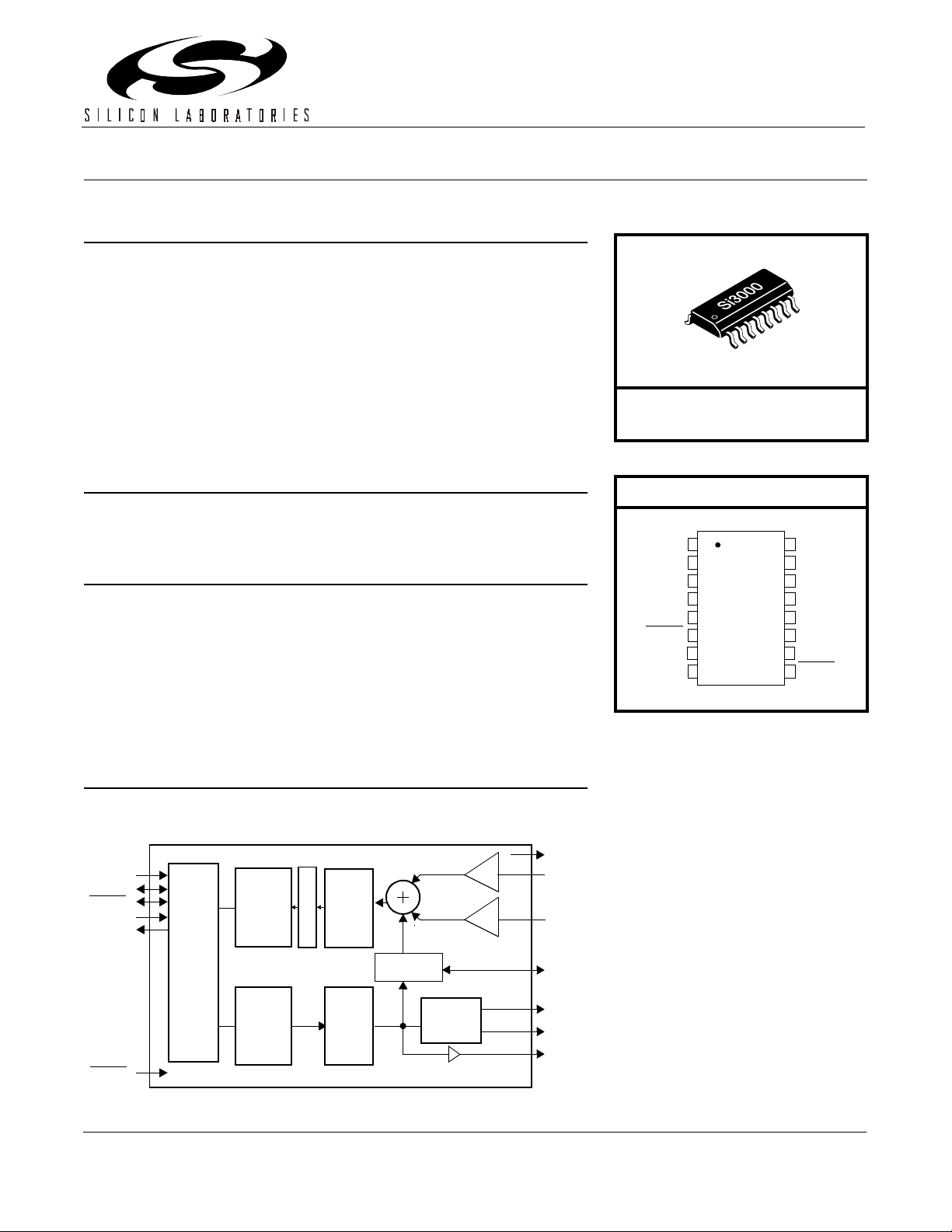
Si3000
R
V
OICEBAND
C
ODEC WITH
M
ICROPHONE
Features
Complete voice codec solution includes the following:
!
84 dB ADC Dynamic Range
!
84 dB DAC Dynamic Range
!
4–12 kHz Sample Rates
!
30 dB Microphone Pre-Amp
!
Programmable Input Gain/
Attenuation: –36 dB to 12 dB
!
Programmable Output Gain/
!
Support for 32 Ω Headphones
!
3:1 Analog Input Mixer
!
3.3–5.0 V Power Supply
!
Direct Interface to DSPs
!
Direct Connection to Si3034,
Si3035, and Si3044 ISOcap
!
Low profile 16 Pin SOIC Package
™
DAA
Attenuation: –36 dB to 12 dB
Applications
!
Modem Voice Channel (DSVD)
!
Telephony
!
Speech Processing
!
General Purpose Analog I/O
Description
The Si3000 is a complete voice band audio codec solution that offers high
integration by incorporating programmable input and output gain/
attenuation, a microphone bias circuit, handset hybrid circuit, and an
output drive for 32 Ω headphones. The Si3000 c an be connec ted di rectly
to the Si3034, Si3035, and Si3044 ISOcap North American and
international DAA chipsets through its daisy-chaining serial interface. The
device operates from a singl e 3.3 to 5 V power supply and is avail able in
a 16-pin small outline package (SOIC).
/S
PEAKER
Ordering Information:
See page 30.
Pin Assignments
Si3000
SPKRR
MBIAS
HDST
FSYNC
MCLK
SCLK
SDI
SDO
1
2
3
4
5
6
7
8
D
16
15
14
13
12
11
10
9
RIVE
SPKRL
LINEO
GND
V
A
V
D
LINEI
MIC
RESET
Functional Block Diagram
Si3000
0/+10/+20/+30 dB
MCLK
SCLK
FSYNC
SDI
SDO
RESET
Digital
Interface
Prog Gain/
Attenuator
Prog Gain/
Attenuator
High Pass Filter
ADC
0/+10/+20 dB
Handset
Hybrid
0/–6/–12/–18 dB
Headphone
DriverDAC
0/–6/–12/–18 dB
Rev. 1.1 6/00 Copyright © 2000 by Silicon Laboratories Si3000-DS11
MBIAS
MIC
LINEI
HDST
SPKR
SPKRL
LINEO
Page 2

Si3000
2 Rev. 1.1
Page 3

Si3000
T
ABLE OF
C
ONTENTS
Section Page
Electrical Specifications . . . . . . . . . . . . . . . . . . . . . . . . . . . . . . . . . . . . . . . . . . . . . . . . . 4
Functional Description . . . . . . . . . . . . . . . . . . . . . . . . . . . . . . . . . . . . . . . . . . . . . . . . . . 14
Analog Inputs . . . . . . . . . . . . . . . . . . . . . . . . . . . . . . . . . . . . . . . . . . . . . . . . . . . . . . . 14
Pre-amp/Microphone Bias Circuit . . . . . . . . . . . . . . . . . . . . . . . . . . . . . . . . . . . . . . . 14
Programmable Input Gain/Attenuation . . . . . . . . . . . . . . . . . . . . . . . . . . . . . . . . . . . . 14
Analog Outputs . . . . . . . . . . . . . . . . . . . . . . . . . . . . . . . . . . . . . . . . . . . . . . . . . . . . . 14
Programmable Output Gain/Attenuation . . . . . . . . . . . . . . . . . . . . . . . . . . . . . . . . . . 15
Line Output . . . . . . . . . . . . . . . . . . . . . . . . . . . . . . . . . . . . . . . . . . . . . . . . . . . . . . . . . 15
Speaker Output . . . . . . . . . . . . . . . . . . . . . . . . . . . . . . . . . . . . . . . . . . . . . . . . . . . . . 15
Digital Interface . . . . . . . . . . . . . . . . . . . . . . . . . . . . . . . . . . . . . . . . . . . . . . . . . . . . . 15
Clock Generation Subsystem . . . . . . . . . . . . . . . . . . . . . . . . . . . . . . . . . . . . . . . . . . . 17
Sleep Mode . . . . . . . . . . . . . . . . . . . . . . . . . . . . . . . . . . . . . . . . . . . . . . . . . . . . . . . . 18
Loopback Operation . . . . . . . . . . . . . . . . . . . . . . . . . . . . . . . . . . . . . . . . . . . . . . . . . . 19
Reducing Power-on Pop Noise . . . . . . . . . . . . . . . . . . . . . . . . . . . . . . . . . . . . . . . . . 19
Control Registers . . . . . . . . . . . . . . . . . . . . . . . . . . . . . . . . . . . . . . . . . . . . . . . . . . . . . . . 20
Ordering Guide . . . . . . . . . . . . . . . . . . . . . . . . . . . . . . . . . . . . . . . . . . . . . . . . . . . . . . . . . 30
Package Outline . . . . . . . . . . . . . . . . . . . . . . . . . . . . . . . . . . . . . . . . . . . . . . . . . . . . . . . . 31
Contact Information . . . . . . . . . . . . . . . . . . . . . . . . . . . . . . . . . . . . . . . . . . . . . . . . . . . . . 36
Rev. 1.1 3
Page 4
Si3000
Electrical Specifications
Table 1. Recommended Operating Conditions
Parameter Symbol Test Condition
Ambient Temperature T
Si3000 Supply Voltage, Analog
Si3000 Supply Voltage, Digital
2
2,3
A
V
A
V
D
K-grade 0 25 70 °C
1
Min
Typ
3.0 3.3/5.0 5.25 V
3.0 3.3/5.0 5.25 V
Max
1
Unit
Notes:
1. All minimum and maximum specifications are guaranteed and apply across the recommended operating conditions.
Typical values apply at nominal supply voltages and an operating temperature of 25°C unless otherwise stated.
2. The digital supply, V
3.3 V logic when operating from 3.3 V. V
3.
The Si3000 specifications are guaranteed using the typical application circuit (including component tolerance) of
and analog supply, VA, can operate from either 3.3 V or 5.0 V. The Si3000 supports interface to
D,
must be within 0.6 V of VA.
D
Figure 13.
Table 2. DC Characteristics, VA/VD = 5 V
(VA = 5 V ±5%, VD = 5 V ±5%, TA = 0 to 70°C for K-grade)
Parameter Symbol Test Condition Min Typ Max Unit
High Level Input Voltage V
Low Level Input Voltage V
High Level Output Voltage V
Low Level Output Voltage V
Input Leakage Current I
Power Supply Current, Analog
Power Supply Current, Digital
Total Supply Current, Sleep Mode
1
2
3
I
I
IH
IL
OH
OL
L
A
D
IO = –2 mA 3.5 — — V
IO = 2 mA — — 0.4 V
VA pin — 6.5 10 mA
VD pin — 10 15 mA
Notes:
1. No loads at D AC outputs, no load at MBIAS, Fs=12.5 kHz.
2.
Slave mode operation, Fs = 12.5 kHz.
3. All inputs, except MCLK, are held static, and all outputs are unloaded.
3.5 — — V
——0.8V
–10 — 10 µA
——1.5mA
Table 3. DC Characteristics, VA/VD = 3.3 V
(VA = 3.3 V ±10%, VD = 3.3 V ±10%, TA = 0°C to 70°C for K-grade)
Parameter Symbol Test Condition Min Typ Max Unit
High Level Input Voltage V
Low Level Input Voltage V
High Level Output Voltage V
Low Level Output Voltage V
Input Leakage Current I
Power Supply Current, Analog I
Power Supply Current, Digital
Total Supply Current, Sleep Mode
2
3
I
IH
IL
OH
OL
L
A
D
IO = –2 mA 2.4 — — V
IO = 2 mA — — 0.35 V
VA pin — 6 10 mA
VD pin — 6 10 mA
Notes:
1. No loads at D AC outputs, no load at MBIAS, Fs=12.5 kHz.
2. Slave mode operation, Fs = 12.5 kHz.
3. All inputs, except MCLK, are held static, and all outputs are unloaded.
4 Rev. 1.1
2.4 — — V
——0.8V
–10 — 10 µA
——1.5mA
Page 5
Si3000
Table 4. AC Characteristics
(VA, VD = 5 V ±5% or 3.3 V ±10%, TA = 0°C to 70°C for K-grade)
Parameter Symbol Test Condition Min Typ Max Unit
ADC Resolution —16—Bits
ADC Dynamic Range
ADC Total Harmonic Distortion
1,2
3
VA, VD = 3.3 V ±10% VIN = 1 kHz, –3 dB, HDST — –80 –62
ADC Total Harmonic Distortion
3
VA, VD = 5 V ±5% VIN = 1 kHz, –3 dB, HDST — –80 –71
ADC Full Scale Level (0 dB gain)
ADC Programmable Input Gain –36 — 12 dB
ADC Input Gain Step Size — 1.5 — dB
ADC Freq Response
ADC Freq Response
5
5
ADC Freq Response F
Line In Preamp Gain — 0/10/20 — dB
ADCDR VIN = 1 kHz , –3 dB 80 84 — dB
ADCTHD VIN = 1 kHz, –3 dB, MIC/LINEI — –80 –62 dB
ADCTHD VIN = 1 kHz, –3 dB, MIC/LINEI — –80 –76 dB
4
V
RX
F
RR
F
RR
RR
Vin = 1 kHz — 1 — V
Low –3 dB corner — 33 — Hz
300 Hz –0.1 — 0 dB
3400 Hz –0.2 — 0 dB
rms
Mic In Preamp Gain — 0/10/20/
—dB
30
ADC Input Resistance 0 dB Preamp Gain — 20 — kΩ
ADC Input Capacitance — 15 — pF
ADC Gain Drift A
T
VIN = 1 kHz — 0.002 — dB/°C
DAC Resolution —16—Bits
DAC Dynamic Range
DAC Total Harmonic Distortion
VA, VD = 3.3 V ±10% VIN=1 kHz,–6 dB, SPKR, 60
DAC Total Harmonic Distortion
1,2
DACDR VIN = 1 kHz, –6 dB 80 84 — dB
3
3
DACTHD VIN=1 kHz,–6 dB,LINEO,600 Ω — –76 –60 dB
Ω
— –72 –60
VIN=1 kHz,–6 dB, HDST, 600
Ω
— –80 –70
DACTHD VIN=1 kHz,–3 dB,LINEO,600 Ω — –76 –65 dB
VA, VD = 5 V ±5% VIN=1 kHz,–3 dB, SPKR, 60 Ω — –72 –65
VIN=1 kHz,–3 dB, HDST, 600 Ω — –80 –76
DAC Full Scale Level (0 dB gain) V
RX
—1—V
rms
DAC Programmable Output Gain –36 — 12 dB
Notes:
1. DR = VIN + 20 log (RMS signal/RMS noise). Measurement bandwidth is 300 to 3400 Hz. Valid sample rate ranges
between 4000 and 12000 Hz.
2. 0 dB setting for analog and digital attenuation/gain.
3. THD = 20 log (RMS distortion/RMS signal). Valid sample rate ranges between 4000 and 12000 Hz.
4. At 0dB gain setting, 1 V
input corresponds to -1.5 dB of full scale digital output code.
rms
5. These characteristics are determined by external components. See Figure13.
6. With a 600 Ω load. Output starts clipping with half of full scale digital input, which corresponds to a 0.5 V
rms
output.
Rev. 1.1 5
Page 6
Si3000
Table 4. AC Characteristics (Continued)
(VA, VD = 5 V ±5% or 3.3 V ±10%, TA = 0°C to 70°C for K-grade)
Parameter Symbol Test Condition Min Typ Max Unit
DAC Output Gain Step Size — 1.5 — dB
DAC Freq Response
DAC Freq Response
DAC Freq Response F
DAC Line Output Load Resistance 600 — — Ω
DAC Line Output Load Capacitance — — 40 pF
DAC SPKR Output Load Resistance — 60 — Ω
5
5
F
RR
F
RR
RR
Low –3 dB corner — 33 — Hz
300 Hz –0.01 — 0 dB
3400 Hz –0.2 — 0 dB
DAC Gain Drift A
T
VIN = 1 kHz — 0.002 — dB/°C
Interchannel Isolation (Crosstalk) — 90 — dB
HDST Full Scale Level Input — 0.5 — V
HDST Full Scale Level Output
6
—1.0—V
HDST Output Resistance Rout DC — 600 —
MIC Bias Voltage V
mbias
—2.5—V
MIC Power Supply Rejection Ratio PSRR — 40 — dB
Notes:
1.
DR = VIN + 20 log (RMS signal/RMS noise). Measurement bandwidth is 300 to 3400 Hz. Valid sample rate ranges
between 4000 and 12000 Hz.
2.
0 dB setting for analog and digital attenuation/gain.
3. THD = 20 log (RMS distortion/RMS signal). Valid sample rate ranges between 4000 and 12000 Hz.
4. At 0dB gain setting, 1 V
input corresponds to -1.5 dB of full scale digital output code.
rms
5. These characteristics are determined by external components. See Figure 13.
6.
With a 600 Ω load. Output starts clipping with half of full scale digital input, which corresponds to a 0.5 V
rms
output.
Table 5. Absolute Maximum Ratings
Parameter Symbol Value Unit
DC Supply Voltage V
Input Current, Si3000 Digital Input Pins I
Digital Input Voltage V
Operating Temperature Range T
Storage Temperature Range T
D
IND
STG
, V
IN
A
A
Note: Permanent device damage may occur if the above Absolute Maximum Ratings are exceeded. Functional operation
should be restricted to the conditions as specified in the operational sections of this data sheet. Exposure to absolute
maximum rating conditions for extended periods may affect device reliability.
–0.5 to 6.0 V
±10 mA
–0.3 to (VD + 0.3) V
–10 to 100 °C
–40 to 150 °C
rms
rms
Ω
6 Rev. 1.1
Page 7
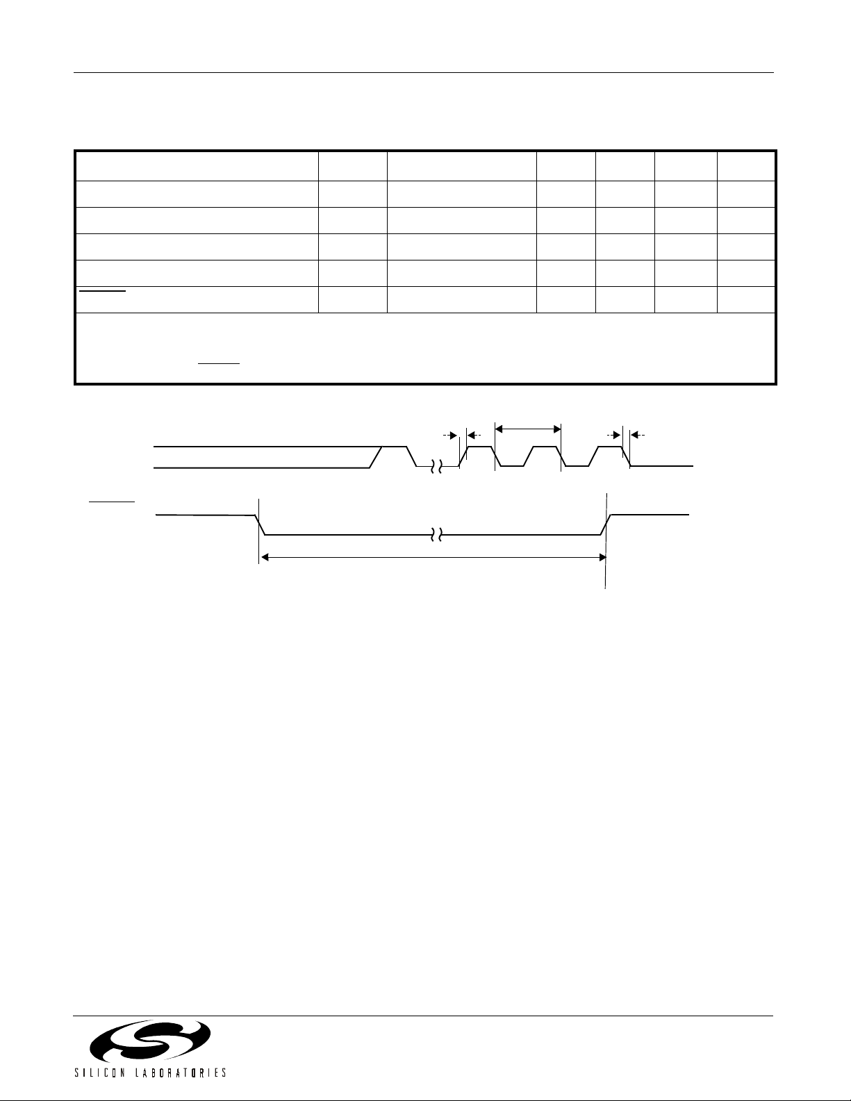
Table 6. Switching Characteristics—General Inputs
(VA, VD = 5 V ±5% or 3.3 V ±10%, TA = 70°C for K-grade, CL = 20 pF)
Si3000
Parameter
1
Cycle Time, MCLK t
MCLK Duty Cycle t
Rise Time, MCLK t
Fall Time, MCLK t
RESET
Notes:
Pulse Width
1. All timing (except Rise and Fall time) is referenced to the 50% level of the waveform. Input test levels are V
0.4 V, V
2.
The minimum RESET
2
= 0.4 V. Rise and Fall times are referenced to the 20% and 80% levels of the waveform.
IL
pulse width is the greater of 5 µs or 10 MCLK cycle times.
Symbol Test Condition Min Typ Max Unit
mc
dty
t
r
f
rl
t
r
16.67 — — ns
40 50 60 %
—— 5 ns
—— 5 ns
250 — — ns
t
mc
t
f
MCLK
RESET
IH
V
IH
V
IL
= VD –
t
rl
Figure 1. General Inputs Timing Diagram
Rev. 1.1 7
Page 8
Si3000
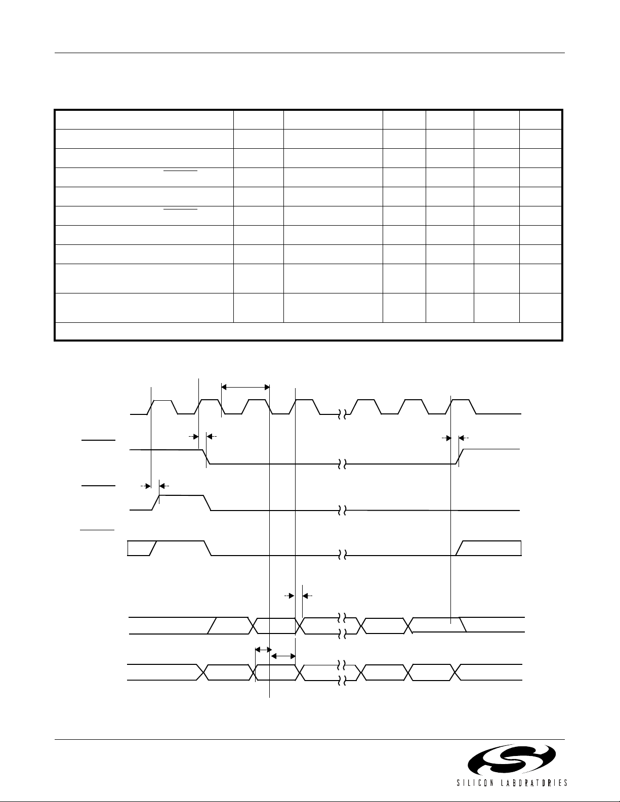
Table 7. Switching Characteristics—Serial Interface
(VA, VD = 5 V ±5% or 3.3 V ±10%, TA = 70°C for K-grade, CL = 20 pF)
Parameter Symbol Test Condition Min Typ Max Unit
Cycle Time, SCLK t
SCLK Duty Cycle t
Delay Time, SCLK ↑ to FSYNC
↓ t
Delay Time, SCLK ↑ to SDO Valid t
Delay Time, SCLK ↑ to FSYNC
↑ t
Setup Time, SDI, before SCLK ↓ t
Hold Time, SDI, after SCLK ↓ t
Setup Time, FSYNC (mode 2) before
c
dty
d1
d2
d3
su
h
t
su
354 1/256 Fs — ns
25 — — ns
20 — — ns
25 — — ns
MCLK ↓
Hold Time, FSYNC (mode 2) after
t
h
20 — — ns
MCLK ↓
Note: All timing is referenced to the 50% level of the waveform. Input test levels are V
t
c
SCLK
t
d1
FSYNC
(mode 0)
—50—%
— — 10 ns
— — 20 ns
— — 10 ns
= VD – 0.4 V, VIL = 0.4 V
IH
V
OH
V
OL
t
d3
t
FSYNC
(mode 1)
d3
FSYNC
(mode 2)
t
16-bit
SDO
16-bit
SDI
High-Z
D15
D15
D14
t
su
D14
... D2
t
h
... D2
Figure 2. Serial Interface Timing Diagram
8 Rev. 1.1
d2
D1
D1
D0
D0
High-Z
Page 9
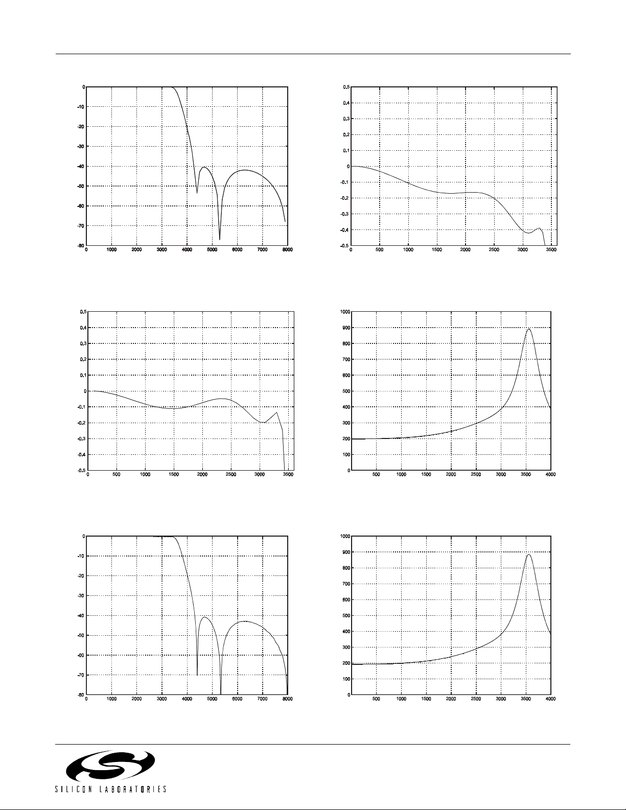
Table 8. Digital FIR Filter Characteristics—Transmit and Receive
(VA, VD = 5 V ±5% or 3.3 V ±10%, Sample Rate = 8 kHz, TA = 70°C for K-Grade)
Parameter Symbol Min Typ Max Unit
Si3000
Passband (3 dB, HPFD = 1)
Passband (3 dB, HPFD = 0)
F
(3 dB)
F
(3 dB)
Passband Ripple Peak-to-Peak
Stopband
Stopband Attenuation
Group Delay
Note:
Typical FIR filter characteristics for Fs = 8000 Hz are shown in Figures 3, 4, 5, and 6.
t
gd
0—3.6kHz
0.01 — 3.6 kHz
–0.1 — 0.1 dB
—4.4—kHz
–74 — — dB
— 12/Fs — sec
Table 9. Digital IIR Filter Characteristics—Transmit and Receive
(VA, VD = 5 V ±5% or 3.3 V ±10%, Sample Rate = 8 kHz, TA = 70°C for K-Grade)
Parameter Symbol Min Typ Max Unit
Passband (3 dB, HPFD = 1)
Passband (3 dB, HPFD = 0)
F
(3 dB)
F
(3 dB)
Passband Ripple Peak-to-Peak
Stopband
Stopband Attenuation
Group Delay
Note: Typical IIR filter characteristics for Fs = 8000 Hz are shown in Figures 7, 8, 9, and 10. Figures 11 and 12 show group
delay versus input frequency.
t
gd
0—3.6kHz
0.01 — 3.6 kHz
–0.2 — 0.2 dB
—4.4—kHz
–40 — — dB
— 1.6/Fs — sec
Rev. 1.1 9
Page 10

Si3000
Attenuation - dB
Input Frequency - Hz
Figure 3. FIR Receive Filter Response
Attenuation - dB
Input Frequency - Hz
Figure 4. FIR Receive Filter Passband Ripple
Attenuation - dB
Input Frequency - Hz
Figure 5. FIR Transmit Filter Response
Attenuation - dB
Input Frequency - Hz
Figure 6. FIR T ransmi t Filter Passband Ripple
For Figures 3–6, all filter plots apply to a sample rate of
Fs = 8 kHz. The filters scale with the sample rate as follows:
F
where Fs is the sample frequency.
10 Rev. 1.1
(0.1 dB)
F
(– 3 dB)
= 0.4125 Fs
= 0.45 Fs
Page 11
Si3000
Attenuation - dB
Input Frequency - Hz
Figure 7. IIR Receive Filter Response
Attenuation - dB
Input Frequency - Hz
Figure 8. IIR Receive Filter Passband Ripple
Attenuation - dB
Input Frequency - Hz
Figure 10. IIR Transmit Filter Passband Ripple
Delay - µs
Input Frequency - Hz
Figure 11. IIR Receive Group Delay
Attenuation - dB
Input Frequency - Hz
Figure 9. IIR T ransmit Filter Response
Delay - µs
Input Frequency - Hz
Figure 12. IIR Transmit Group Delay
Rev. 1.1 11
Page 12

12 Rev. 1.1
Si3000
Figure 13. Si3000 Typical Application Circuit
Page 13

Si3000
‘
Table 10. Component Values—Typical Application
Symbol Value
C1,C3,C6,C8 0.1 µF, 16 V, ±20%
C2,C4,C5,C7,C9,C10 10 µF, 16 V, ±20%
D1 Motorola MMBD914L
J1,J2 Phonejack Stereo
JP1 4 Header
K1 Relay DPDT
L1,L2 Ferrite Bead
R1 0 Ω, 1/4 W
R2 51 Ω, 1/4 W
R4 10 kΩ, 1/4 W
R8 2.2 k, 1/4 W, ±5%
R9 10 Ω, 1/16 W, ±5%
R11,R12 30 Ω, 1/16 W, ±5%
U2 LM317LZ
±
5%
±
±
5%
5%
Q1 PNP Transistor
Rev. 1.1 13
Page 14

Si3000
Functional Description
The Si3000 is a highly integrated voice bandwidth audio
codec which contains a singl e 16-bit A/D converte r and
D/A converter. The analog input path contains a
microphone input w ith selec table gai n, a line l evel inpu t
with selectable gai n, and a handset input. Each o f the
inputs go through a mixer prior to A/D conv ersion. The
result of this A/D con version is a 16-bit si gned number.
Following the A/D con verter is a digital programmable
gain amplifier. The analog output path contains a digital
programmable gain amplifier feeding a single 16-bit D/A
converter. The DAC output is provided to a line output, a
headphone drive outp ut, and a hands et output. Control
for the various function s av ailable on the Si3000 as well
as the audio data ar e commu nicated to the devi ce over
a serial interface.
The Si3000 can be connected directly to the Si3035,
Si3034, Si3044 in modem ap pli cati ons re quiri ng a voic e
channel, or the device can be used as a stand-alone
codec in other voice band applications. The Si3000
offers high integration, and it need s onl y a few low cost,
discrete components as shown in Figure 13.
Analog Inputs
The typical connection diagram (Figure 13) shows the
recommended exte rnal analog circuitry for th e Si3000.
The device supports three mono analog inputs—line
level, microphone level, and a handset input. Each of
these inputs is provided to a mixer circuit prior to A/D
conversion. Each analog input may also be muted by
writing the appropriate bits in the control registers.
Unused analog inpu ts shou ld be tied to GND t hrough a
0.1 µF capacitor. This prevents any DC current flow.
Pre-amp/Microphone Bias Circuit
An internal amplifier with a selectable gain of 0 dB,
10 dB, 20 dB, or 30 dB is provided for the MIC input and
an internal amplifier with a selectable gain of 0 dB,
10 dB, or 20 dB, is provided for the LINEI input. AC
coupling is required for both inputs because any DC
offset on the input will be ampl ified if gain is selected.
Gain settings for the LINEI and MIC inputs are achieved
by writing the RX Gain Control 1 r egister 5. When gain
is disabled, these input s becom e line l evel in put s with a
full scale input of 1 Vrms.
A microphone bias circuit is provided on-chip which
consists of a 2.5 V reference output capable of sourcing
up to 5 mA of current. This circuit can be used for active
microphones requiring a bias source.
Programmable Input Gain/Attenuation
The signals from the microphone, line, or handset
inputs are mixed and then routed to the A/D conv erter
and a digital prog rammable gain circ uit which provides
up to 12 dB of gain or –34.5 dB of attenuati on in 1.5 dB
steps. Level chan ges only take e ffect on zer o cros sings
to minimize audible artifacts. The requested level
change is implemented if no zero crossing is found after
256 frames. Write the ADC Volume Control register 6 to
set digital input gain/attenuation.
Analog Outputs
The analog outpu ts of the D/A conve rter a re routed to a
line level output (LINEO), a pair of speaker outputs
(SPKRL and SPKRR), and a handset. Each analog
output can be independently muted.
Si3034/35/44 Chipsets
Si3021 DAA
(Master)
DSP
Si3000
Voice Codec
Figure 14. Si3000 with Silicon Labs DAA System Diagram
14 Rev. 1.1
Si3012 DAA
or
Si3014 DAA
or
Si3015 DAA
SPKR
Line
Discretes
Handset
Mic
TIP
RING
Page 15

Si3000
Programmable Output Gain/Attenuation
Prior to D/A conversion, the Si3000 contains a digital
programmable gain/attenuator which provi des up to 12 dB
of gain or –34.5 dB of attenuation in 1.5 dB steps. Level
changes only take effect on zero crossings to minimize
audible artifacts. The requested level change is
implemented if no zero crossing is found after 256 frames.
Write the DAC Volume Control (register 7) to set digital
input gain/attenuation.
Line Output
LINEO is a line l evel analog output signal centered around
a common mode voltage. The minimum recommended
load impedance is 600
output with a 1 Vrms full scale range. The only external
component required is the 10
shown in Figure 13 on page 12. This output may be muted
through the LOM bit in register 6 or attenuated by setti ng
the analog attenuation bits in register 9.
Ω
. This output is a fully filtered
µ
F DC blocking capacitor
Speaker Output
The SPKRL and SPKRR analog outputs are capable of
driving a small loudspeaker whose impedance is typical ly
32
Ω
(see Figure 13 on page 12). The speaker outputs
may be muted through the SLM and SRM bits in the DAC
Gain Control register 7 or att enuated by set t ing t he anal og
attenuation bits in register 9.
Digital Interface
The Si3000 has two serial interface modes that support
most standard modem DSPs. These modes are selected
by the addition of a 50 k
SDO and SCLK pins as shown in Figure 13 on page 12. To
determine the mode, the Si3000 reads SDO and SCLK on
the first ris ing edge of MCLK after RESET
key difference between these two serial modes is the
operation of the FSYNC
serial mode definitions.
Table 11. Serial Modes
Mode SCLK* SDO* Description
000FSYNC
101FSYNC
2 1 0 Slave mode
3 1 1 Reserved
*Note: Pull-up/pull-down states
The digital interface consists of a single synchronous serial
link which communicates audio and control data.
In slave mode, SCLK is connected only to the pullup/
Ω
pull-down/up resistor on the
goes low. The
signal. Table 11 summarizes the
frames data
pulse start s data
frame
pulldown resistor, and MCLK is a 256 Fs input which is
internally multiplied using the on-chip phase-locked loop
(PLL) to clock the A/D converter and D/A converter. In
master mode, the master clock (MCLK) is an input and the
serial data clock (SCLK) is an output. The MCLK frequency
and the value of the sample rate cont rol regist ers 3 and 4
determine the sample rate (Fs). The serial port clock,
SCLK, runs at 256 bits per frame, where the frame rate is
equivalent to the sample rate.
Digital informati on is t ransf er red bet ween the DSP and the
Si3000 in the form of 16-bit Primary Frames and 16-bit
Secondary Frames. There are separate pins for receive
(SDO) and transmit (SDI) functions, providing
simultaneous receive/transmit operation within each frame.
Primary Frames are used for digit al audio data samples.
Primary Frames occur at the frame rate and are always
present.
Secondary Frames are used for accessing internal Si 3000
registers. Secondary Frames ar e not always present and
are requested on-demand. When Secondary Frames are
present, they occur mid-point between Primary Frames.
Hence, no Primary Frames are dropped.
On Primary Frame transmits (DSP to Si3000), the Si3000
treats the LSB (16th bit) as a fl ag to request a Secondary
Frame. Therefore, out of 16-bits of transmit dat a on SDI,
only 15-bits represent actual audio data. When secondary
frames are not present, no t ransmissi on oc cur s during t his
time slot.
On Primary Frames receives (Si3000 to DSP), t he Si3000
drives SDO with 16-bits of audio data, if the Si3000 is i n
either Serial Mode 0 or 1. However, if the Si3000 is in
SLAVE mode (Mode 2), the Si3000 supplies 15-bits of
Audio Data to the DSP and always drives the LSB zero.
This feature is designed to work with the Si3021 register 14
SSEL set to 10. In this system configuration, when the
DSP receives Primary Frames, it can check the LSB to
determine whether the receive data is fr om the Si3021 or
from the Si3000.
On Secondary Frame receives and transmits; the Si3000
treats the input and output serial stream as 16-bits of data.
Figure 15 shows the relative timing of the serial frames.
Figure 16 and Figure 17 illustrate the secondary frame
write cycle and read cycle, respectively. During a read
cycle, the R/W
contains the address of the register to be read. The
contents of the 8-bit control register are placed on the SDO
signal. During a write cycle, the R/W
address field contains the address of the register to be
written. The 8-bit data to be written immediately follows the
address on SDI. Only one register can be read or written
during each secondary frame. See "Control Regi sters‚ " on
page 20 for the register addresses and functions.
bit is high and the 5-bit address field
bit is low and the 5-bit
Rev. 1.1 15
Page 16

Si3000
FSYNC
SDI
SDO
Primary
D15-D1 D0=1 (Software FC Bit)
XMT Data
RCV Data
16 SCLKS
128 SCLKs
Secondary
Secondary
Update
Secondary
Update
256 SCLKs
Figure 15. Secondary Request
Primary
XMT Data
RCV Data
FSYNC
(mode 0)
FSYNC
(mode 1)
SDI
D15 D14 D13 D12 D11 D10 D9 D8
AA AA A
000
D7 D6 D5 D4 D3 D2 D1 D0
DDD DDDD D
R/W
SDO
High Z
Figure 16. Secondary Communication Data Format—Write Cycle
High Z
16 Rev. 1.1
Page 17

FSYNC
(mode 0)
FSYNC
(mode 1)
Si3000
SDI
SDO
MCLK
D15 D14 D13 D12 D11 D10 D9 D8
AA AA A
100
High Z High Z
R/W
D7
D7 D6 D5 D4 D3 D2 D1 D0
DDDDD
D
D0
D
D
Figure 17. Secondary Frame Format—Read Cycle
F
÷
N1
8 bits
UP1
P
D
÷
M1
8 bits
VCO1
F
PLL1
÷
5 or
÷
10 *
*Note:
1024 • fs
See PLL bit in Register 2
Figure 18. Clock Generation Subsystem (PLL)
Clock Generation Subsystem
The Si3000 contai ns an on-chip cl ock generator. Using
a single MCLK input frequency, the Si3000 can
generate all the desi red stand ard m odem samp le ra tes,
as well as the common 11.025 kHz rate for audio
playback.
The clock generator consists of a phase-locked loop
(PLL1) that achieves the desired sample frequency.
Figure 18 illustrates the clock generator. The
architecture of the PLL all ows for f ast lock ti me on init ial
start-up, fast lock time when changing modem s ample
rates and high noise immunity. A large number of MCLK
frequencies between 1 MHz and 60 MHz are supported.
Programming the Clock Generator
As noted in Figure 18, the clock generator must output a
clock equal to 102 4*Fs , wher e Fs i s th e des ired s am pl e
Rev. 1.1 17
rate. The 1024*Fs clock is determined through
programming of the following registers:
Register 3 - N1 divider, 8 bits.
Register 4 - M1 divider, 8 bits
N1 (register 3) and M1 (register 4) are 8-bit unsigned
values. F
is the clock provided to the MCLK pin.
MCLK
Table 12 list several s tand ar d cr y st al r ate s tha t could be
supplied to MCLK.
When programming the registers of the clock generator,
the order of register writes is important. For PLL
updates, N1 (register 3) must always be written first,
immediately followed by a write to M1 (register 4).
Note: The values shown in Table 12 satisfy the equations
above. However, when programming the registers for
N1 and M1, the value pla ced in these re gisters must be
one less than the value calculated from the equations.
Page 18

Si3000
Table 12. MCLK Examples for 8 kHz
MCLK (MHz) N1 M1
1.8432 9 200
4.0000 25 256
4.0960 1 10
5.2800 33 256
5.7600 9 64
6.1440 3 20
8.1920 1 5
9.2160 9 40
10.0800 63 256
10.5600 33 128
11.0592 27 100
12.288 3 10
14.7456 9 25
16.0000 25 64
18.4320 9 20
24.5760 3 5
25.8048 63 100
33.7600 211 256
44.2368 27 25
46.0800 9 8
47.9232 117 100
48.0000 75 64
56.0000 175 128
59.200 185 128
PLL Lock Times
The Si3000 changes sample rates very quickly.
However, lock time will vary based on the programming
of the clock generator. The following relationship
describes the boundaries on PLL locking time:
PLL lock time < 1 ms
It is recommended tha t the PLL be prog rammed durin g
initialization.
The final design consid eration fo r the cloc k genera tor is
the update rate of P LL. The following criteria must be
satisfied in order for the PLL to remain stable:
Where F
F
UP1FMCLK
is shown in Figure 18.
UP1
N1()⁄= 144kHz≥
Setting Generic Sample Rates
The above clock generation description focuses on
common modem sample rates. The restrictions and
equations above still apply; however, a more generic
relationship between MCLK and Fs (the desired sam ple
rate) is needed. The following equation describes this
relationship:
M1
------- -
N1
⋅⋅
51024Fs
--------------------------------=
MCLK
where Fs is the sample frequency, and all other symbols
are shown in Figure 18.
Knowing the MCLK frequency and desired sample rate
the values for the M1 and N1 registers can be
determined. When determining these values, remember
to consider the range f or each register as well as the
minimum update rate for the first PLL.
The values determined for M1 and N1 must be adjusted
by minus one when dete rmin ing the va lu e written to the
respective registers. Th is is due to internal logic, which
adds one to the value stored in the register. This
addition allows t he user to write a zero value in any of
the registers and the effective divide-by is one. A
special case occurs when both M1 and N1 are
programmed with a zero val ue. When M1 and N1 are
both zero, the PLL is bypassed.
Sleep Mode
The Si3000 supports a low-power sleep mode. Sleep
mode is activated by setting the Chip Power Down
(CPD) bit in register 1. When the Si3000 is in sleep
mode, the MCLK signal may be stopped or remain
active, but it must be active before waking up the
Si3000. To take the Si3000 out of sleep mode, pulse the
reset pin (RESET
sequence is as follows:
1. Set the Power Down bit (PDN, re gister 6, bit 3).
2. MCLK may stay active or stop.
3. Restore MCLK before initiating the power up sequence.
4. Reset the Si3000 using the RESET
present).
5. Program the registers to desired settings.
) low. In summary, the pow er down/u p
pin (after MCLK is
18 Rev. 1.1
Page 19

Loopback Operation
The Si3000 advanced design provides the
manufacturer with increased ability to determine system
functionality during production line tests, as well as
support for end-user diagnostics. Two loopback modes
exist for this purpose, allowing increased coverage of
system components.
The digital loopback1 mode allows an external device to
send audio data to the SDI input pin and receive the
signal through the SDO output pin. In this mode, the
group delay of the digital filters is present. This mode
allows testing of the digital filters, DAC, and ADC. To
enable this mode, set the DL bit of register 2.
The digital loopback2 mode allows an external device to
send audio data to the SDI input pin and receive the
signal through the SDO output pin. This mode allows
testing of the digital filters, but not the ADC and DAC.
Reducing Power-on Pop Noise
To minimize power-on pop during initialization, a waiting
period is recommended befor e powering up the analog
output drivers. The waitin g period starts when the reset
signal to the Si3 000 is negated. The wait time r equired
is dependent on the external load. Typically, the load
consists of an AC coupling capacitor in s eries with an
equivalent load resist or to ground. The equivalent load
resistor can either be a speaker load, or the input
resistance of an external amplifier. The rule-of-thumb for
the waiting period in msec is der ived by C*(12+R). For
example, in the case of a 10 µF AC coupling capacitor
and resistive load of 1.0 kΩ the r ecommended waiting
period is 10*(12+1) = 130 msec.
If the analog outputs dri ve external amplifiers, another
factor to consider is the voltage division ratio
determined by R/(R+1 2), where R represents the i nput
resistance of the external am plifier. This ratio must be
kept as small as possible. A go od target value is R = 1
kΩ. If needed, add a load resistor in parallel with the
amplifier input to lower th e effective input resistance of
the amplifier stage.
Si3000
Rev. 1.1 19
Page 20

Si3000
Control Registers
Note: Any register not listed here is reserved and should not be written. Any register bit labelled reserved should be written to
zero during writes to the register. Register 0 can be read (always returns 0) and written safely.
T able 13. Register Summary
Register Name Bit 7 Bit 6 Bit 5 Bit 4 Bit 3 Bit 2 Bit 1 Bit 0
1 Control 1 SR SPD LPD HPD MPD CPD
2 Control 2 HPFD PLL DL1 DL2
3 PLL1 Divide N1 Divider N1
4 PLL1 Multiply M1 Multiplier M1
5 RX Gain Control 1 LIG LIM MCG MCM HIM IIR
6 ADC Volume Control RXG LOM HOM
7 DAC Volume Control TXG SLM SRM
8 Status Report SLSC SRSC LOSC
9 Analog Attenuation LOT SOT
20 Rev. 1.1
Page 21

Register 1. Control 1
Bit D7D6D5D4D3D2D1D0
Name SR SPD LPD HPD MPD CPD
Type R/W R/W R/W R/W R/W R/W
Reset settings = 0000_0000
Bit N ame Function
7SRSoftware Reset.
1 = Sets all registers to their reset value.
0 = Enables chip for normal operation.
Note: Bit will automatically clear after being set.
6:5 Reserved Read returns zero.
4SPDSpeaker Drive Power Down.
1= Normal operation
0 = Power down left and right speaker drive.
3LPDLine Drive Power Down.
1 = Normal operation
0 = Power down line driver.
2HPDHandset Drive Power Down.
1 = Normal operation
0 = Power down handset driver.
1MPDMIC Bias Power Down.
1 = Power down MIC bias buffer.
0 = Normal operation
0CPDChip Power Down.
1 = Puts Si3000 into power down mode.
0 = Normal operation
Si3000
Rev. 1.1 21
Page 22

Si3000
Register 2. Control 2
BitD7D6D5 D4 D3D2D1D0
Name HPFD PLL DL1 DL2
Type R/W R/W R/W R/W
Reset Set
tings = 0000_0000
Bit Name Function
7:5 Reserved Read returns zero.
4HPFDHigh Pass Filter (HPF) Disable.
1 = HPF disabled
0 = HPF enabled
3PLLPLL Divide by 10.
1 = Sets final stage of PLL to divide by 10.
0 = Sets final stage of PLL to divide by 5.
2DL1Digital Loopback.
1 = Enables digital loopback (DAC analog out → ADC analog in).
0 = Normal operation
1DL2Digital Loopback.
1 = Enables digital loopback (DAC one bit → ADC one bit).
0 = Normal operation
0 Reserved Read returns zero.
22 Rev. 1.1
Page 23

Register 3. PLL1 Divide N1
BitD7D6D5D4D3D2D1D0
Name Divider N1
Type R/W
Reset settings = 0000_0000
Bit Name Function
7:0 N1 N1.
Contains the (value – 1) for determining the output frequency on PLL.
Register 4. PLL1 Multiply M1
Bit D7D6D5D4D3D2D1D0
Name Multiplier M1
Si3000
Type R/W
Reset settings = 0000_0000
Bit Name Function
7:0 M1 M1.
Contains the (value – 1) for determining the output frequency on PLL.
Rev. 1.1 23
Page 24

Si3000
Register 5. RX Gain Control 1
Bit D7D6D5D4D3D2D1D0
Name LIG LIM MCG MCM HIM IIR
Type R/W R/W R/W R/W R/W R/W
Reset settings = 0100_0111
Bit Name Function
7:6 LIG
5LIMLine in Mute.
4:3 MCG MIC Input Gain.
2MCMMIC Input Mute.
1HIMHandset Input Mute.
0 IIR IIR Enable.
Line in Gain.
11 = 20 dB gain
10 = 10 dB gain
01 = 0 dB gain
00 = Reserved
1 = Line input muted
0 = Line input goes to mixer
11 = 30 dB gain
10 = 20 dB gain
01 = 10 dB gain
00 = 0 dB gain
1 = Mute MIC input
0 = MIC input goes into mixer.
1 = Mute handset input
0 = Handset input goes into mixer.
1 = Enables IIR filter
0 = Enables FIR filter
24 Rev. 1.1
Page 25

Register 6. ADC Volume Control
Bit D7D6D5D4D3D2D1D0
Name RXG LOM HOM
Type R/W R/W R/W
Reset settings = 0101_1100
Bit Name Function
7 Reserved Read returns zero.
6:2 RXG RX PGA Gain Control.
11111 = 12 dB
10111 = 0 dB
00000 = –34.5 dB
LSB = 1.5 dB
1LOMLine Out Mute.
0 = Mute
1 = Active
Si3000
0HOMHandset Out Mute.
0 = Mute
1 = Active
Rev. 1.1 25
Page 26

Si3000
Register 7. DAC Volume Control
Bit D7D6D5D4D3D2D1D0
Name TXG SLM SRM
Type R/W R/W R/W
Reset settings = 0101_1100
Bit Name Function
7 Reserved Read returns zero.
6:2 TXG TX PGA Gain Control.
11111 = 12 dB
10111 = 0 dB
00000 = –34.5 dB
LSB = 1.5 dB
1SLMSP KR_ L Mute.
0 = Mute
1 = Active
0SRMSPKR_R Mute.
0 = Mute
1 = Active
26 Rev. 1.1
Page 27

Register 8. Status Report
Bit D7 D6 D5 D4D3D2D1D0
Name SLSC SRSC LOSC
Type RRR
Reset settings = 0000_0000
Bit Name Function
7SLSCSPK_L Short Circuit.
1 = Indicate short circuit status is detected at left speaker.
0 = Normal mode
6SRSCSPK_R Short Circuit.
1 = Indicate short circuit status is detected at right speaker.
0 = Normal mode
5LOSCLine Out Short Circuit.
1 = Indicate short circuit status is detected at line out.
0 = Normal mode
Si3000
4:0 Reserved Read returns zero.
Register 9. Analog Attenuation
BitD7D6D5D4D3D2D1D0
Name LOT SOT
Type R/W R/W
Reset settings = 0000_0000
Bit Name Type
7:4 Reserved
3:2 LOT
2:0 SOT
Read returns zero.
Line Out Attenuation.
11 = –18 dB analog attenuation on Line Output.
10 = –12 dB analog attenuation on Line Output.
01 = –6 dB analog attenuation on Line Output.
00 = 0 dB analog attenuation on Line Output.
Speaker Out Attenuation.
11 = –18 dB analog attenuation on Speaker Output.
10 = –12 dB analog attenuation on Speaker Output.
01 = –6 dB analog attenuation on Speaker Output.
00 = 0 dB analog attenuation on Speaker Output.
Rev. 1.1 27
Page 28

Si3000
Pin Descriptions: Si3000
SPKRR
MBIAS
HDST
SDI
SDO
FSYNC
MCLK
SCLK
1
2
3
4
5
6
7
8
16
15
14
13
12
11
10
SPKRL
LINEO
GND
V
A
V
D
LINEI
MIC
RESET
9
Pin # Pin Name Description
1SPKRRSpeaker Right Output.
Analog output capable of driving a 60 Ω load.
2MBIAS
Microphone bias output.
3 HDST Handset Input/Output.
Handset analog input/outp ut.
4SDISerial Port Data In.
Serial communication and control data that is generated by the Si3000 to the system
DSP.
5SDOSerial Port Data Out.
Serial communication data that is provided by the Si3000 to the system DSP.
6FSYNC
Frame Sync Output.
Data framing signal that is used to indicate the start and stop of a communication data
frame.
7MCLKMaster Clock Input.
High speed master clock input. Generally supplied by the system crystal clock or DSP .
8SCLKSerial Port Bit Clock Input/Output.
Controls the serial data on SDO and latches the data on SDI. This pin is an input in
slave mode and an output in master mode.
9 RESET
Reset.
An active low input that is used to reset all control registers to a defined initialized
state. Also used to bring the Si3000 out of sleep mode.
10 MIC MIC Input.
Microphone level or line level input. This input contains selectable gain of 0, 10, 20, or
30 dB with a full scale input level of 1 V
11 LINEI Line Input.
Line level input with selectable gain of 0, 10, or 20 dB. The full scale input level is
RMS
.
12 V
1V
D
Digital Supply Voltage.
Provides the digital supply voltage to the Si3000. Nominally either 5 or 3.3 V.
13 V
A
Analog Supply Voltage.
Provides the analog supply voltage to the Si3000. Nominally either 5 or 3.3 V.
RMS
.
28 Rev. 1.1
Page 29

Pin # Pin Name Description
14 GND Ground.
Connects to the system digital ground.
15 LINEO Line Output.
Line level analog output with a 1 V
16 SPKRL Sp eak er Left Out pu t.
Analog output capable of driving a 60 Ω load.
full scale output level.
RMS
Si3000
Rev. 1.1 29
Page 30

Si3000
Ordering Guide
Table 14. Ordering Guide
Part Number Package Temperature
Si3000-KS 16-pin SOIC 0°C to 70°C
30 Rev. 1.1
Page 31

Si3000
Package Outline
Figure 19 illustr ates the pack age details for the Si3000. Table 15 l ists the value s for the dimens ions shown in th e
illustration.
Figure 19. 16-pin Small Outline Plastic Package (SOIC)
7
Table 15. Package Diagram Dimensions
Controlling Dimension: MM
Symbol Inches Millimeters
Min Max Min Max
A 0.053 0.069 1.35 1.75
A1 0.004 0.010 0.10 0.25
A2 0.051 0.059 1.30 1.50
b 0.013 0.020 0.330 0.51
c 0.007 0.010 0.19 0.25
D 0.386 0.394 9.80 10.01
E 0.150 0.157 3.80 4.00
e 0.050 BSC — 1.27 BSC —
H 0.228 0.244 5.80 6.20
L 0.016 0.050 0.40 1.27
L1 0.042 BSC — 1.07 BSC —
γ — 0.004 — 0.10
θ 0° 8° 0° 8°
Rev. 1.1 31
Page 32

Si3000
Document Changes from Revision
1.0 to Revision 1.1
!
Updated Functional Block Diagram.
!
Removed all B-grade references.
!
Updated Table 4 (AC Characteristics).
!
Updated Figure 14.
!
Removed analog loopback feature description.
32 Rev. 1.1
Page 33

Si3000
N
OTES
:
Rev. 1.1 33
Page 34

Si3000
N
OTES
:
34 Rev. 1.1
Page 35

Si3000
N
OTES
:
Rev. 1.1 35
Page 36

Si3000
Contact Information
Silicon Laboratories Inc.
4635 Boston Lane
Austin, TX 78735
Tel: 1+(512) 416-8500
Fax: 1+(512) 416-9669
Toll Free: 1+( 877) 444-3032
Email: productinfo@silabs.com
Internet: www.silabs.com
The information in this document is believed to be accurate in all respects at the time of publication but is subject to change without notice.
Silicon Laboratories assumes no responsibility for errors and omissions, and disclaims responsibility for any consequences resulting from
the use of information included herein. Additionally, Silicon Laboratories assumes no responsibility for the functioning of undescribed features
or parameters. Silicon Laboratories reserves the right to make changes without further notice. Silicon Laboratories makes no warranty, representation or guarantee regarding the suitability of its products for any particular purpose, nor does Silicon Laboratories assume any liability
arising out of the application or use of any product or circuit, and specifically disclaims any and all liability, including without limitation consequential or incidental damages. Silicon Laboratories products are not designed, intended, or authorized for use in applications intended to
support or sustain life, or for any other application in which the failure of the Silicon Laboratories product could create a situation where personal injury or death may occur. Should Buyer purchase or use Silicon Laboratories products for any such unintended or unauthorized application, Buyer shall indemnify and hold Silicon Laboratories harmless against all claims and damages.
Silicon Laboratories, Silicon Labs, and ISOcap are trademarks of Silicon Laboratories Inc.
Other products or brandnames mentioned herein are trademarks or registered trademarks of their respective holders.
36 Rev. 1.1
 Loading...