

Page 1
Si1913DH
C/W
PRODUCT SUMMARY
V
(V) r
DS
0.490 @ VGS = -4.5 V
-20
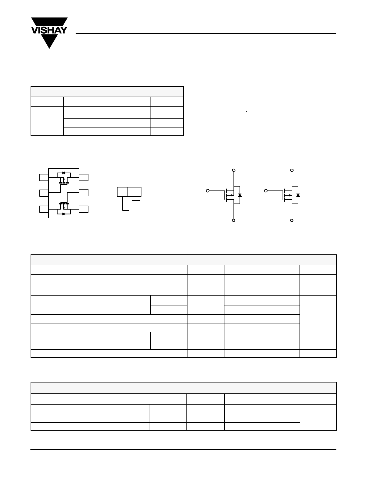
SC-70 (6-LEADS)
1
S
1
2
G
1
3
D
2
SOT-363
0.750 @ VGS = -2.5 V - 0.81
1.10 @ VGS = -1.8 V - 0.67
6
5
4
New Product
Dual P-Channel 20-V (D-S) MOSFET
FEATURES
D TrenchFETr Power MOSFETS: 1.8-V Rated
DS(on)
D
1
G
2
S
2
(W) I
Marking Code
DC XX
YY
Lot Traceability
and Date Code
Part # Code
D
-1.0
(A)
G
D Thermally Enhanced SC-70 Package
APPLICATIONS
D Load Switching
D PA Switch
D Level Switch
S
1
1
Vishay Siliconix
S
2
G
2
D
Top View
1
ABSOLUTE MAXIMUM RATINGS (TA = 25_C UNLESS OTHERWISE NOTED)
Parameter Symbol 5 secs Steady State Unit
Drain-Source Voltage V
Gate-Source Voltage V
a
a
Continuous Drain Current (TJ = 150_C)
Pulsed Drain Current I
Continuous Diode Current (Diode Conduction)
Maximum Power Dissipation
Operating Junction and Storage Temperature Range TJ, T
_
a
a
TA = 25_C
TA = 85_C
TA = 25_C 0.74 0.57
TA = 85_C
P
I
DM
I
DS
GS
D
S
D
stg
- 1.0
- 0.72 -0.63
-0.61 -0.48
0.38 0.30
-20
"8
-3
-55 to 150 _C
THERMAL RESISTANCE RATINGS
Parameter Symbol Typical Maximum Unit
Maximum Junction-to-Ambient
Maximum Junction-to-Foot (Drain) Steady State R
Notes
a. Surface Mounted on 1” x 1” FR4 Board.
a
t v 5 sec 130 170
Steady State
R
thJA
thJF
170 220
80 100
-0.88
D
2
V
A
W
_C/W
Document Number: 71965
S-21482—Rev. A, 26-Aug-02
www.vishay.com
1
Page 2
Si1913DH
W
Vishay Siliconix
New Product
SPECIFICATIONS (TJ = 25_C UNLESS OTHERWISE NOTED)
Parameter Symbol T est Condition Min Typ Max Unit
Static
Gate Threshold Voltage V
Gate-Body Leakage I
Zero Gate Voltage Drain Current I
On-State Drain Current
Drain-Source On-State Resistance
Forward Transconductance
Diode Forward Voltage
Dynamic
b
a
a
a
a
Total Gate Charge Q
Gate-Source Charge Q
Gate-Drain Charge Q
Turn-On Delay Time t
Rise Time t
Turn-Off Delay Time t
Fall Time t
Reverse Recovery Time t
Notes
a. Pulse test; pulse width v 300 ms, duty cycle v 2%.
b. Guaranteed by design, not subject to production testing.
GS(th)
GSS
DSS
I
D(on)
r
DS(on)
DS(on)
g
V
d(on)
d(off)
fs
SD
g
gs
gd
r
f
rr
VDS = VGS, I
= -100 mA -0.45 1 V
D
VDS = 0 V, VGS = "8 V
VDS = -16 V, VGS = 0 V -1
VDS = -16 V, VGS = 0 V, TJ = 85_C -5
VDS = -5 V, VGS = -4.5 V -2 A
VGS = -4.5 V, ID = -0.88 A 0.400 0.490
VGS = -2.5 V, I
VGS = -1.8 V, I
= -0.71 A
D
= -0.2 A
D
VDS = -10 V, ID = -0.88 A 1.5 S
IS = -0.47 A, VGS = 0 V -0.85 -1.2 V
V
= -10 V, VGS = -4.5 V, ID = -0.88 A 0.3 nC
DS
VDD = -10 V, RL = 20 W
VDD = -10 V, RL = 20
ID ^ -0.5 A, V
= -4.5 V, RG = 6 W
GEN
IF = 0.47 A, di/dt = 100 A/ms
"100 nA
0.610 0.750
0.850 1.10
1.2 1.8
0.21
18 30
25 40
15 45
12 20
30 60
mA
W
ns
www.vishay.com
2
Document Number: 71965
S-21482—Rev . A, 26-Aug-02
Page 3
Si1913DH
New Product
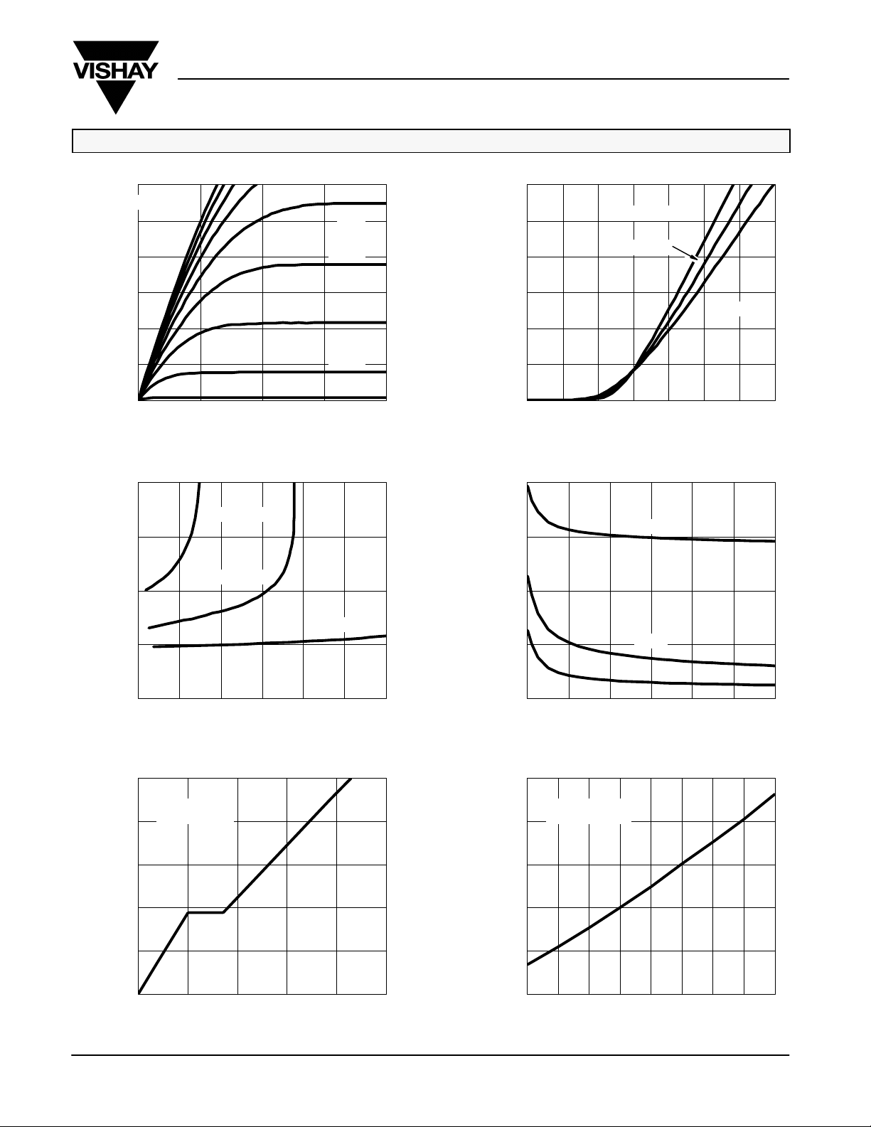
TYPICAL CHARACTERISTICS (25_C UNLESS NOTED)
3.0
VGS = 5 thru 3 .5V
2.5
2.0
1.5
1.0
- Drain Current (A)I
D
0.5
0.0
01234
1.6
Output Characteristics Transfer Characteristics
3 V
2.5 V
2 V
1.5 V
1 V
VDS - Drain-to-Source Voltage (V)
On-Resistance vs. Drain Current
Vishay Siliconix
3.0
2.5
2.0
1.5
1.0
- Drain Current (A)I
D
0.5
0.0
0.0 0.5 1.0 1.5 2.0 2.5 3.0 3.5
VGS - Gate-to-Source Voltage (V)
160
TC = -55_C
25_C
Capacitance
125_C
W )
- On-Resistance (r
DS(on)
- Gate-to-Source Voltage (V)
GS
V
VGS = 1.8 V
1.2
0.8
0.4
0.0
0.0 0.5 1.0 1.5 2.0 2.5 3.0
VGS = 2.5 V
VGS = 4.5 V
ID - Drain Current (A)
Gate Charge
5
VDS = 10 V
I
= 0.9 A
D
4
3
2
1
120
80
C - Capacitance (pF)
40
C
rss
0
024681012
On-Resistance vs. Junction Temperature
1.6
VGS = 4.5 V
I
W)
(Normalized)
- On-Resistance (r
DS(on)
1.4
1.2
1.0
0.8
D
C
iss
C
oss
V
- Drain-to-Source Voltage (V)
DS
= 0.88 A
0
0.0 0.3 0.6 0.9 1.2 1.5
Document Number: 71965
S-21482—Rev . A, 26-Aug-02
Qg - Total Gate Charge (nC)
0.6
-50 -25 0 25 50 75 100 125 150
T
- Junction Temperature (_C)
J
www.vishay.com
3
Page 4

Si1913DH
Vishay Siliconix
New Product
TYPICAL CHARACTERISTICS (25_C UNLESS NOTED)
Source-Drain Diode Forward Voltage On-Resistance vs. Gate-to-Source Voltage
2
1
- Source Current (A)I
S
0.1
0 0.2 0.6 0.8
0.30
0.25
0.20
0.15
0.10
Variance (V)V
0.05
GS(th)
-0.00
-0.05
-0.10
-0.15
-50 -25 0 25 50 75 100 125 150
TJ = 150_C
TJ = 25_C
0.4
VSD - Source-to-Drain Voltage (V) VGS - Gate-to-Source Voltage (V)
1.0 1.2
Threshold Voltage
ID = 100 mA
TJ - Temperature (_C)
1.6
1.2
W )
0.8
- On-Resistance (r
0.4
DS(on)
0.0
Power (W)
ID = 0.88 A
012345
Single Pulse Power, Junction-to-Ambient
5
4
3
2
1
0
1 600100.10.01
Time (sec)
100
www.vishay.com
4
Safe Operating Area, Junction-to-Ambient
10
I
Limited
DM
r
Limited
DS(on)
1
I
D(on)
Limited
- Drain Current (A)I
0.1
D
0.01
TA = 25_C
Single Pulse
BV
Limited
DSS
0.1 1 10 100
VDS - Drain-to-Source Voltage (V)
P(t) = 0.0001
P(t) = 0.001
P(t) = 0.01
P(t) = 0.1
P(t) = 1
P(t) = 10
dc
Document Number: 71965
S-21482—Rev . A, 26-Aug-02
Page 5

Si1913DH
New Product
TYPICAL CHARACTERISTICS (25_C UNLESS NOTED)
Normalized Thermal Transient Impedance, Junction-to-Ambient
2
1
Duty Cycle = 0.5
0.2
0.1
0.1
0.01
0.05
0.02
Single Pulse
-4
10
-3
10
-2
10
-1
Square Wave Pulse Duration (sec)
Normalized Thermal Transient Impedance, Junction-to-Foot
2
Thermal Impedance
Normalized Effective Transient
Vishay Siliconix
Notes:
P
DM
t
1
t
2
t
thJA
t
thJA
100
1
2
= 170_C/W
(t)
1. Duty Cycle, D =
2. Per Unit Base = R
3. TJM - TA = PDMZ
4. Surface Mounted
1 10 60010
1
0.1
Thermal Impedance
Normalized Effective Transient
0.01
10
Duty Cycle = 0.5
0.2
0.1
0.05
Single Pulse
-4
0.02
-3
10
-2
10
-1
11010
Square Wave Pulse Duration (sec)
Document Number: 71965
S-21482—Rev . A, 26-Aug-02
www.vishay.com
5
Page 6

Legal Disclaimer Notice
Vishay
Notice
Specifications of the products displayed herein are subject to change without notice. Vishay Intertechnology, Inc.,
or anyone on its behalf, assumes no responsibility or liability for any errors or inaccuracies.
Information contained herein is intended to provide a product description only. No license, express or implied, by
estoppel or otherwise, to any intellectual property rights is granted by this document. Except as provided in Vishay's
terms and conditions of sale for such products, Vishay assumes no liability whatsoever, and disclaims any express
or implied warranty, relating to sale and/or use of Vishay products including liability or warranties relating to fitness
for a particular purpose, merchantability, or infringement of any patent, copyright, or other intellectual property right.
The products shown herein are not designed for use in medical, life-saving, or life-sustaining applications.
Customers using or selling these products for use in such applications do so at their own risk and agree to fully
indemnify Vishay for any damages resulting from such improper use or sale.
Document Number: 91000 www.vishay.com
Revision: 08-Apr-05 1
Page 7

 Loading...