

Page 1
Dual N-Channel 20-V (D-S) MOSFET
e
A
X
Lot T
Y
Si1902DL
Vishay Siliconix
PRODUCT SUMMARY
VDS (V) r
0.385 at V
20
0.630 at V
(Ω)I
DS(on)
= 4.5 V 0.70
GS
= 2.5 V 0.54
GS
D
(A)
FEATURES
• TrenchFET® Power MOSFETS: 2.5 V Rated
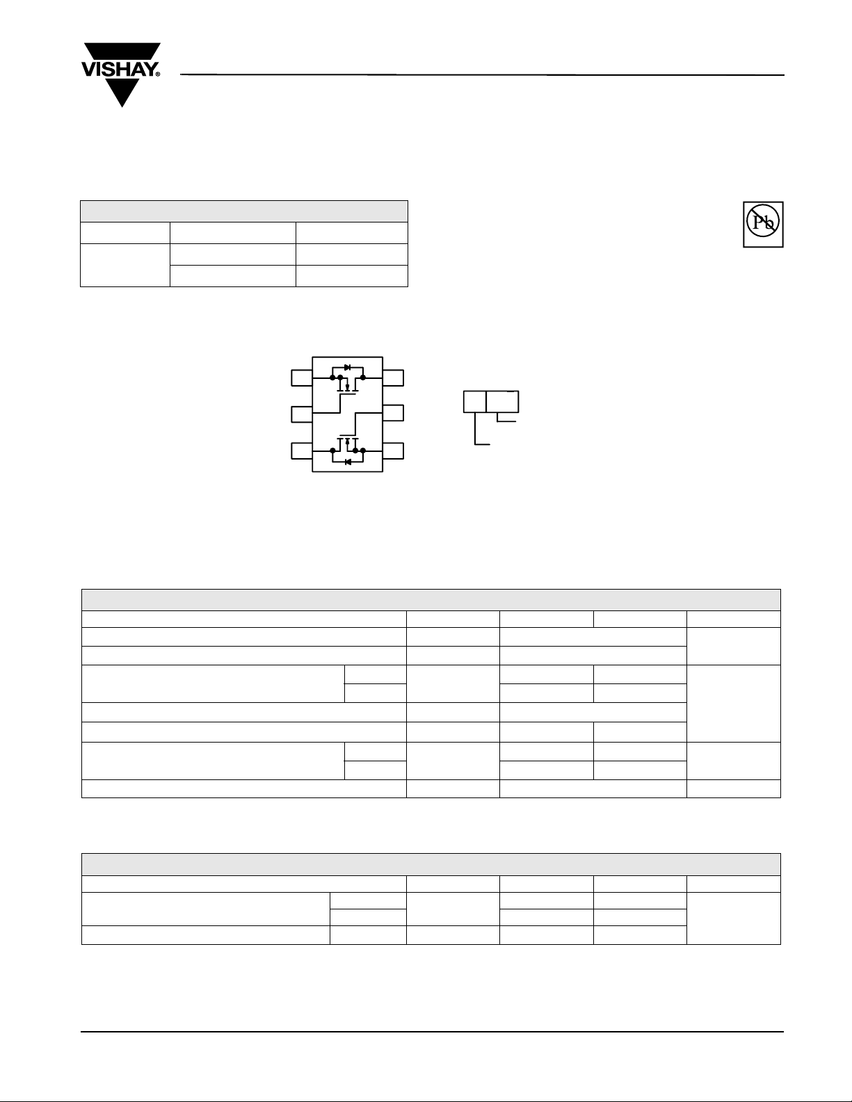
SOT-363
SC-70 (6-LEADS)
S
1
1
G
2
1
D
3
2
Top V
iew
Ordering Information: Si1902DL-T1 (with Tape and Reel)
Si1902DL-T1-E3 (Lead (Pb)-free with Tape and Reel)
D
6
1
5
G
2
S
4
2
M arking Cod
Marking Code
P
X
X
PA
YY
Y
Lot Traceability
and Date Code
Part # Code
ABSOLUTE MAXIMUM RATINGS TA = 25 °C, unless otherwise noted
Parameter Symbol 5 secs Steady State Unit
Drain-Source Voltage V
Gate-Source Voltage V
Continuous Drain Current (T
Pulsed Drain Current
= 150 °C)
J
a
Continuous Source Current (Diode Conduction)
Maximum Power Dissipation
a
TA = 25 °C
= 85 °C 0.50 0.48
T
A
a
T
= 25 °C
A
T
= 85 °C 0.16 0.14
A
Operating Junction and Storage Temperature Range T
DS
GS
I
D
I
DM
I
S
P
D
, T
J
stg
0.70 0.66
0.25 0.23
0.30 0.27
20
±12
1.0
W
- 55 to 150 °C
V
A
Pb-free
Available
RoHS*
COMPLIANT
THERMAL RESISTANCE RATINGS
Parameter Symbol Typical Maximum Unit
Maximum Junction-to-Ambient
a
Maximum Junction-to-Foot (Drain)
t ≤ 5 sec
Steady State 400 460
R
Steady State R
Notes
a. Surface Mounted on 1" x 1" FR4 Board.
* Pb containing terminations are not RoHS compliant, exemptions may apply
Document Number: 71080
S-51415–Rev. H, 03-Apr-06
thJA
thJF
360 415
°C/W
300 350
www.vishay.com
1
Page 2
Si1902DL
Vishay Siliconix
SPECIFICATIONS TJ = 25 °C, unless otherwise noted
Parameter Symbol Test Conditions Min Typ Max Unit
Static
V
Gate Threshold Voltage V
Gate-Body Leakage
Zero Gate Voltage Drain Current
On-State Drain Current
a
Drain-Source On-State Resistance
Forward Transconductance
Diode Forward Voltage
Dynamic
b
a
a
GS(th)
I
GSS
I
DSS
I
V
D(on)
a
r
DS(on)
g
fs
V
SD
Total Gate Charge Qg
Gate-Source Charge Q
Gate-Drain Charge Q
Tur n - O n Del ay T i m e t
Rise Time t
Turn-Off DelayTime t
Fall Time t
Source-Drain Reverse Recovery
Time
gs
gd
d(on)
r
d(off)
f
t
rr
V
DS
0.30
I
10 20
D
Notes:
a. Pulse test; pulse width ≤ 300 µs, duty cycle ≤ 2 %.
b. Guaranteed by design, not subject to production testing.
= VGS, ID = 250 µA 0.6 1.5 V
DS
VDS = 0 V, VGS = ± 12 V ± 100
V
= 16 V, VGS = 0 V 1
DS
V
DS
= 16 V
DS
V
GS
V
GS
V
DS
= 0 V, TJ = 85°C 5
GS
≥ 5 V, V
= 4.5 V 1.0 A
GS
= 4.5 V, ID = 0.66 A 0.320 0.385
= 2.5 V, ID = 0.40 A 0.560 0.630
= 10 V, ID = 0.66 A 1.5 S
IS = 0.23 A, VGS = 0 V 0.8 1.2 V
0.8 1.2
= 10 V, V
= 4.5 V, ID = 0.66 A
GS
0.06
10 20
V
= 10 V, RL = 20 Ω
DD
≅ 0.5 A, V
= 4.5 V, RG = 6 Ω
GEN
16 30
10 20
IF = 0.23 A, di/dt = 100 A/µs 20 40
nA
µA
Ω
nC
ns
Stresses beyond those listed under “Absolute Maximum Ratings” may cause permanent damage to the device. These are stress ratings only, and functional operation
of the device at these or any other conditions beyond those indicated in the operational sections of the specifications is not implied. Exposure to absolute maximum
rating conditions for extended periods may affect device reliability.
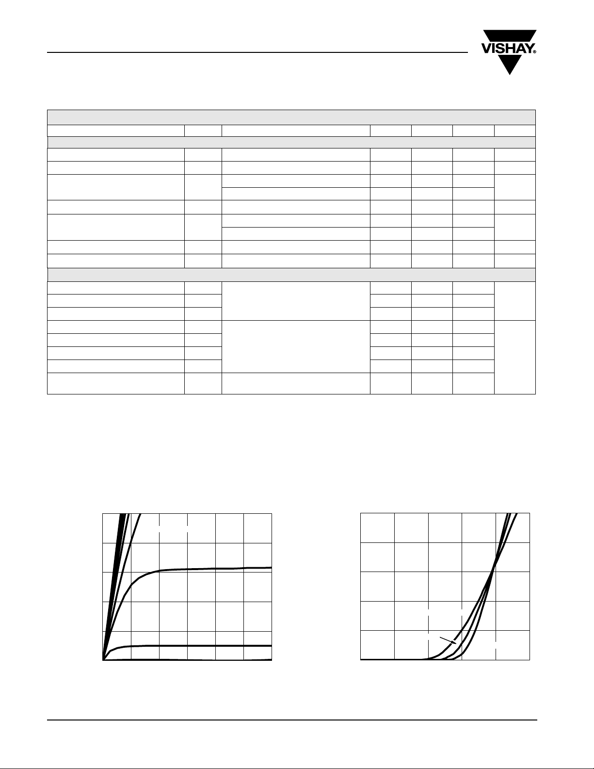
TYPICAL CHARACTERISTICS TA = 25 °C, unless otherwise noted
1.0
VGS = 5 thru 2.5 V
0.8
0.6
0.4
– Drain Current (A)I
D
0.2
0.0
0.0 0.5 1.0 1.5 2.0 2.5 3.0
– Drain-to-Source Voltage (V)
V
DS
1.5 V
Output Characteristics
2 V
1 V
1.0
0.8
0.6
0.4
– Drain Current (A)I
D
0.2
0.0
0.0 0.5 1.0 1.5 2.0 2.5
V
TC = 125 °C
25 °C
– Gate-to-Source Voltage (V)
GS
- 55 °C
Transfer Characteristics
www.vishay.com
2
Document Number: 71080
S-51415–Rev. H, 03-Apr-06
Page 3
1.0
)
Si1902DL
Vishay Siliconix
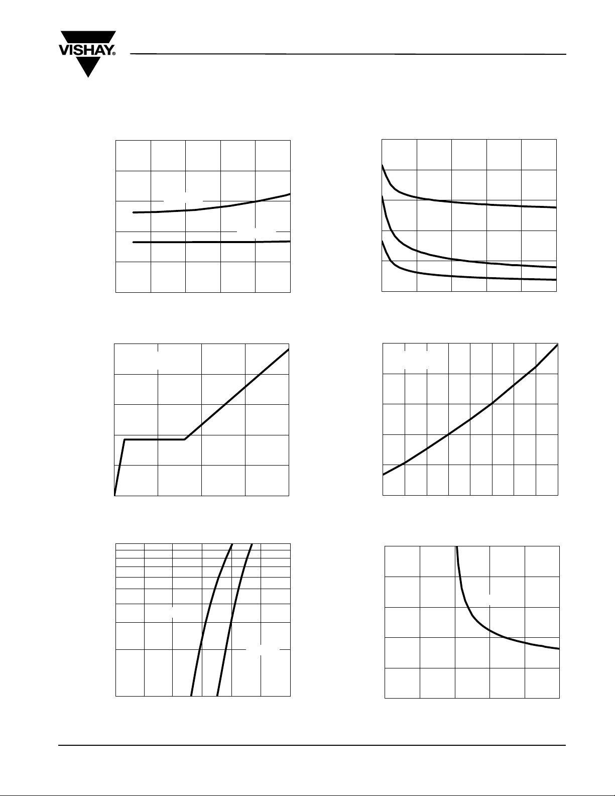
TYPICAL CHARACTERISTICS T
)
0.8
Ω
V
= 2.5 V
0.6
0.4
– On-Resistance (r
DS(on)
0.2
0.0
0.0 0.2 0.4 0.6 0.8 1.0
On-Resistance vs. Drain Current
5
V
= 10 V
DS
= 0.66 A
I
D
4
3
GS
I
– Drain Current (A)
= 25 °C, unless otherwise noted
A
V
= 4.5 V
GS
C – Capacitance (pF)
100
80
C
60
40
C
oss
20
C
rss
0
0 4 8 121620
VDS – Drain-to-Source Voltage (V)
iss
Capacitance
1.6
V
= 4.5 V
GS
= 0.66 A
I
1.4
1.2
D
– Gate-to-Source Voltage (V)
GS
V
– Source Current (A)I
S
2
1
0
0.0 0.2 0.4 0.6 0.8
Qg – Total Gate Charge (nC)
Gate Charge
1
T
= 150 °C
J
T
= 25 °C
J
0.1
0.0 0.2 0.4 0.6 0.8 1.0 1.2
V
– Source-to-Drain Voltage (V
Surge-Drain Diode Forward Voltage
– On-Resistancer
DS(on)
Ω)
– On-Resistance (r
DS(on)
1.0
(Normalized)
0.8
0.6
- 50 - 25
025 50 7
– Junction T emperature (°C)
T
J
5 100 125 150
On-Resistance vs. Junction Temperature
1.0
0.8
I
= 0.66 A
0.6
0.4
0.2
0.0
012345
VGS – Gate-to-Source Voltage (V)
D
On-Resistance vs. Gate-to-Source Voltage
Document Number: 71080
S-51415–Rev. H, 03-Apr-06
www.vishay.com
3
Page 4

Si1902DL
)
Vishay Siliconix
TYPICAL CHARACTERISTICS T
0.2
0.1
= 250 μA
I
D
- 0.0
- 0.1
Variance (V)V
GS(th)
- 0.2
- 0.3
- 0.4
- 50 - 25 025 50 75 100 125 150
2
1
Duty Cycle = 0.5
0.2
0.1
0.1
Thermal Impedance
Normalized Effective Transient
0.05
0.02
0.01
-4
10
T
– Temperature (°C)
J
Threshold Voltage
Single Pulse
-3
10
Normalized Thermal Transient Impedance, Junction-to-Ambient
= 25 °C, unless otherwise noted
A
Power (W)
10
-2
-1
Square Wave Pulse Duration (sec)
5
4
3
2
1
0
-3
10
10
-1
-2
1 100 6001010
Time (sec
Single Pulse Power, Junction-to-Ambient
Notes:
P
DM
t
1
t
2
t
DMZthJA
1
t
2
= 400 °C/W
thJA
(t)
100
1. Duty Cycle, D =
2. Per Unit Base = R
– TA = P
3. T
JM
4. Surface Mounted
1 10 60010
www.vishay.com
4
Document Number: 71080
S-51415–Rev. H, 03-Apr-06
Page 5

TYPICAL CHARACTERISTICS TA = 25 °C, unless otherwise noted
2
1
Duty Cycle = 0.5
0.2
0.1
0.1
Thermal Impedance
Normalized Effective Transient
0.05
0.02
Si1902DL
Vishay Siliconix
0.01
Single Pulse
-4
10
-3
10
-2
10
Square Wave Pulse Duration (sec)
-1
11010
Normalized Thermal Transient Impedance, Junction-to-Foot
Vishay Siliconix maintains worldwide manufacturing capability. Products may be manufactured at one of several qualified locations. Reliability data for Silicon Technology and Package Reliability represent a composite of all qualified locations. For related documents such as package/tape drawings, part marking, and reliability
data, see http://www.vishay.com/ppg?71080.
Document Number: 71080
www.vishay.com
S-51415–Rev. H, 03-Apr-06
5
Page 6

Legal Disclaimer Notice
Vishay
Notice
Specifications of the products displayed herein are subject to change without notice. Vishay Intertechnology, Inc.,
or anyone on its behalf, assumes no responsibility or liability for any errors or inaccuracies.
Information contained herein is intended to provide a product description only. No license, express or implied, by
estoppel or otherwise, to any intellectual property rights is granted by this document. Except as provided in Vishay's
terms and conditions of sale for such products, Vishay assumes no liability whatsoever, and disclaims any express
or implied warranty, relating to sale and/or use of Vishay products including liability or warranties relating to fitness
for a particular purpose, merchantability, or infringement of any patent, copyright, or other intellectual property right.
The products shown herein are not designed for use in medical, life-saving, or life-sustaining applications.
Customers using or selling these products for use in such applications do so at their own risk and agree to fully
indemnify Vishay for any damages resulting from such improper use or sale.
Document Number: 91000 www.vishay.com
Revision: 08-Apr-05 1
Page 7

 Loading...