

Page 1
2
A
LightCharger™ 2.5 Gb/s Automatic Gain Control Amplifier
Applications
SONET/SDH-based transmission systems, test
equipment and modules
OC-48 fibre optic modules
Gigabit Ethernet
Fibre Channel
Wideband RF gain block
Features
Single +3.3 V supply
Power dissipation = 230 mW (typ)
Noise figure < 12 dB
Small signal gain = 23.5 dB differential
Fully integrated AGC function
On-chip 50 Ω input and output terminations
Wide bandwidth (–3 dB) > 2.0 GHz
Maximum input level of 200 mVpk
AGC output level of 370 mVpk differential
Loss of signal functionality
Single-ended or differential operation
Minimal external components
Operating ambient temperature range = -40°C to
+85°C
Equivalent to Nortel Networks AC10
Ordering Information
SE1230Q
Final
Product Description
SiGe Semiconductor offers a portfolio of optical
networking ICs for use in high-performance optical
transmitter and receiver functions, from 155 Mb/s up
to 12.5 Gb/s.
SiGe Semiconductor’s SE1230 is a fully integrated
AGC amplifier aimed primarily at SONET OC-48 and
SDH STM-16 systems. The device may also be used
in any datacom application with input data rates up to
2.5 Gb/s.
The device is designed with differential I/Os and
signal levels compatible with SiGe Semiconductor’s
SE1030 and SE1031 transimpedance amplifiers. A
system block diagram is shown after the functional
description, on page 4.
Optimum performance is provided by differential
connections but with appropriate terminations, the
device can also be used in single-ended mode if
required by the application.
Type Package Remark
SE1230Q 5 mm, 32 pin LQFP None
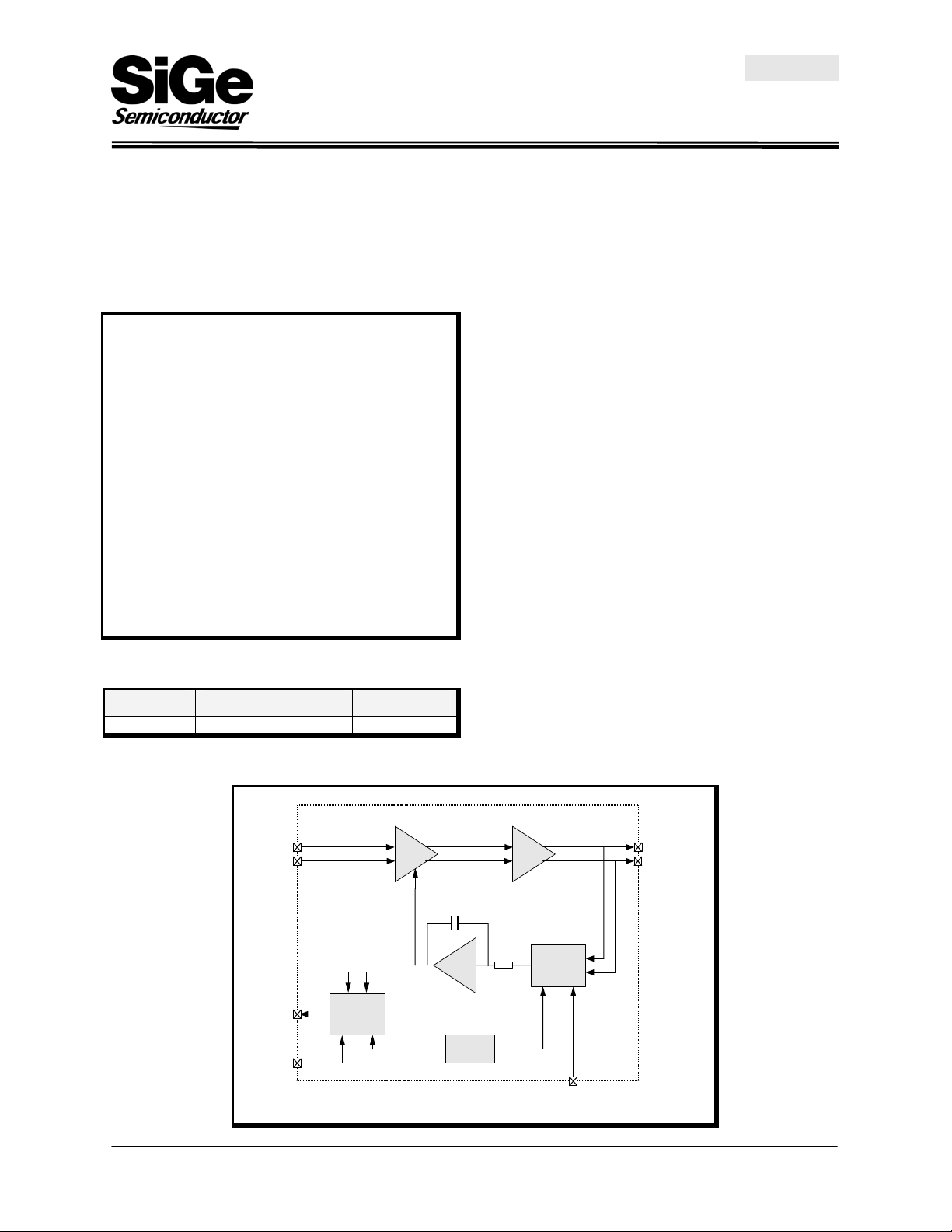
Functional Block Diagram
INP
INN
LOS
LOS_INIT
SE1230
AGC Amp
2.5 Gb/s
Recti fie r/
Comparator
Variable
OUTN OUTP
Gain
Vref
OUTP
Outp ut
Integr ator
Bandgap
Ref
Buffer
Recti fi er
Vref1
GC_ADJ
OUTN
49-DST-01 Rev 1.4 Apr 29/02 1 of 9
Page 2
A
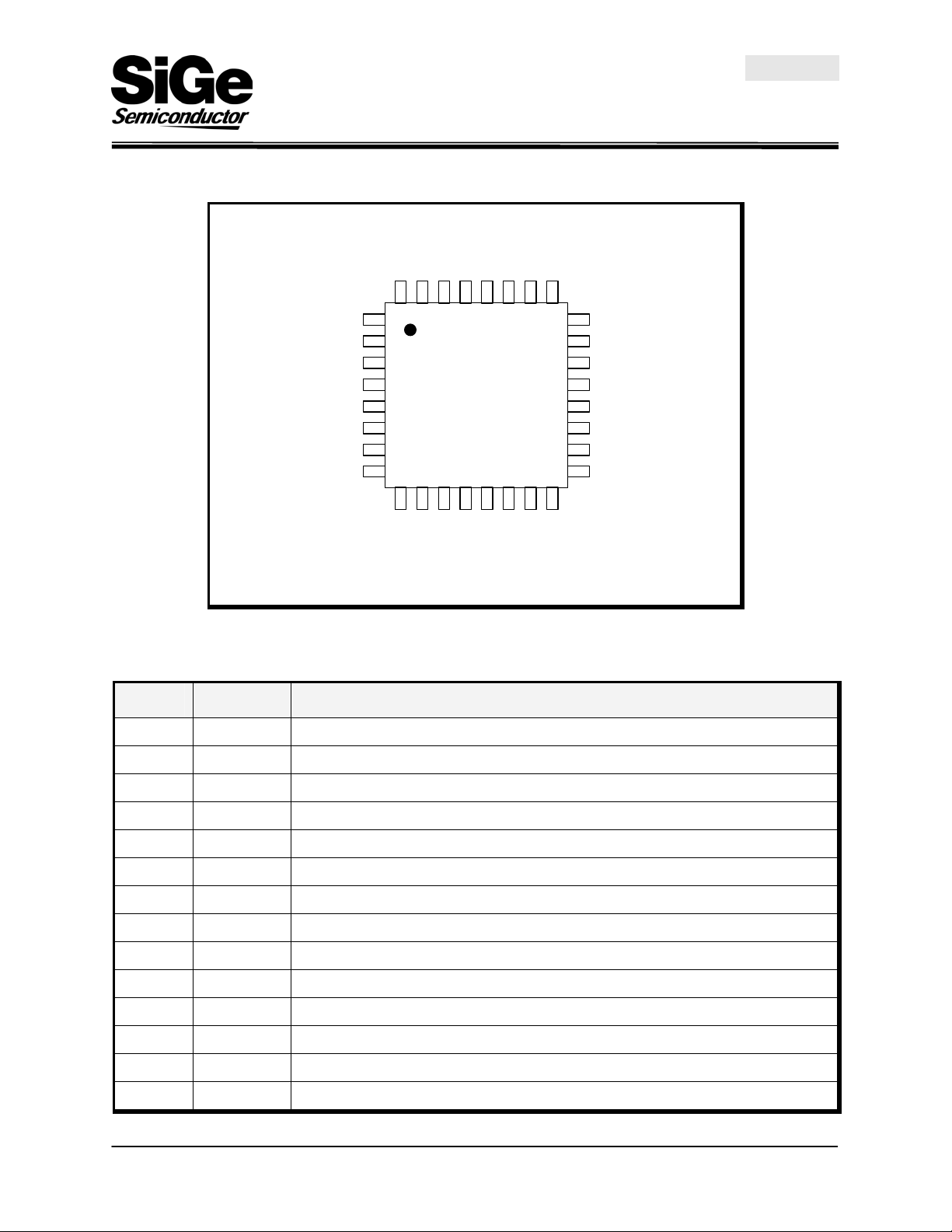
Pin Out Diagram
SE1230Q
LightCharger™ 2.5 Gb/s Automatic Gain Control Amplifier
Final
Pin Out Description
GND
GND
INP
GND
INN
GND
VCC
VCC
VCC
VCC
323130
1
2
3
4
5
6
7
8
9 10 11 12 13 14 15
GND
GND
DNC
DNC DNC
2928272625
Top
View
LOS
VCC
VCC
GC_ADJ
LOS_INIT
VCC VCC
24
23
22
21
20
19
18
17
16
16
GND
GND
GND
GND
OUTP
GND
OUTN
GND
VCC
VCC
Pin No. Name Description
1 GND Negative supply (0 V)
2 GND Negative supply (0 V)
3 INP
4 GND Negative supply (0 V)
5 INN
6 GND Negative supply (0 V)
7 VCC Positive supply (3.3 V)
8 VCC Positive supply (3.3 V)
9 GND Negative supply (0 V)
10 GND Negative supply (0 V)
11 LOS Loss of signal output (open collector)
12 VCC Positive supply (3.3 V)
13 VCC Positive supply (3.3 V)
14 LOS_INIT Sets initial state of LOS output
Non-inverting input (50 Ω impedance)
Inverting input (50 Ω impedance)
49-DST-01 Rev 1.4 Apr 29/02 2 of 9
Page 3
LightCharger™ 2.5 Gb/s Automatic Gain Control Amplifier
Pin No. Name Description
15 GND Negative supply (0 V)
16 GND Negative supply (0 V)
17 VCC Positive supply (3.3 V)
18 VCC Positive supply (3.3 V)
19 GND Negative supply (0 V)
SE1230Q
Final
20 OUTN
21 GND Negative supply (0 V)
22 OUTP
23 GND Negative supply (0 V)
24 GND Negative supply (0 V)
25 VCC Positive supply (3.3 V)
26 VCC Positive supply (3.3 V)
27 AGC_ADJ AGC output level adjust
28 DNC Do not connect
29 DNC Do not connect
30 DNC Do not connect
31 VCC Positive supply (3.3 V)
32 VCC Positive supply (3.3 V)
Inverted output (50 Ω impedance)
Non-inverted output (50 Ω impedance)
49-DST-01 Rev 1.4 Apr 29/02 3 of 9
Page 4

A
LightCharger™ 2.5 Gb/s Automatic Gain Control Amplifier
Functional Description
The SE1230 is configured as a variable gain amplifier,
with automatic gain control. It comprises a variable-
gain block driving a 50 Ω output driver (see the
functional block diagram on page 1). The device
requires a single +3.3 V power supply.
System Inputs
The inputs INP and INN are differential and are each
internally terminated to 50 Ω. To avoid problems with
offset or common-mode voltage, use AC-coupling for
differential or single-ended connection (for the latter,
AC-couple the unused input to ground via 50 Ω). The
maximum input level is 200 mVpk, applied singleended or differentially.
System Outputs
The outputs OUTP and OUTN are differential and are
each internally terminated to 50 Ω. To avoid
problems with offset or common-mode voltage, use
AC-coupling for differential or single-ended
connection (for the latter, AC-couple the unused
output to ground via 50 Ω). The default output level
(under AGC) is 370 mVpk differential.
System Block Diagram
SE1230Q
Final
Automatic Gain Control (AGC)
A rectifier compares the output signal voltage with a
reference level to invoke gain control. When
operating in the controlled gain region, the fully
integrated long time-constant integrator provides
filtered control voltages to the variable gain stages to
maintain a fixed output level. This output level may
be varied by injecting current into AGC_ADJ (leave
unconnected if adjustment is not required).
Loss of Signal
A two-level comparator block is used to detect the
input signal level. If it drops below the lower
threshold, LOS goes low. This output is an open
collector to allow wired-OR connection to other
system alarm signals; it requires an external pull-up
resistor. It goes high only when the input level
exceeds the upper comparator threshold level. If this
function is not required, LOS may be left
unconnected.
By connecting an external series-RC to the LOS_INIT
pin, LOS can be forced low on first power up if the
signal level is between the upper and lower
comparator thresholds. If this function is not required,
leave LOS_INIT unconnected.
Receiver Module
2.5 GHz
2.5 Gb/s
2
2
Clock
Clock & Data
Data
Recovery
2
SE1230Q
GC
2
SE1030/31
TZ
Amplifier
PIN
Amplifier
49-DST-01 Rev 1.4 Apr 29/02 4 of 9
Page 5

SE1230Q
LightCharger™ 2.5 Gb/s Automatic Gain Control Amplifier
Final
Absolute Maximum Ratings
These are stress ratings only. Exposure to stresses beyond these maximum ratings may cause permanent damage
to, or affect the reliability of the device. Avoid operating the device outside the recommended operating conditions
defined below.
Symbol Parameter Min Max Unit
VCC Supply Voltage –0.5 5.0 V
VIO Voltage at any input or output –0.5 VCC+0.5 V
I
IO
IIO Current sourced into pins OUTP and OUTN –40 40 mA
V
ESD
Tstg Storage Temperature –65 150
Recommended Operating Conditions
Symbol Parameter Min Typ Max Unit
Current sourced into any input or output, except
OUTP and OUTN
Electrostatic Discharge (100 pF, 1.5 kΩ), all pins
–20 20 mA
–2 2 kV
°C
VCC Supply Voltage 3.1 3.3 3.5 V
I
LOS Output Load Current 5 mA
LOS
R
LOS_INIT Resistor 1
LOSI
C
LOS_INIT Capacitor (increase value for slow
LOSI
I
AGC_ADJ
Ta Operating Ambient Temperature –40 85
Note 1: This current can be produced by connecting a suitable resistor between VCC and AGC_ADJ.
power supply rise time)
AGC Threshold Adjust Input Current (on
AGC_ADJ pin) – note 1
1
0 150
kΩ
µF
µA
°C
DC Electrical Characteristics
Symbol Parameter Min Typ Max Unit
ICC Supply current 70 100 mA
PD Power Dissipation 230 350 mW
V
V
RT Input/Output Termination Resistance 50
Open-circuit AGC_ADJ Voltage 0.37 V
AGC_ADJ
Output Low Voltage on LOS, with I
LOS
= 1 mA 0.4 V
LOS
Ω
49-DST-01 Rev 1.4 Apr 29/02 5 of 9
Page 6

SE1230Q
LightCharger™ 2.5 Gb/s Automatic Gain Control Amplifier
AC Electrical Characteristics
Symbol Parameter Min Typ Max Unit
BW (3dB) Small Signal Bandwidth at –3dB point 2.0 GHz
Gain
Vin
Small Signal Gain (f = 100 MHz), differential input /
output
21 23.5 26 dB
Maximum Input Signal Level 200
Input Signal Level at AGC Threshold (I
0 µA) – note 2
AGC_ADJ =
25
Lower LOS Threshold (LOS = low) 5 8
Upper LOS Threshold (LOS = high) 12 18
mV pk
(differential)
Final
Output AGC Signal Level (I
V
out
Output AGC Signal Level (I
AGC_ADJ =
AGC_ADJ =
0 µA) – note 3
150 µA) – note
3
250 370 500
80 170 300
(differential)
mV pk
S11 Input Reflection Coefficient (< 1.3 GHz) –10 dB
S22 Output Reflection Coefficient (< 1.3 GHz) –10 dB
NF Noise Figure (diff. in / diff. out) 12 dB
tR / tF
Note 2: Vin at AGC threshold is calculated by dividing V
Note 3: Measured at Vin = 100 mV pk , f = 100 MHz. For intermediate values of I
Output Rise / Fall Time (Input rise / fall time = 20
ps)
by the small signal gain.
out
120 ps
AGC_ADJ
the output
amplitude can be estimated by linear interpolation.
DC and AC electrical characteristics are specified over the recommended operating conditions, and with load resistor
(R
) of 50 Ω, AC coupled via 100 nF, for each output. All characteristics are specified for differential signals on inputs
L
and outputs.
49-DST-01 Rev 1.4 Apr 29/02 6 of 9
Page 7

LightCharger™ 2.5 Gb/s Automatic Gain Control Amplifier
Package Information
The device is packaged in a 5 mm, 32 pin plastic low profile quad flat pack (LQFP).
Package Outline
SE1230Q
Final
Package Dimensions
Dimension Min (mm) Nom (mm) Max (mm)
Lead Count 32
Lead Pitch (E) 0.5
Body Size (D1) 5.00
Component Tip-to-Tip (D) 7.00
Component Height (A) 1.60
Component Standoff 0.05 0.15
Body Thickness (A2) 1.35 1.40 1.45
Lead width (plated) (B) 0.17 0.22 0.27
Lead Thickness (plated) (C) 0.09 0.175
49-DST-01 Rev 1.4 Apr 29/02 7 of 9
Page 8

A
SE1230Q
LightCharger™ 2.5 Gb/s Automatic Gain Control Amplifier
Final
Applications Information
For optimum performance it is recommended that the device be used in differential mode with the circuit shown in the
diagram below. Components connected to LOS, LOS_INIT and AGC_ADJ are optional, depending on whether or not
the loss of signal and/or AGC adjust functions are required.
+3.3 V
TZ Amp,
50 Ω outputs
10 kΩ
LOS
OUTP
OUTN
LOS_INIT
VCC
100 nF
INP
INN
100 nF
GC_ADJ
AGC Amp
SE1230Q
GND
100 nF
100 nF
To system
alarm circuits
CDR,
50 Ω inputs
R
I
AGC_ADJ
0 V
LOSI
1 kΩ
C
LOSI
µ
1
F
49-DST-01 Rev 1.4 Apr 29/02 8 of 9
Page 9

SE1230Q
LightCharger™ 2.5 Gb/s Automatic Gain Control Amplifier
Final
http://www.sige.com
Headquarters: Canada
Phone: +1 613 820 9244
Fax: +1 613 820 4933
2680 Queensview Drive
Ottawa ON K2B 8J9 Canada
sales@sige.com
San Diego United Kingdom
Phone: +1 858 668 3541 South Building, Walden Court
Fax: +1 858 668 3546 Parsonage Lane, Bishop’s Stortford
Hertfordshire CM23 5DB
Hong Kong
Phone: +44 1279 464 200
Phone: +1 852 9177 1917 Fax: +44 1279 464 201
Product Preview
The datasheet contains information from the product concept specification. SiGe Semiconductor Inc. reserves the right to change
information at any time without notification.
Preliminary Information
The datasheet contains information from the design target specification. SiGe Semiconductor Inc. reserves the right to change
information at any time without notification.
Final
The datasheet contains information from the final product specification. SiGe Semiconductor Inc. reserves the right to change
information at any time without notification. Production testing may not include testing of all parameters.
Information furnished is believed to be accurate and reliable and is provided on an “as is” basis. SiGe Semiconductor Inc. assumes
no responsibility or liability for the direct or indirect consequences of use of such information nor for any infringement of patents or
other rights of third parties, which may result from its use. No license or indemnity is granted by implication or otherwise under any
patent or other intellectual property rights of SiGe Semiconductor Inc. or third parties. Specifications mentioned in this publication
are subject to change without notice. This publication supersedes and replaces all information previously supplied. SiGe
Semiconductor Inc. products are NOT authorized for use in implantation or life support applications or systems without express
written approval from SiGe Semiconductor Inc.
RangerCharger
Copyright 2002 SiGe Semiconductor
All Rights Reserved
TM
, StreamChargerTM, PointChargerTM, and LightChargerTM are trademarks owned by SiGe Semiconductor Inc.
49-DST-01 Rev 1.4 Apr 29/02 9 of 9
 Loading...