

Page 1
50 Ω 50 Ω 50 Ω
R
LightChargerTM155 Mb/s Transimpedance Amplifier
Applications
§ SONET/SDH-based transmission systems, test
equipment and modules
§ OC-3 fibre optic modules and line termination
§ ATM and FDDI optical receivers
Features
§ Single +5 V power supply
§ Input noise current = 12 nA rms when used with a
0.5 pF detector
§ Transimpedance gain = 15 kΩ into a 50 Ω load
(single-ended)
§ On-chip automatic gain control gives input
current overload of 2.6 mA pk and max output
voltage swing of 300 mV pk-pk
§ 50 Ω single-ended or 100 Ω differential wire bond
selectable outputs
§ Bandwidth (-3 dB) = 150 MHz (min)
§ Wide data rate range = 10 Mb/s to 155 Mb/s
§ High input bias level = 2 V
§ Minimal external components, supply decoupling
only
§ Operating junction temperature range = -40°C to
+95°C
§ Equivalent to Nortel Networks AB52
Ordering Information
SE1000W
Final
Product Description
SiGe Semiconductor offers a portfolio of optical
networking ICs for use in high-performance optical
transmitter and receiver functions, from 155 Mb/s up
to 12.5 Gb/s.
SiGe Semiconductor’s SE1000W is a fully integrated,
silicon bipolar transimpedance amplifier; providing
wideband, low noise preamplification of signal current
from a photodetector. It features single-ended or
differential outputs, selectable by wire bond options,
and incorporates an automatic gain control
mechanism to increase dynamic range, allowing input
signals up to 2.6 mA peak. For differential outputs, a
decoupling capacitor on the supply is the only
external circuitry required.
Noise performance is optimized for 155 Mb/s
operation, with a calculated rms noise based
sensitivity of –41 dBm for 10
using a detector with 0.5 pF capacitance and a
responsivity of 0.95 A/W, with an infinite extinction
ratio source.
-10
bit error rate, achieved
Type Package Remark
SE1000W Bare Die Shipped in
Waffle Pack
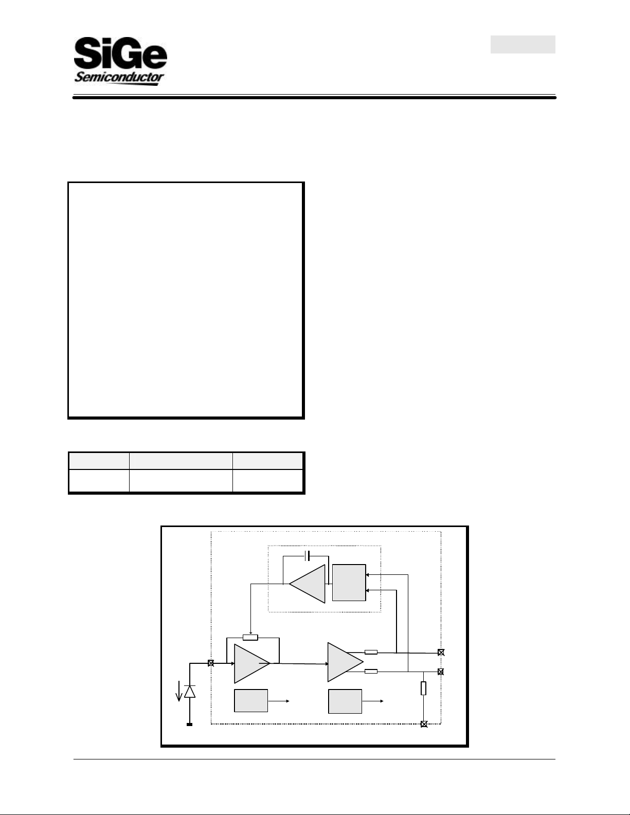
Functional Block Diagram
Input
Current
GND or –ve supply
TZ_IN
SE1000
TzAmp
155 Mb/s
Bandgap
Reference
f
Tz Amp
Automatic Gain Control
Integrator Rectifier
Output
Driver
Power
Supply
Rejection
Wire bond option for single -ended operation
OUTP
OUTN
ACGND
40-DST-01 § Rev 1.5 § May 24/02 1 of 9
Page 2
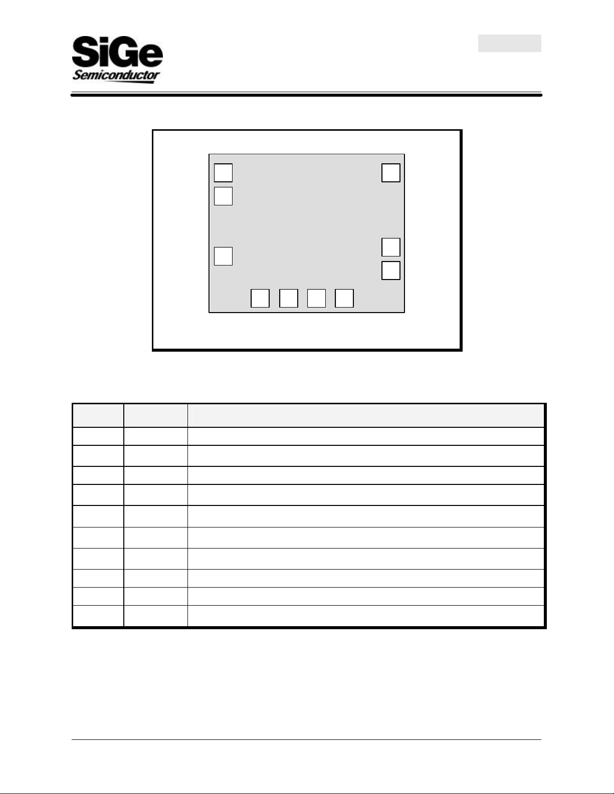
Bondpad Diagram
SE1000W
LightChargerTM155 Mb/s Transimpedance Amplifier
Final
VCC2
VCC1
TZ_IN
1
2
Top
View
3
7 6 5 4
VEE2 VEE1 VEE1 ACGND
10
VCC1
9
OUTP
8
OUTN
Bondpad Description
Pad No. Name Description
1 VCC2 Positive supply (+5.0 V), front end circuitry only.
2 VCC1
3 TZ_IN Input pad (connect to photodetector cathode).
4 VEE2
5 ACGND
6 VEE1
7 VEE1
8 OUTN Negative differential voltage output; leave unconnected for single-ended operation.
Positive supply (+5.0 V), pads 2 & 10 are connected on chip. Only one pad needs to
be bonded.
Negative supply (0V) – Note this is separate ground for the input stage, which is AC
coupled on chip. There is no DC current through this pad.
Bond option: Connected to external capacitor to ground for single-ended operation
(recommended 1 nF); unconnected for differential operation.
Negative supply (0V), pads 6 & 7are connected on chip. Only one pad needs to be
bonded.
Negative supply (0V), pads 6 & 7 are connected on chip. Only one pad needs to be
bonded.
9 OUTP Positive differential or single-ended voltage output.
10 VCC1
Positive supply (+5.0 V), pads 2 & 10 are connected on chip. Only one pad needs to
be bonded.
40-DST-01 § Rev 1.5 § May 24/02 2 of 9
Page 3

LightChargerTM155 Mb/s Transimpedance Amplifier
Functional Description
Amplifier Front-End
The transimpedance front-end amplifies an input
current from a photodetector, at pin TZ_IN, to produce
an output voltage with the feedback resistor Rf
determining the level of amplification (see the
functional block diagram on page 1). An automatic
gain control loop varies this resistor, to ensure that
the output from the front-end does not saturate the
output driver stage that follows. This gain control
allows input signals of up to 2.6 mA peak.
The input pin TZ_IN is biased at 3 V below the supply
voltage VCC, allowing a photodetector to easily be
reverse biased by connecting the anode to ground,
and hence enabling single rail operation.
The front-end stage has its own supply pins, VCC2
(+5 V) and VEE2 (0 V), to achieve optimum noise
performance and maintain integrity of the high-speed
signal path. The remainder of the circuitry uses the
supply pins VCC1 (+5 V) and VEE1 (0 V).
Output driver stage
The output driver acts as a buffer stage, capable of
swinging up to 150 mVpk-pk into a 50 Ω load (or
300 mVpk-pk differential into a 100 Ω load). The
small output swings allow ease of use with low
voltage post amplifiers (e.g. 3.3 V parts).
The output can be configured in a differential or
single-ended mode. For differential operation, the pad
ACGND is not wire bonded and the circuit provides a
fully balanced 100 Ω output, on the pins OUTP and
OUTN. For single-ended operation, the ACGND pad
is required to be wire bonded to an external capacitor
SE1000W
Final
to ground (recommend 1 nF). Under these
circumstances, OUTP operates as a single-ended
50 Ω output. In both cases, increasing optical input
level gives a positive-going output signal on the
OUTP pin.
Automatic Gain Control (AGC)
The AGC circuit monitors the voltages from the output
driver and compares them to an internal reference
level produced via the on-chip bandgap reference
circuit. When this level is exceeded, the gain of the
front-end is reduced by controlling the feedback
resistor Rf.
A long time-constant integrator is used within the
control loop of the AGC with a typical low frequency
cut-off of 5 kHz.
Power Supply Rejection
An on-chip power supply rejection circuit is used to
achieve both single-ended and differential rejection
from the +5 V VCC rail.
This stable DC reference minimizes the variation in
the noise and bandwidth performance of the circuit
due to power supply variation of +4.7 V to +5.3 V.
The AC rejection ensures that performance is not
degraded by noise on the power supply. The circuit
achieves a power supply rejection on the outputs of
40 dB for both single-ended and differential operation,
up to 100 kHz. The use of external decoupling will
help to remove any unwanted signals at higher
frequencies.
40-DST-01 § Rev 1.5 § May 24/02 3 of 9
Page 4

SE1000W
LightChargerTM155 Mb/s Transimpedance Amplifier
Final
Absolute Maximum Ratings
These are stress ratings only. Exposure to stresses beyond these maximum ratings may cause permanent damage
to, or affect the reliability of the device. Avoid operating the device outside the recommended operating conditions
defined below.
Symbol Parameter Min Max Unit
VCC Supply Voltage –0.7 6.0 V
VIO Voltage at any input or output –0.5 VCC+0.5 V
I
IO
IIO Current sourced into pin TZ_IN –5 5 mA
Current sourced into any input or output except
TZ_IN
–20 20 mA
V
ESD
V
ESD
Tstg Storage Temperature –65 150
Electrostatic Discharge (100 pF, 1.5 kΩ) except
TZ_IN
Electrostatic Discharge (100 pF, 1.5 kΩ) pin
TZ_IN
–2 2 kV
–0.25 0.25 kV
Recommended Operating Conditions
Symbol Parameter Min Typ Max Unit
VCC Supply Voltage 4.7 5.0 5.3 V
Tj Operating Junction Temperature –40 95
DC Electrical Characteristics
Symbol Parameter Min Typ Max Unit
ICC Supply Current 39 58 mA
lagc AGC Threshold 4
Vin Input Bias Voltage VCC–3.2 VCC–3.0 VCC–2.7 V
Vout Output Bias Voltage 2.9 3.5 V
µA pk-pk
°C
°C
Rout Output Resistance 35 50 65
Ω
40-DST-01 § Rev 1.5 § May 24/02 4 of 9
Page 5

SE1000W
LightChargerTM155 Mb/s Transimpedance Amplifier
AC Electrical Characteristics
Symbol Parameter Min Typ Max Unit
BW (3dB) Small Signal Bandwidth at –3dB point 150 MHz
Final
Tz
Dri Input Data Rate 10 155 Mb/s
Voutmax Maximum Differential Output Voltage 300 mV pk-pk
Flf Low Frequency Cut -off 5 kHz
PSRR
lOL
Pol Optical Overload +1.4 dBm
Nrms Input Noise Current (in 100 MHz) 12 15 nA rms
DC and AC electrical characteristics are specified under the following conditions:
Supply Voltage (VCC).........................................4.7 V to 5.3 V
Junction Temperature (Tj) ..................................–40°C to 95°C
Load Resistor (RL)...............................................50 Ω AC coupled via 220 nF (single-ended)
Photodetector Capacitance (Cd) .......................0.5 pF
Input bond wire inductance................................1 nH
Photodetector responsivity.................................0.95 A/W
Transimpedance (Tz) measured with 1 µA mean photocurrent
Single-ended Tra nsimpedance (50 Ω on output,
f = 50 MHz)
Power Supply Rejection Ratio (single-ended or
differential) up to 100 kHz
Input Current before overload (155 Mb/s NRZ
data)
11 15 20 kΩ
40 dB
2600
µA pk-pk
40-DST-01 § Rev 1.5 § May 24/02 5 of 9
Page 6

SE1000W
LightChargerTM155 Mb/s Transimpedance Amplifier
Bondpad Configuration
The bondpad center coordinates are referenced to the center of the lower left pad (pad 4). All dimensions are in
microns (µm).
Final
Pad No. Name
1 VCC2 -307.3 679.0
2 VCC1 -307.3 549.0
3 TZ_IN -307.3 315.0
4 VEE2 0 0
5 ACGND 130.0 0
6 VEE1 260.0 0
7 VEE1 390.0 0
8 OUTN 690.7 155.0
9 OUTP 690.7 285.0
10 VCC1 690.7 679.0
X
Coordinate
(µm)
Y
Coordinate
(µm)
40-DST-01 § Rev 1.5 § May 24/02 6 of 9
Page 7

SE1000W
LightChargerTM155 Mb/s Transimpedance Amplifier
Final
The diagram below shows the bondpad configuration of the SE1000W Transimpedance Amplifier. Note that the
diagram is not to scale. All bondpads are 92 µm x 92 µm with a passivation opening of 82 µm x 82 µm. There are two
VCC1 and two VEE1 pads for ease of wire bonding; these pad pairs are connected on-chip and only one pad of each
type is required to be bonded out.
Mechanical die visual inspection criteria per MIL-STD-883 Method 2010.10 Condition B Class Level B.
998.0
998.0
998.0
998.0
130.0
130.0
130.0
130.0
394.0
394.0
394.0
394.0
234.0315.0
234.0315.0
234.0315.0
925.0
925.0
925.0
925.0
234.0315.0
Top
Top
View
View
126.0
126.0
126.0
126.0
130.0 130.0 130.0
130.0 130.0 130.0
130.0 130.0 130.0
130.0 130.0 130.0
307.3
307.3
307.3
307.3
123.0
123.0
123.0
123.0
1250.0
1250.0
1250.0
1250.0
Side View
Side View
All Dimensions in Microns ( µm)
All Dimensions in Microns ( µm)
All Dimensions in Microns ( µm)
All Dimensions in Microns ( µm)
130.0
130.0
130.0
130.0
155.0
155.0
300.7
300.7
400.0
400.0
400.0
400.0
40-DST-01 § Rev 1.5 § May 24/02 7 of 9
Page 8

1 2 10 3 4 6 7 9 8
NC
5
–
ve bias
1 2 10 3 4 6 7 9 8
NC
5
–
ve bias
SE1000W
LightChargerTM155 Mb/s Transimpedance Amplifier
Final
Applications Information
For optimum performance it is recommended that the device be used in differential mod e with the circuit shown in the
first diagram below.
Note that the two VCC1 pads (2, 10) are connected on-chip, as are the VEE1 pads (6, 7), and only one pad of each
type is required to be bonded out. However, in order to minimize inductance for optimum high speed performance, it
is recommended that all power pads are wire bonded. The VEE2 and VCC2 pads are not connected on chip to VEE1
and VCC1 respectively, and must be bonded out separately.
Connections for differential operation:
+5 V
1 nF min
TZ_IN
PIN
0 V or
Connections for single-ended operation:
+5 V
PIN
0 V
TZ_IN
VCC2
TZ Amplifier
VEE2
VCC2
TZ Amplifier
SE1000W
VEE2
VCC1
SE1000W
VEE1
VCC1
VEE1
OUTP
OUTN
ACGND
OUTP
OUTN
ACGND
To 50 O loads,
AC coupled
1 nF min
To 50 O load,
AC coupled
1 nF
0 V or
0 V
40-DST-01 § Rev 1.5 § May 24/02 8 of 9
Page 9

SE1000W
LightChargerTM155 Mb/s Transimpedance Amplifier
Final
http://www.sige.com
Headquarters: Canada
Phone: +1 613 820 9244
Fax: +1 613 820 4933
2680 Queensview Drive
Ottawa ON K2B 8J9 Canada
sales@sige.com
U.S.A. United Kingdom
1150 North First Street 1010 Cambourne Business Park
San Jose, CA Cambourne
USA 95112 Cambridge CB3 6DP
Phone: +1 408 998 5060 Phone: +44 1223 598 444
Fax: +1 408 998 5062 Fax: +44 1223 598 035
Product Preview
The datasheet contains information from the product concept specification. SiGe Semiconductor reserves the right to change
information at any time without notification.
Preliminary
The datasheet contains information from the design target specification. SiGe Semiconductor reserves the right to change
information at any time without notification.
Final
The datasheet contains information from the final product specification. SiGe Semiconductor reserves the right to change
information at any time without notification. Production testing may not include testing of all parameters.
Information furnished is believed to be accurate and reliable and is provided on an “as is” basis. SiGe Semiconductor Inc. assumes
no responsibility or liability for the direct or indirect consequences of use of such information nor for any infringement of patents or
other rights of third parties, which may result from its use. No license or indemnity is granted by implication or otherwise under any
patent or other intellectual property rights of SiGe Semiconductor Inc. or third parties. Specifications mentioned in this publication
are subject to change without notice. This publication supersedes and replaces all information previously supplied. SiGe
Semiconductor Inc. products are NOT authorized for use in implantation or life support applications or systems without express
written approval from SiGe Semiconductor Inc.
LightCharger™ is a trademark owned by SiGe Semiconductor.
Copyright 2002 SiGe Semiconductor
All Rights Reserved
40-DST-01 § Rev 1.5 § May 24/02 9 of 9
 Loading...