

Page 1
S DU/D40N03L
S amHop Microelec tronics C orp.
Augus t , 2002
N-C hannel Logic Level E nhancement Mode Field E ffect T ransis tor
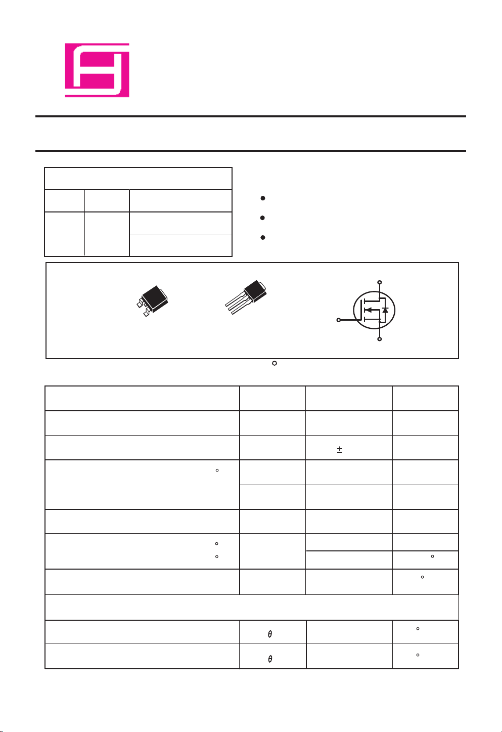
PR ODUC T S UMMAR Y
VDS S
30V
ID
40A
R DS (O N) ( m
9 @ VGS = 10V
13 @ V GS = 4. 5V
D
G
S
S DU S E R IE S
TO-252AA(D-P AK )
W
) TYP
G
D
S
S DD SE RIE S
TO-251(l-P AK)
ABS OLUT E MAXIMUM R ATINGS (TC=25 C unless otherwise noted)
F E ATUR ES
S uper high dense cell design for low R
R ugged and reliable.
TO-252 and T O -251 P ackage.
D
G
S
DS (O N
).
P a rameter
Drain-S ource Voltage
G ate-S ource Voltage 20
Drain C urrent-C ontinuous @ T J =125 C
-P ulsed
a
Drain-S ource Diode F orward C urrent 40
Maximum P ower Dissipation
@ T c=25 C
S ymbol
V
DS
V
G S
I
D
I
DM
I
S
P
D
120
Derate above 25 C
Opera ting and S torage
Temperature R ange
TJ, T
S TG
-55 to 175
THE R MAL C HAR AC TE R IS TIC S
Thermal R esistance, J unction-to-C as e
Thermal R esistance, J unction-to-Ambient
R
R
J C
J A
Limit Unit
30
V
V
40
A
A
A
50
0.3
3
50
W
W / C
C
C
C
/W
/W
1
Page 2
S DU/D40N03L
E LE C T R IC AL C HAR AC TE R IS T IC S (T C =25 C unles s otherwis e noted)
P arameter
OF F C HAR AC TE R IS TIC S
Drain-S ource B reakdown Voltage
S ymbol
B V
DS S
C ondition
V
G S
= 0V, ID = 250uA
Min
30
Typ
Max
Unit
V
Zero G ate Voltage Drain C urrent
G ate-B ody Leakage
ON C HAR AC T E R IS TIC S
a
G ate T hreshold Voltage
Drain-S ource On-S tate R esistance
On-S tate Drain C urrent
DYNAMIC C HAR AC TE R IS TIC S
b
Input C apacitance
Output C apacitance
R evers e T rans fer Capacitance
S WIT C HING C HAR AC T E R IS TIC S
b
I
I
V
G S (th)
R
DS (ON)
I
D(ON)
g
C
C
C
DS S
G S S
F S
IS S
OS S
R S S
V
DS
= 24V, V
V
G S
= 20V, V
V
DS
= V
G S
, ID = 250uA
V
G S
= 10V, ID =20A
V
G S
= 4.5V, ID = 10A
V
DS
= 10V, V
V
DS
= 10V, ID = 20A
V
DD
=15V, V
f = 1.0MH
Z
GS
G S
G S
= 0V
DS
= 0V
= 10V
= 0V
1 1.5
40
9
13
30
1375
670
200
10
100
3
10
16
uA
nA
V
m ohm
m ohm
A
SF orward Trans conductance
P
F
P
F
P
F
Turn-O n Delay Time
R ise Time
Turn-O ff Delay Time
F a ll time
Total G ate C harge
G ate-S ource C harge
G ate-Drain C harge
t
D(ON)
t
t
D(OFF)
t
Q
Q
Q
VDD = 15V,
r
ID =1A,
V
R
f
VDS = 10V,ID = 40A,V
g
VDS = 10V,ID = 40A,V
gs
gd
VDS = 10V, ID = 40A,
V
2
G S
G E N
G S
= 10V,
= 6
=10V
ohm
G S
=10V
G S
=4.5V
30
32
132
30
40
19.5
8.2
5.3
50
23.5
ns
ns
ns
ns
nC
nC
nC
nC
Page 3

S DU/D40N03L
E LE C T R IC AL C HAR AC T E R IS T IC S (TC=25 C unles s otherwis e noted)
P a ra meter
S ymbol
C ondition
Min
Typ
Max
Unit
DR AIN-S OUR C E DIO DE C HAR AC T E R IS T IC S
Diode F orward V oltage
Notes
a.P ulse Test:P ulse W idth 300us , Duty C ycle 2% .
b.Guaranteed by des ign, not s ubject to production tes ting.
40
35
30
25
20
15
10
ID, Dra in C urrent ( A)
5
0
0 0. 5 1 1.5 2 2. 5 3
VDS , Dra in-to-S ource Voltage (V )
F igure 1. Output C haracteris tics F igure 2. Transfer C hara cteris tics
VGS =10, 9,8, 7,6 ,5V
V
S D
VGS =4V
a
V
G S
= 0V, Is = 25A
40
30
20
10
ID, Dra in C urrent ( A)
0
25 C
T j=125 C
-55 C
0 1 2 3 4 5 6
VGS , G ate-to-S ource Voltage (V)
1.3
V
6
360 0
300 0
240 0
180 0
120 0
C , C apa citanc e (pF )
600
0
0 5 1 0 15 20 25 30
VDS , Dra in-to S ource Voltage (V)
F igure 3. Capacitance
C iss
C oss
C rss
1. 3
VGS =10V
1. 2
1. 1
1. 0
0. 9
0. 8
Dra in-S ource, On-R esistanc e
R DS (O N), Normalize d
0. 7
0 10 2 0 30 4 0
ID, Dra in C urrent(A)
T j=125 C
25 C
-55 C
F igure 4. On-R esistance Variation with
Drain C urrent a nd Tempera ture
3
Page 4

S DU/D40N03L
1.15
VDS=V
1.10
1.05
1.00
0.95
Vth, N ormaliz ed
0.90
0.85
6
G ate-S ource T hreshold V oltage
0.80
-50 -25 0 25 50 75 100 125 150
Tj, Junction T emperature ( C)
G S
ID=250uA
F igure 5. G ate Threshold V ariation
with T emperature
60
VDS=10V
50
40
30
20
1.15
1.10
1.05
1.00
0.95
B VDS S , N ormalized
0.90
Dra in-S ource B rea kdown V oltage
0.85
-50 -25 0 25 50 75 100 125 150
Tj, Junction T emperature ( C)
ID=250uA
F igure 6. Brea kdown Voltage V ariation
with T emperature
40
10
1.0
10
gFS , T ransconductance (S )
0
0 5 10 15 20
IDS , Drain-S ource C urrent (A)
F igure 7. Transconductance Variation
with Drain C urrent
10
VDS=10V
8
ID=40A
6
4
2
VGS , G ate to S ource V oltage (V )
0
0 5 10 15 20 2 5 30 35 40
Qg, Total G ate Cha rge (nC )
F igure 9. G ate C harge
4
Is , S ource-drain current (A)
0.1
0.4 0. 6 0.8 1.0 1. 2 1.4
VS D, Body Diode Forward V oltage (V)
F igure 8. Body Diode F orward Voltage
Variation with S ource C urrent
300
200
100
imit
(O N) L
DS
R
10
V
G S
ID, Dra in C urrent (A)
0.5
S ingle P ulse
1
0.1
=10V
Tc=25 C
1 10 30 60
VDS , Drain-S ource Voltage (V)
1ms
10ms
100 ms
1s
DC
F igure 10. Ma ximum S afe
O pera ting Area
Page 5

S DU/D40N03L
DD
V
on
t
d(off)
t
r
d(on)
R
IN
V
V
G S
G EN
R
G
L
D
OU T
V
S
t
OU T
V
IN
V
10%
t
90%
10% 10%
INVE R T E D
50% 50%
P ULS E W IDT H
90%
t
off
f
t
90%
6
F igure 11. S witching Tes t C ircuit
2
1
D=0. 5
0. 2
0. 1
0. 1
0. 05
0. 02
0. 01
-5
10
0. 01
S ING LE P UL S E
-4
10
r(t), Norma lized E ffective
T rans ient Thermal Impedance
F igure 13. Normalized T hermal Transient Impedance C urve
F igure 12. S witching Waveforms
-3
10
S quare W ave P ulse D uration (sec)
-2
10
DM
P
1
t
2
t
1. R θJA (t)=r (t) * R θJA
2. R θJA=S ee Data shee t
3. TJ M-T A = PDM* R θJA ( t)
4. Duty C ycle , D=t1/t2
-1
10
1 10
5
 Loading...